 | –≠–ª–µ–∫—Ç—Ä–æ–Ω–Ω—ã–π –∫–æ–º–ø–æ–Ω–µ–Ω—Ç: LM628 | –°–∫–∞—á–∞—Ç—å:  PDF PDF  ZIP ZIP |

LM628/LM629
Precision Motion Controller
General Description
The LM628/LM629 are dedicated motion-control processors
designed for use with a variety of DC and brushless DC
servo motors, and other servomechanisms which provide a
quadrature incremental position feedback signal. The parts
perform the intensive, real-time computational tasks required
for high performance digital motion control. The host control
software interface is facilitated by a high-level command set.
The LM628 has an 8-bit output which can drive either an
8-bit or a 12-bit DAC. The components required to build a
servo system are reduced to the DC motor/actuator, an in-
cremental encoder, a DAC, a power amplifier, and the
LM628. An LM629-based system is similar, except that it
provides an 8-bit PWM output for directly driving H-switches.
The parts are fabricated in NMOS and packaged in a 28-pin
dual in-line package or a 24-pin surface mount package
(LM629 only). Both 6 MHz and 8 MHz maximum frequency
versions are available with the suffixes -6 and -8, respec-
tively, used to designate the versions. They incorporate an
SDA core processor and cells designed by SDA.
Features
n
32-bit position, velocity, and acceleration registers
n
Programmable digital PID filter with 16-bit coefficients
n
Programmable derivative sampling interval
n
8- or 12-bit DAC output data (LM628)
n
8-bit sign-magnitude PWM output data (LM629)
n
Internal trapezoidal velocity profile generator
n
Velocity, target position, and filter parameters may be
changed during motion
n
Position and velocity modes of operation
n
Real-time programmable host interrupts
n
8-bit parallel asynchronous host interface
n
Quadrature incremental encoder interface with index
pulse input
n
Available in a 28-pin dual in-line package or a 24-pin
surface mount package (LM629 only)
TRI-STATE
Æ
is a registered trademark of National Semiconductor Corporation.
DS009219-1
FIGURE 1. Block Diagram
November 1999
LM628/LM629
Precision
Motion
Controller
© 1999 National Semiconductor Corporation
DS009219
www.national.com
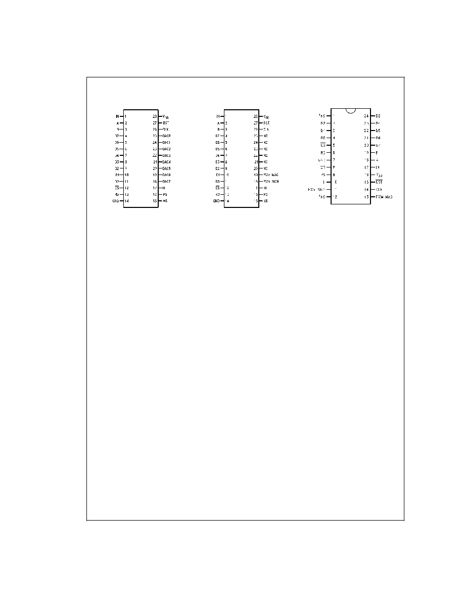
Connection Diagrams
LM628N
DS009219-2
LM629N
DS009219-3
LM629M
DS009219-21
*Do not connect.
Order Number LM629M-6, LM629M-8, LM628N-6, LM628N-8, LM629N-6 or LM629N-8
See NS Package Number M24B or N28B
LM628/LM629
www.national.com
2
Absolute Maximum Ratings
(Note 1)
If Military/Aerospace specified devices are required,
please contact the National Semiconductor Sales Office/
Distributors for availability and specifications.
Voltage at Any Pin with
Respect to GND
-0.3V to +7.0V
Ambient Storage Temperature
-65∞C to +150∞C
Lead Temperature
28-pin Dual In-Line
Package (Soldering, 4 sec.)
260∞C
24-pin Surface Mount
Package (Soldering, 10 sec.)
300∞C
Maximum Power Dissipation
(T
A
85∞C, (Note 2)
605 mW
ESD Tolerance
(C
ZAP
= 120 pF, R
ZAP
= 1.5k)
2000V
Operating Ratings
Temperature Range
-40∞C
<
T
A
<
+85∞C
Clock Frequency:
LM628N-6, LM629N-6,
LM629M-6
1.0 MHz
<
f
CLK
<
6.0 MHz
LM628N-8, LM629N-8,
LM629M-8
1.0 MHz
<
f
CLK
<
8.0 MHz
V
DD
Range
4.5V
<
V
DD
<
5.5V
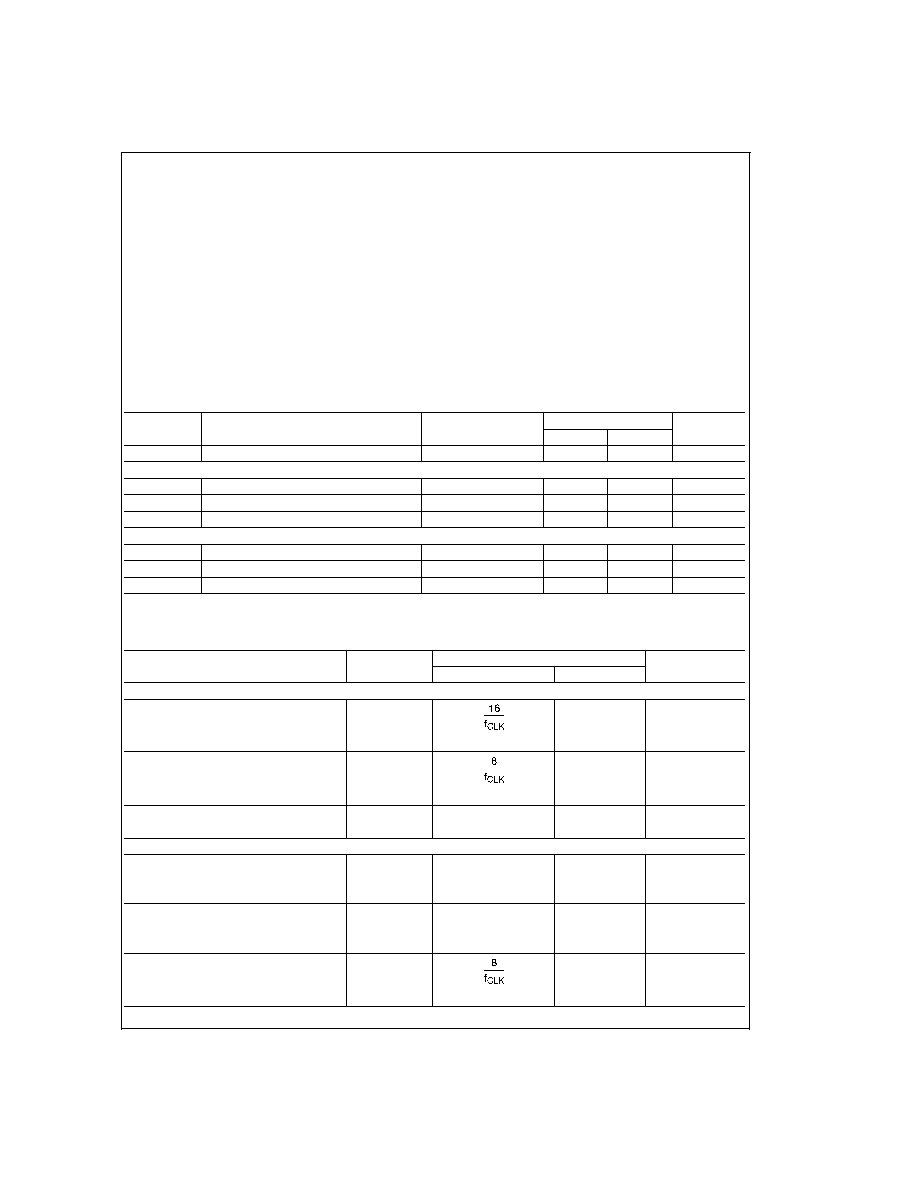
DC Electrical Characteristics
(V
DD
and T
A
per Operating Ratings; f
CLK
= 6 MHz)
Symbol
Parameter
Conditions
Tested Limits
Units
Min
Max
I
DD
Supply Current
Outputs Open
110
mA
INPUT VOLTAGES
V
IH
Logic 1 Input Voltage
2.0
V
V
IL
Logic 0 Input Voltage
0.8
V
I
IN
Input Currents
0
V
IN
V
DD
-10
10
µA
OUTPUT VOLTAGES
V
OH
Logic 1
I
OH
= -1.6 mA
2.4
V
V
OL
Logic 0
I
OL
= 1.6 mA
0.4
V
I
OUT
TRI-STATE
Æ
Output Leakage Current
0
V
OUT
V
DD
-10
10
µA
AC Electrical Characteristics
(V
DD
and T
A
per Operating Ratings; f
CLK
= 6 MHz; C
LOAD
= 50 pF; Input Test Signal t
r
= t
f
= 10 ns)
Timing Interval
T#
Tested Limits
Units
Min
Max
ENCODER AND INDEX TIMING (See
Figure 2)
Motor-Phase Pulse Width
T1
µs
Dwell-Time per State
T2
µs
Index Pulse Setup and Hold
T3
0
µs
(Relative to A and B Low)
CLOCK AND RESET TIMING (See
Figure 3)
Clock Pulse Width
LM628N-6, LM629N-6, LM629M-6
T4
78
ns
LM628N-8, LM629N-8, LM629M-8
T4
57
ns
Clock Period
LM628N-6, LM629N-6, LM629M-6
T5
166
ns
LM628N-8, LM629N-8, LM629M-8
T5
125
ns
Reset Pulse Width
T6
µs
LM628/LM629
www.national.com
3
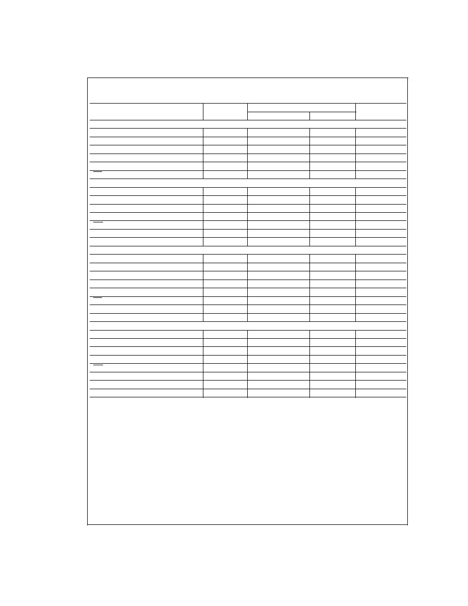
AC Electrical Characteristics
(Continued)
(V
DD
and T
A
per Operating Ratings; f
CLK
= 6 MHz; C
LOAD
= 50 pF; Input Test Signal t
r
= t
f
= 10 ns)
Timing Interval
T#
Tested Limits
Units
Min
Max
STATUS BYTE READ TIMING (See
Figure 4)
Chip-Select Setup/Hold Time
T7
0
ns
Port-Select Setup Time
T8
30
ns
Port-Select Hold Time
T9
30
ns
Read Data Access Time
T10
180
ns
Read Data Hold Time
T11
0
ns
RD High to Hi-Z Time
T12
180
ns
COMMAND BYTE WRITE TIMING (See
Figure 5)
Chip-Select Setup/Hold Time
T7
0
ns
Port-Select Setup Time
T8
30
ns
Port-Select Hold Time
T9
30
ns
Busy Bit Delay
T13
(Note 3)
ns
WR Pulse Width
T14
100
ns
Write Data Setup Time
T15
50
ns
Write Data Hold Time
T16
120
ns
DATA WORD READ TIMING (See
Figure 6)
Chip-Select Setup/Hold Time
T7
0
ns
Port-Select Setup Time
T8
30
ns
Port-Select Hold Time
T9
30
ns
Read Data Access Time
T10
180
ns
Read Data Hold Time
T11
0
ns
RD High to Hi-Z Time
T12
180
ns
Busy Bit Delay
T13
(Note 3)
ns
Read Recovery Time
T17
120
ns
DATA WORD WRITE TIMING (See
Figure 7)
Chip-Select Setup/Hold Time
T7
0
ns
Port-Select Setup Time
T8
30
ns
Port-Select Hold Time
T9
30
ns
Busy Bit Delay
T13
(Note 3)
ns
WR Pulse Width
T14
100
ns
Write Data Setup Time
T15
50
ns
Write Data Hold Time
T16
120
ns
Write Recovery Time
T18
120
ns
Note 1: Absolute Maximum Ratings indicate limits beyond which damage to the device may occur. DC and AC electrical specifications do not apply when operating
the device beyond the above Operating Ratings.
Note 2: When operating at ambient temperatures above 70∞C, the device must be protected against excessive junction temperatures. Mounting the package on a
printed circuit board having an area greater than three square inches and surrounding the leads and body with wide copper traces and large, uninterrupted areas of
copper, such as a ground plane, suffices. The 28-pin DIP (N) and the 24-pin surface mount package (M) are molded plastic packages with solid copper lead frames.
Most of the heat generated at the die flows from the die, through the copper lead frame, and into copper traces on the printed circuit board. The copper traces act
as a heat sink. Double-sided or multi-layer boards provide heat transfer characteristics superior to those of single-sided boards.
Note 3: In order to read the busy bit, the status byte must first be read. The time required to read the busy bit far exceeds the time the chip requires to set the busy
bit. It is, therefore, impossible to test actual busy bit delay. The busy bit is guaranteed to be valid as soon as the user is able to read it.
LM628/LM629
www.national.com
4
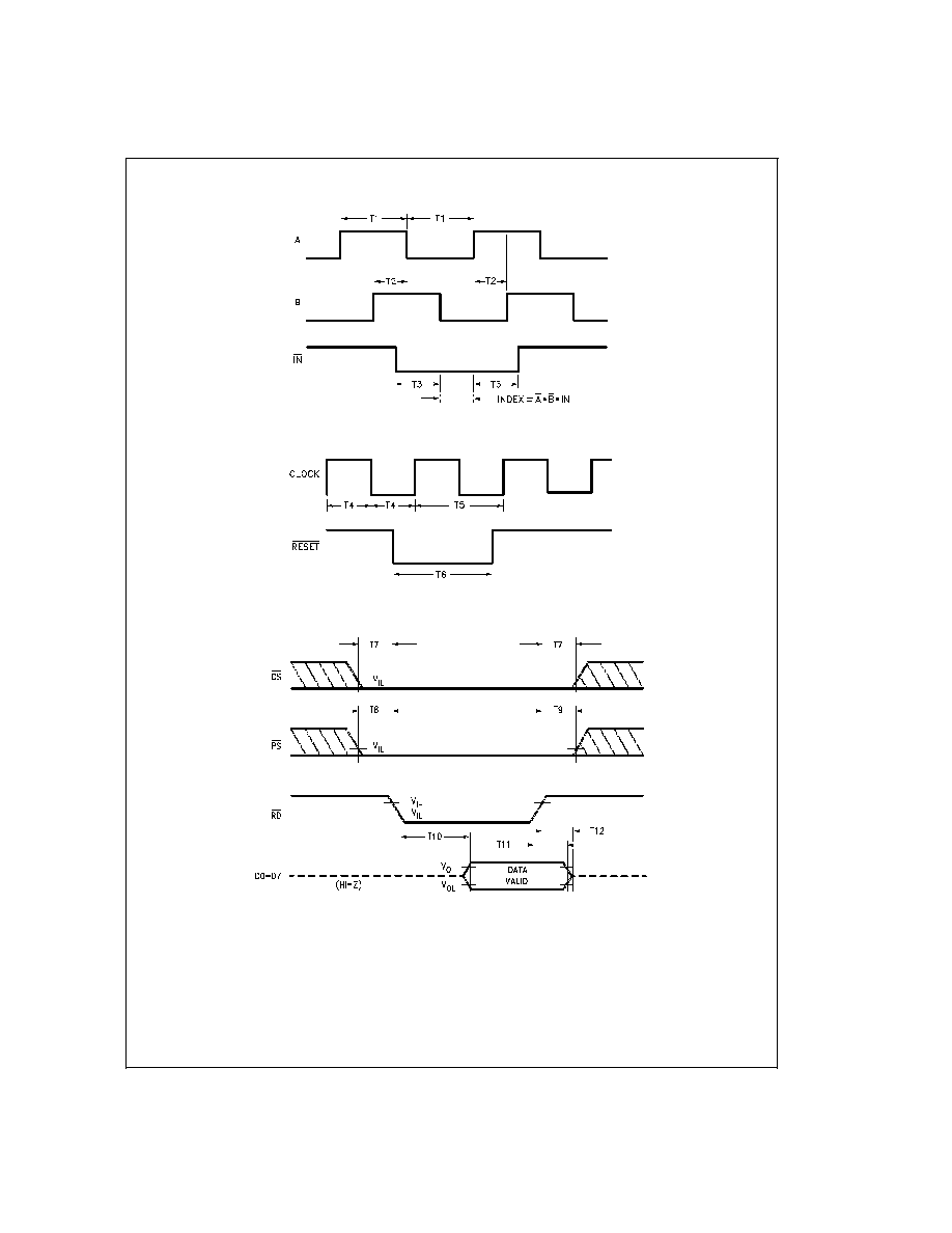
AC Electrical Characteristics
(Continued)
DS009219-4
FIGURE 2. Quadrature Encoder Input Timing
DS009219-5
FIGURE 3. Clock and Reset Timing
DS009219-6
FIGURE 4. Status Byte Read Timing
LM628/LM629
www.national.com
5