TL H 7866
LM733LM733C
Differential
Amplifier
August 1989
LM733 LM733C Differential Amplifier
General Description
The LM733 LM733C is a two-stage differential input differ-
ential output wide-band video amplifier The use of internal
series-shunt feedback gives wide bandwidth with low phase
distortion and high gain stability Emitter-follower outputs
provide a high current drive low impedance capability Its
120 MHz bandwidth and selectable gains of 10 100 and
400 without need for frequency compensation make it a
very useful circuit for memory element drivers pulse amplifi-
ers and wide band linear gain stages
The LM733 is specified for operation over the
b
55 C to
a
125 C military temperature range The LM733C is speci-
fied for operation over the 0 C to
a
70 C temperature range
Features
Y
120 MHz bandwidth
Y
250 kX input resistance
Y
Selectable gains of 10 100 400
Y
No frequency compensation
Y
High common mode rejection ratio at high frequencies
Applications
Y
Magnetic tape systems
Y
Disk file memories
Y
Thin and thick film memories
Y
Woven and plated wire memories
Y
Wide band video amplifiers
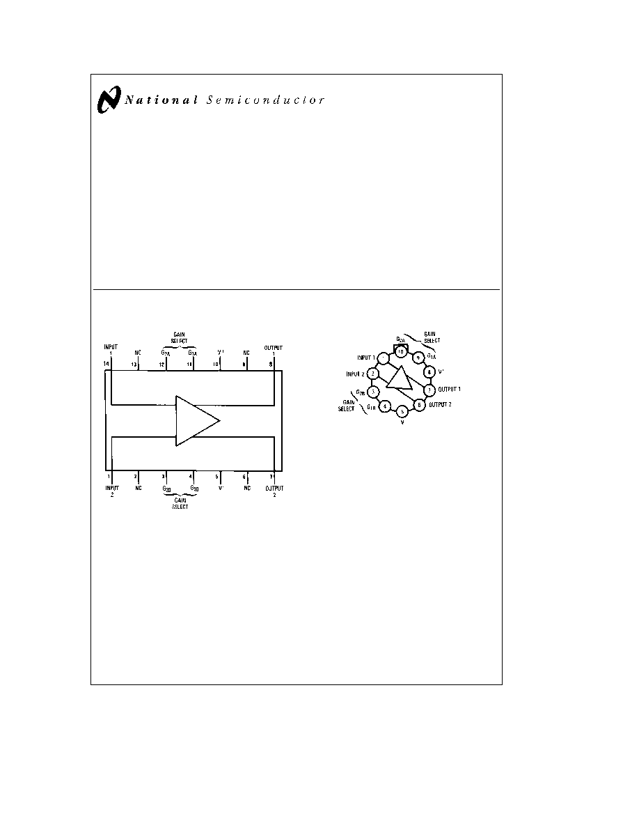
Connection Diagrams
Dual-In-Line Package
TL H 7866 � 1
Top View
Order Number LM733CN
See NS Package Number N14A
Metal Can Package
TL H 7866 � 2
Note
Pin 5 connected to case
Top View
Order Number LM733H or LM733CH
See NS Package Number H10D
C1995 National Semiconductor Corporation
RRD-B30M115 Printed in U S A
Absolute Maximum Ratings
If Military Aerospace specified devices are required
please contact the National Semiconductor Sales
Office Distributors for availability and specifications
Diffential Input Voltage
g
5V
Common Mode Input Voltage
g
6V
V
CC
g
8V
Output Current
10 mA
Power Dissipation (Note 1)
500 mW
Junction Temperature
a
150 C
Storage Temperature Range
b
65 C to
a
150 C
Operating Temperature Range
LM733
b
55 C to
a
125 C
LM733C
0 C to
a
70 C
Lead Temperature (Soldering 10 sec )
260 C
Electrical Characteristics
(T
A
e
25 C unless otherwise specified see test circuits V
S
e
g
6 0V)
Characteristics
Test
Test Conditions
LM733
LM733C
Units
Circuit
Min
Typ
Max
Min
Typ
Max
Differential Voltage Gain
Gain 1 (Note 2)
300
400
500
250
400
600
Gain 2 (Note 3)
1
90
100
110
80
100
120
Gain 3 (Note 4)
R
L
e
2 kX V
OUT
e
3 Vp-p
9 0
10
11
8 0
10
12
Bandwidth
Gain 1
40
40
MHz
Gain 2
2
90
90
MHz
Gain 3
120
120
MHz
Rise Time
Gain 1
V
OUT
e
1 Vp-p
10 5
10 5
ns
Gain 2
2
4 5
10
4 5
12
ns
Gain 3
2 5
2 5
ns
Propagation Delay
V
OUT
e
1 Vp-p
Gain 1
7 5
7 5
ns
Gain 2
2
6 0
10
6 0
10
ns
Gain 3
3 6
3 6
ns
Input Resistance
Gain 1
4 0
4 0
kX
Gain 2
20
30
10
30
kX
Gain 3
250
250
kX
Input Capacitance
Gain 2
2 0
2 0
pF
Input Offset Current
0 4
3 0
0 4
5 0
m
A
Input Bias Current
9 0
20
9 0
30
m
A
Input Noise Voltage
BW
e
1 kHz to 10 MHz
12
12
m
Vrms
Input Voltage Range
1
g
1 0
g
1 0
V
Common Mode Rejection Ratio
Gain 2
1
V
CM
e
g
1V f
s
100 kHz
60
86
60
86
dB
Gain 2
V
CM
e
g
1V f
e
5 MHz
60
60
dB
Supply Voltage Rejection Ratio
Gain 2
1
D
V
S
e
g
0 5V
50
70
50
70
dB
Output Offset Voltage
Gain 1
1
R
L
e
%
0 6
1 5
0 6
1 5
V
Gain 2 and 3
0 35
1 0
0 35
1 5
V
Output Common Mode Voltage
1
R
L
e
%
2 4
2 9
3 4
2 4
2 9
3 4
V
Output Voltage Swing
1
R
L
e
2k
3 0
4 0
3 0
4 0
Output Sink Current
2 5
3 6
2 5
3 6
mA
Output Resistance
20
20
X
Power Supply Current
1
R
L
e
%
18
24
18
24
mA
2

Electrical Characteristics
(Continued)
(The following specifications apply for
b
55 C
k
T
A
k
125 C for the LM733 and 0 C
k
T
A
k
70 C for the LM733C V
S
e
g
6 0V)
Characteristics
Test
Test Conditions
LM733
LM733C
Units
Circuit
Min
Typ
Max
Min
Typ
Max
Differential Voltage Gain
Gain 1
200
600
250
600
Gain 2
1
R
L
e
2 kX V
OUT
e
3 Vp-p
80
120
80
120
Gain 3
8 0
12 0
8 0
12 0
Input Resistance Gain 2
8
8
kX
Input Offset Current
5
6
m
A
Input Bias Current
40
40
m
A
Input Voltage Range
1
g
1
g
1
V
Common Mode Rejection Ratio
Gain 2
1
V
CM
e
g
1V f
s
100 kHz
50
50
dB
Supply Voltage Rejection Ratio
Gain 2
1
D
V
S
e
g
0 5V
50
50
dB
Output Offset Voltage
Gain 1
1
R
L
e
%
1 5
1 5
V
Gain 2 and 3
1 2
1 5
V
Output Voltage Swing
1
R
L
e
2k
2 5
2 8
V
pp
Output Sink Current
2 2
2 5
mA
Power Supply Current
1
R
L
e
%
27
27
mA
Note 1
The maximum junction temperature of the LM733 is 150 C while that of the LM733C is 100 C For operation at elevated temperatures devices in the TO-
100 package must be derated based on a thermal resistance of 150 C W junction to ambient or 45 C W junction to case Thermal resistance of the dual-in-line
package is 90 C W
Note 2
Pins G1A and G1B connected together
Note 3
Pins G2A and G2B connected together
Note 4
Gain select pins open
Note 5
Refer to RETS733X drawing for specifications of LM733H version
Typical Performance Characteristics
Pulse Response
Temperature
Pulse Response vs
Supply Voltage
Pulse Response vs
vs Frequency
Phase Shift
vs Frequency
Phase Shift
Recovery Time
Differential Overdrive
TL H 7866 � 6
3
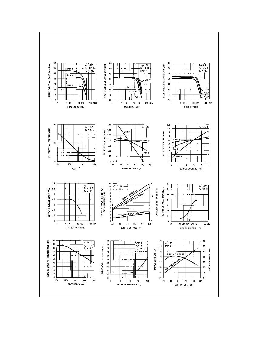
Typical Performance Characteristics
(Continued)
Voltage Gain vs Frequency
Temperature
Gain vs Frequency
Supply Voltage
Gain vs Frequency vs
Voltage Gain vs R
ADJ
Voltage Gain vs Temperature
Supply Voltage
Voltage Gain vs
Frequency
Output Voltage Swing vs
Voltage
and Current Swing vs Supply
Supply Current Output Voltage
Load Resistance
Output Voltage Swing vs
Ratio vs Frequency
Common Mode Rejection
Source Resistance
Input Noise Voltage vs
Resistance vs Temperature
Supply Current and Input
TL H 7866 � 7
4
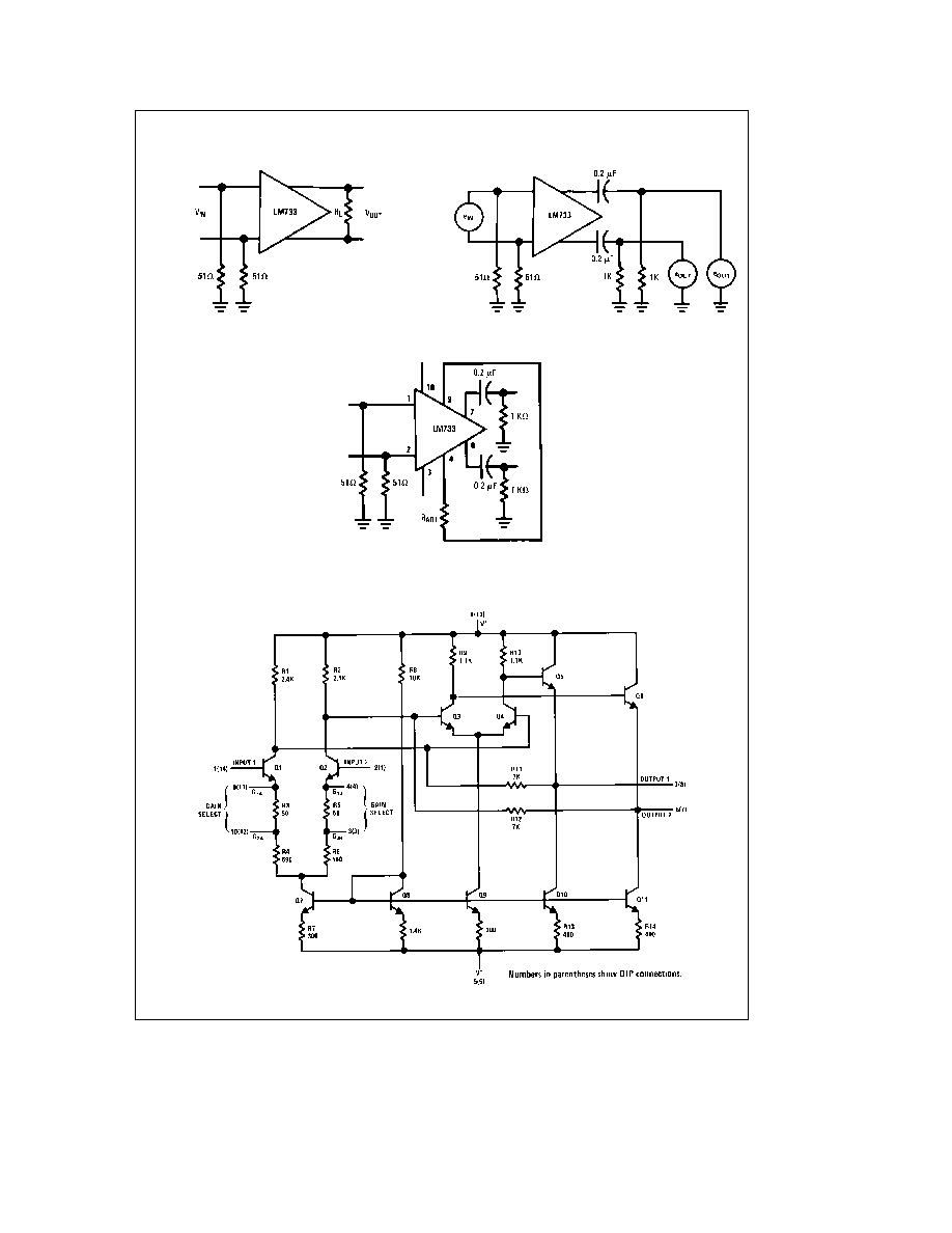
Test Circuits
Test Circuit 1
TL H 7866 � 3
Test Circuit 2
TL H 7866 � 4
Voltage Gain Adjust Circuit
TL H 7866 � 5
V
S
e
6V T
A
e
25 C
(Pin numbers apply to TO-5 package)
Schematic Diagram
TL H 7866 � 8
5
LM733LM733C
Differential
Amplifier
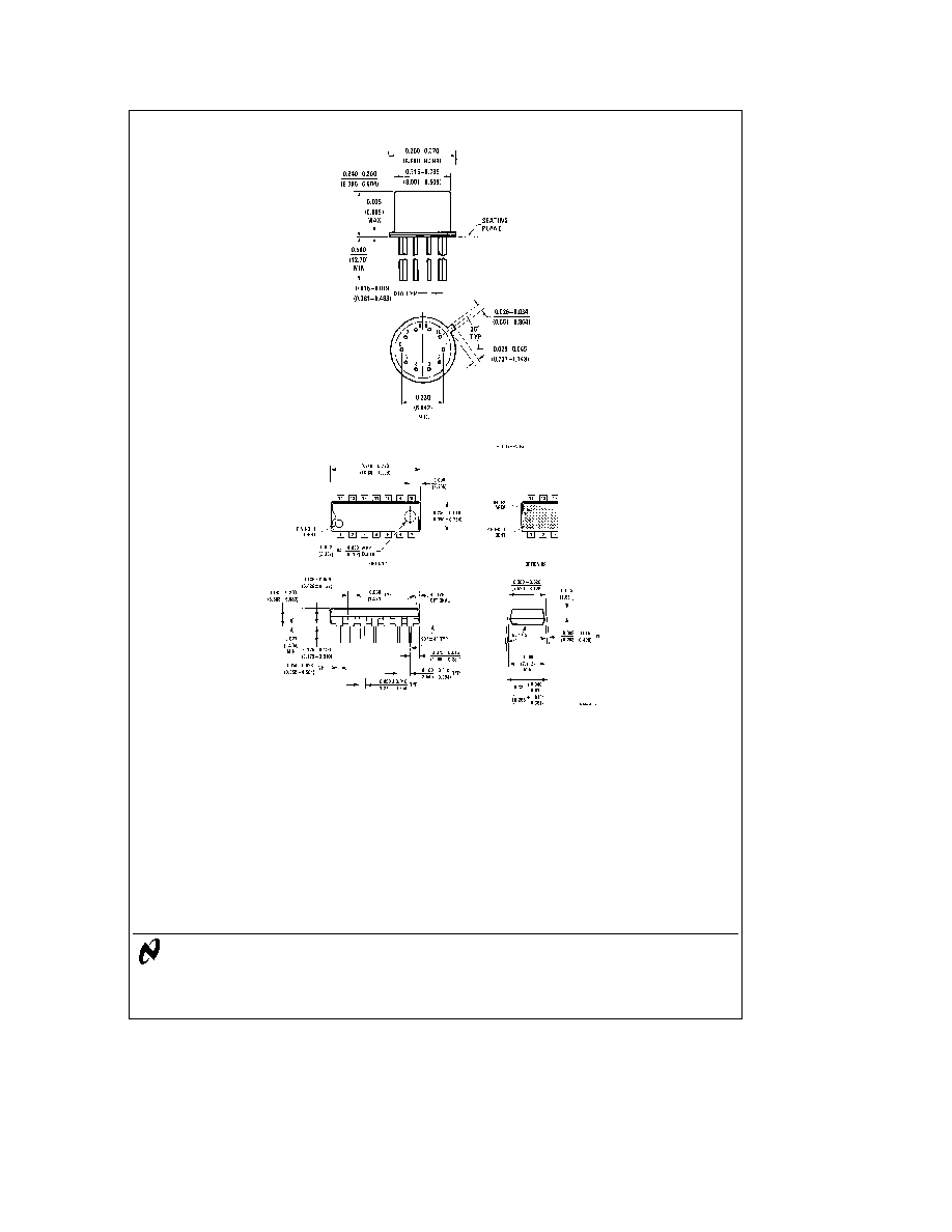
Physical Dimensions
inches (millimeters)
Metal Can Package (H)
Order Number LM733H or LM733CH
NS Package Number H10D
Molded Dual-In-Line Package (N)
Order Number LM733CN
NS Package Number N14A
LIFE SUPPORT POLICY
NATIONAL'S PRODUCTS ARE NOT AUTHORIZED FOR USE AS CRITICAL COMPONENTS IN LIFE SUPPORT
DEVICES OR SYSTEMS WITHOUT THE EXPRESS WRITTEN APPROVAL OF THE PRESIDENT OF NATIONAL
SEMICONDUCTOR CORPORATION As used herein
1 Life support devices or systems are devices or
2 A critical component is any component of a life
systems which (a) are intended for surgical implant
support device or system whose failure to perform can
into the body or (b) support or sustain life and whose
be reasonably expected to cause the failure of the life
failure to perform when properly used in accordance
support device or system or to affect its safety or
with instructions for use provided in the labeling can
effectiveness
be reasonably expected to result in a significant injury
to the user
National Semiconductor
National Semiconductor
National Semiconductor
National Semiconductor
Corporation
Europe
Hong Kong Ltd
Japan Ltd
1111 West Bardin Road
Fax (a49) 0-180-530 85 86
13th Floor Straight Block
Tel 81-043-299-2309
Arlington TX 76017
Email cnjwge tevm2 nsc com
Ocean Centre 5 Canton Rd
Fax 81-043-299-2408
Tel 1(800) 272-9959
Deutsch Tel (a49) 0-180-530 85 85
Tsimshatsui Kowloon
Fax 1(800) 737-7018
English
Tel (a49) 0-180-532 78 32
Hong Kong
Fran ais Tel (a49) 0-180-532 93 58
Tel (852) 2737-1600
Italiano
Tel (a49) 0-180-534 16 80
Fax (852) 2736-9960
National does not assume any responsibility for use of any circuitry described no circuit patent licenses are implied and National reserves the right at any time without notice to change said circuitry and specifications