 | –≠–ª–µ–∫—Ç—Ä–æ–Ω–Ω—ã–π –∫–æ–º–ø–æ–Ω–µ–Ω—Ç: LM8333 | –°–∫–∞—á–∞—Ç—å:  PDF PDF  ZIP ZIP |
LM8333
Keypad Controller with I/O Expansion and ACCESS.bus
Host Interface
1.0 General Description
The LM8333 is a general-purpose controller for matrix-
addressed keypads which provides an ACCESS.bus (I
2
C-
compatible) interface to a host microcontroller. It offloads the
burden of keyboard scanning from the host, while providing
extremely low power consumption in both operational and
standby modes. It supports keypad matrices up to 8 x 8 in
size (plus another 8 special-function keys), for portable ap-
plications such as cellphones, PDAs, games, and other
handheld applications.
Key press and release events are encoded into a byte format
and loaded into a FIFO buffer for retrieval by the host pro-
cessor. An interrupt output (IRQ) is used to signal events
such as keypad activity, a state change on either of two
interrupt-capable general-purpose I/O pins, or an error con-
dition. Interrupt and error codes are available to the host by
reading dedicated registers.
Four general-purpose I/O pins are available, two of which
have interrupt capability. A pulse-width modulated output
based on a host-programmable internal timer is also avail-
able, which can be used as a general-purpose output if the
PWM function is not required.
To minimize power, the LM8333 automatically enters a low-
power standby mode when there is no keypad, I/O, or host
activity.
The device is packaged in a 49-pin MICRO-ARRAY chip-
scale package.
2.0 Features
n
8 x 8 standard keys
n
8 special function keys (SF keys) providing a total of 72
keys for the maximum keyboard matrix
n
ACCESS.bus (I
2
C-compatible) communication interface
to the host
n
Four general purpose host programmable I/O pins with
two optional (slow) external Interrupts
n
16 byte FIFO buffer to store key pressed and key
released events
n
Error control with error reports on (FIFO overrun,
Keypad overrun, invalid command)
n
Host programmable PWM
n
Host programmable active time and debounce time
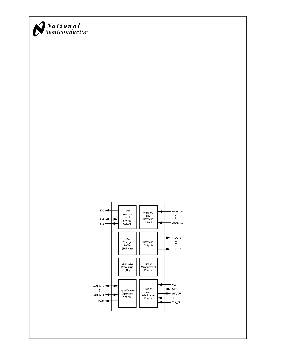
3.0 Block Diagram
20210601
September 2006
LM8333
Keypad
Controller
with
I/O
Expansion
and
ACCESS.bus
Host
Interface
© 2006 National Semiconductor Corporation
DS202106
www.national.com

4.0 Pin Assignments
20210602
Top View
49-Pin MICRO-ARRAY
See NS Package Number GRA49A
LM8333
www.national.com
2

Table of Contents
1.0 General Description ..................................................................................................................................... 1
2.0 Features ....................................................................................................................................................... 1
3.0 Block Diagram .............................................................................................................................................. 1
4.0 Pin Assignments ........................................................................................................................................... 2
5.0 Signal Descriptions ...................................................................................................................................... 4
6.0 Typical Application ........................................................................................................................................ 5
6.1 I/O EXPANSION OPTIONS ....................................................................................................................... 5
6.2 WATCHDOG TIMER ................................................................................................................................. 5
6.3 HALT MODE .............................................................................................................................................. 5
6.3.1 ACCESS.bus Activity ........................................................................................................................... 5
6.4 KEYPAD SCANNING ................................................................................................................................ 6
6.5 COMMUNICATION INTERFACE .............................................................................................................. 6
6.5.1 Interrupts Between the Host and LM8333 .......................................................................................... 6
6.5.2 Interrupt Sources ................................................................................................................................. 6
7.0 Device Operation ......................................................................................................................................... 6
7.1 EVENT CODE ASSIGNMENT .................................................................................................................. 6
7.2 I/O EXPANSION ........................................................................................................................................ 7
7.2.1 PWM Output with Programmable Duty Cycle ..................................................................................... 7
7.2.2 General-Purpose I/O (GPIO) ............................................................................................................... 8
7.2.3 External Interrupts ............................................................................................................................... 9
7.3 HOST COMMAND EXECUTION ............................................................................................................ 10
7.3.1 Command Structure ........................................................................................................................... 10
7.4 HOST WRITE COMMANDS ................................................................................................................... 10
7.5 HOST READ COMMANDS ..................................................................................................................... 10
7.6 WAKE-UP FROM HALT MODE .............................................................................................................. 11
8.0 Interrupts .................................................................................................................................................... 12
8.1 INTERRUPT CODE ................................................................................................................................. 12
8.2 ERROR CODE ........................................................................................................................................ 12
8.3 STATUS CODES ..................................................................................................................................... 12
8.4 INTERRUPT PROCESSING ................................................................................................................... 12
8.5 COMMAND EXECUTION SUMMARY .................................................................................................... 13
9.0 Electrical Characteristics ............................................................................................................................ 14
10.0 Absolute Maximum Ratings ..................................................................................................................... 14
11.0 DC Electrical Characteristics .................................................................................................................... 14
12.0 AC Electrical Characteristics .................................................................................................................... 15
13.0 Physical Dimensions ................................................................................................................................ 17
LM8333
www.national.com
3

5.0 Signal Descriptions
Name
Pin
I/O
Description
WAKE_IN0
D7
Input
Wake-up input/Keyboard scanning input 0
WAKE_IN1
C7
Input
Wake-up input/Keyboard scanning input 1
WAKE_IN2
E7
Input
Wake-up input/Keyboard scanning input 2
WAKE_IN3
D6
Input
Wake-up input/Keyboard scanning input 3
WAKE_IN4
B6
Input
Wake-up input/Keyboard scanning input 4
WAKE_IN5
A7
Input
Wake-up input/Keyboard scanning input 5
WAKE_IN6
A6
Input
Wake-up input/Keyboard scanning input 6
WAKE_IN7
B5
Input
Wake-up input/Keyboard scanning input 7
K_OUT0
G3
Output
Keyboard scanning output 0
K_OUT1
F4
Output
Keyboard scanning output 1
K_OUT2
G4
Output
Keyboard scanning output 2
K_OUT3
G5
Output
Keyboard scanning output 3
K_OUT4
A5
Output
Keyboard scanning output 4
K_OUT5
B4
Output
Keyboard scanning output 5
K_OUT6
A4
Output
Keyboard scanning output 6
K_OUT7
A3
Output
Keyboard scanning output 7
GEN_IO_0
D2
I/O
General-purpose I/O 0
GEN_IO_1
D1
I/O
General-purpose I/O 1
GEN_IO_2
B3
I/O
General-purpose I/O 2
GEN_IO_3
A2
I/O
General-purpose I/O 3
SDA
F7
I/O
ACCESS.bus data signal
SCL
E6
I/O
ACCESS.bus clock signal
IRQ
F2
Output
Interrupt request output
PWM
F1
Output
Pulse-width modulated output
WD_OUT
G1
Output
Watchdog timer output (connect to RESET input)
RESET
F3
Input
Reset input
CLK_IN
B1
Input
Clock input (connect to ground through a 68k ohm resistor)
VCC
E1, E2
n.a.
Vcc
GND
A1, B2, C3, C4,
C5, D3, D4, D5,
E3, E4, E5
n.a.
Ground
NC
B7, C1, C2, C6,
F5, F6, G2, G6,
G7
n.a.
No connect
LM8333
www.national.com
4

6.0 Typical Application
6.1 I/O EXPANSION OPTIONS
∑
One host-programmable PWM output which also may be
used as a general-purpose output.
∑
Four host-programmable general-purpose I/O pins, GE-
N_IO_0, GEN_IO_1, GEN_IO_2, and GEN_IO_3. GE-
N_IO_0 and GEN_IO_1 can also be configured for "slow"
interrupts, in which any transition will trigger a hardware
interrupt event to the host.
6.2 WATCHDOG TIMER
The watchdog timer is always enabled in hardware. To use
the timer, connect the WD_OUT output to the RESET input.
6.3 HALT MODE
The fully static architecture of the LM8333 allows stopping
the internal RC clock in Halt mode, which reduces power
consumption to the minimum level.
Halt mode is entered when no key-press, key-release, or
ACCESS.bus activity is detected for a certain period of time
(by default, 500 milliseconds). The mechanism for entering
Halt mode is always enabled in hardware, but the host can
program the period of inactivity which triggers entry into Halt
mode.
The LM8333 will remain in Active mode as long as a key
event, or any other event, which causes the IRQ output to be
asserted is not resolved.
6.3.1 ACCESS.bus Activity
When the LM8333 is in Halt mode, any activity on the
ACCESS.bus interface will cause the LM8333 to exit from
Halt mode. However, the LM8333 will not be able to ac-
knowledge the first bus cycle immediately following wake-up
from Halt mode. It will respond with a negative acknowledge-
ment, and the host should then repeat the cycle.
The LM8333 will be prevented from entering Halt mode if it
shares the bus with peripherals that are continuously active.
For lowest power consumption, the LM8333 should only
share the bus with peripherals that require little or no bus
activity after system initialization.
20210603
FIGURE 1. Typical Keypad Configuration
LM8333
www.national.com
5