 | –≠–ª–µ–∫—Ç—Ä–æ–Ω–Ω—ã–π –∫–æ–º–ø–æ–Ω–µ–Ω—Ç: LM95221 | –°–∫–∞—á–∞—Ç—å:  PDF PDF  ZIP ZIP |

LM95221
Dual Remote Diode Digital Temperature Sensor with
SMBus Interface
General Description
The LM95221 is a dual remote diode temperature sensor in
an 8-lead MSOP package. The 2-wire serial interface of the
LM95221 is compatible with SMBus 2.0. The LM95221 can
sense three temperature zones, it can measure the tempera-
ture of its own die as well as two diode connected transis-
tors. The diode connected transistors can be a thermal diode
as found in Pentium and AMD processors or can simply be a
diode connected MMBT3904 transistor. The LM95221 reso-
lution format for remote temperature readings can be pro-
grammed to be 10-bits plus sign or 11-bits unsigned. In the
unsigned mode the LM95221 remote diode readings can
resolve temperatures above 127∞C. Local temperature read-
ings have a resolution of 9-bits plus sign.
The temperature of any ASIC can be accurately determined
using the LM95221 as long as a dedicated diode (semicon-
ductor junction) is available on the target die. The LM95221
remote sensor accuracy of
±
1∞C is factory trimmed for a
series resistance of 2.7 ohms and 1.008 non-ideality factor.
Features
n
Accurately senses die temperature of remote ICs or
diode junctions
n
Remote diode fault detection
n
On-board local temperature sensing
n
Remote temperature readings:
-- 0.125 ∞C LSb
-- 10-bits plus sign or 11-bits programmable resolution
-- 11-bits resolves temperatures above 127 ∞C
n
Local temperature readings:
-- 0.25 ∞C
-- 9-bits plus sign
n
Status register support
n
Programmable conversion rate allows user optimization
of power consumption
n
Shutdown mode one-shot conversion control
n
SMBus 2.0 compatible interface, supports TIMEOUT
n
8-pin MSOP package
Key Specifications
j
Local Temperature Accuracy
T
A
=0∞C to 85∞C
±
3.0 ∞C (max)
j
Remote Diode Temperature Accuracy
T
A
=30∞C to 50∞C, T
D
=45∞C to 85∞C
±
1.0 ∞C (max)
T
A
=0∞C to 85∞C, T
D
=25∞C to 140∞C
±
3.0 ∞C (max)
j
Supply Voltage
3.0 V to 3.6 V
j
Supply Current
2 mA (typ)
Applications
n
Processor/Computer System Thermal Management
(e.g. Laptop, Desktop, Workstations, Server)
n
Electronic Test Equipment
n
Office Electronics
Simplified Block Diagram
20094301
Pentium
TM
is a trademark of Intel Corporation.
May 2004
LM95221
Dual
Remote
Diode
Digital
T
emperature
Sensor
with
SMBus
Interface
© 2004 National Semiconductor Corporation
DS200943
www.national.com

Connection Diagram
MSOP-8
20094302
TOP VIEW
Ordering Information
Part Number
Package
Marking
NS Package
Number
Transport
Media
SMBus Device
Address
LM95221CIMM
LM95221CIMM
MUA08A (MSOP-8)
1000 Units on Tape
and Reel
010 1011
LM95221CIMMX
LM95221CIMM
MUA08A (MSOP-8)
3500 Units on Tape
and Reel
010 1011
Pin Descriptions
Label
Pin #
Function
Typical Connection
D1+
1
Diode Current Source
To Diode Anode. Connected to remote discrete
diode-connected transistor junction or to the
diode-connected transistor junction on a remote IC
whose die temperature is being sensed. A 2.2 nF
diode bypass capacitor is recommended to filter high
frequency noise. Place the 2.2 nF capacitor between
and as close as possible to the LM95221's D+ and
D- pins. Make sure the traces to the 2.2 nF
capacitor are matched. Ground this pin if this
thermal diode is not used.
D1-
2
Diode Return Current Sink
To Diode Cathode. A 2.2 nF capacitor is
recommended between D1+ and D1-. Ground this
pin if this thermal diode is not used.
D2+
3
Diode Current Source
To Diode Anode. Connected to remote discrete
diode-connected transistor junction or to the
diode-connected transistor junction on a remote IC
whose die temperature is being sensed. A 2.2 nF
diode bypass capacitor is recommended to filter high
frequency noise. Place the 2.2 nF capacitor between
and as close as possible to the LM95221's D+ and
D- pins. Make sure the traces to the 2.2 nF
capacitor are matched. Ground this pin if this
thermal diode is not used.
D2-
4
Diode Return Current Sink
To Diode Cathode. A 2.2 nF capacitor is
recommended between D2+ and D2-. Ground this
pin if this thermal diode is not used.
GND
5
Power Supply Ground
Ground
V
DD
6
Positive Supply Voltage
Input
DC Voltage from 3.0 V to 3.6 V. V
DD
should be
bypassed with a 0.1 µF capacitor in parallel with 100
pF. The 100 pF capacitor should be placed as close
as possible to the power supply pin. Noise should
be kept below 200 mVp-p, a 10 µF capacitor may be
required to achieve this.
LM95221
www.national.com
2
Pin Descriptions
(Continued)
Label
Pin #
Function
Typical Connection
SMBDAT
7
SMBus Bi-Directional Data
Line, Open-Drain Output
From and to Controller; may require an external
pull-up resistor
SMBCLK
8
SMBus Clock Input
From Controller; may require an external pull-up
resistor
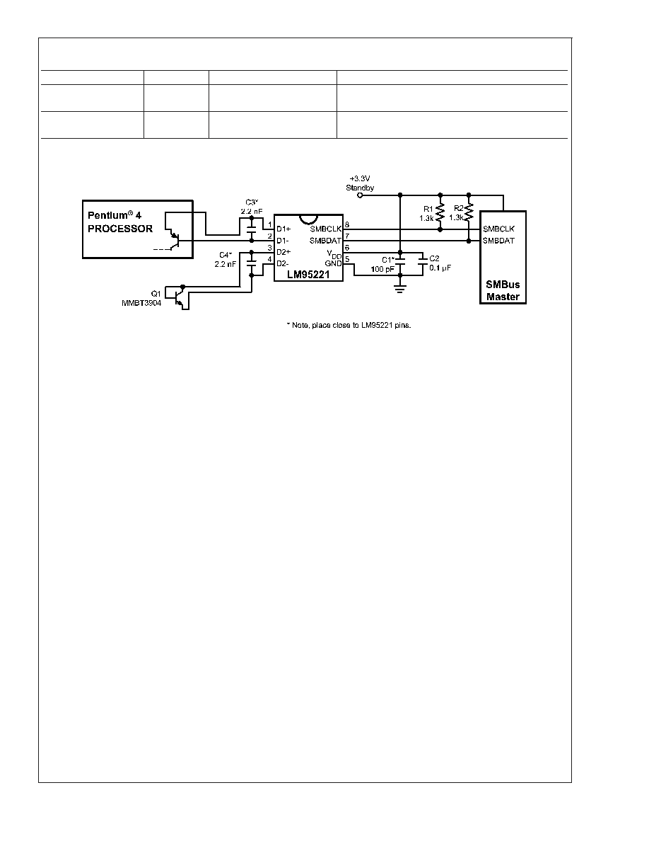
Typical Application
20094303
LM95221
www.national.com
3

Absolute Maximum Ratings
(Note 1)
Supply Voltage
-0.3 V to 6.0 V
Voltage at SMBDAT, SMBCLK
-0.5V to 6.0V
Voltage at Other Pins
-0.3 V to (V
DD
+ 0.3 V)
D- Input Current
±
1 mA
Input Current at All Other Pins (Note 2)
±
5 mA
Package Input Current (Note 2)
30 mA
SMBDAT Output Sink Current
10 mA
Storage Temperature
-65∞C to +150∞C
Soldering Information, Lead Temperature
MSOP-8 Package (Note 3)
Vapor Phase (60 seconds)
215∞C
Infrared (15 seconds)
220∞C
ESD Susceptibility (Note 4)
Human Body Model
2000 V
Machine Model
200 V
Operating Ratings
(Notes 1, 5)
Operating Temperature Range
0∞C to +115∞C
Electrical Characteristics
Temperature Range
T
MIN
T
A
T
MAX
LM95221CIMM
0∞C
T
A
+85∞C
Supply Voltage Range (V
DD
)
+3.0V to +3.6V
Temperature-to-Digital Converter Characteristics
Unless otherwise noted, these specifications apply for V
DD
=+3.0Vdc to 3.6Vdc. Boldface limits apply for T
A
= T
J
=
T
MIN
T
A
T
MAX
; all other limits T
A
= T
J
=+25∞C, unless otherwise noted. T
J
is the junction temperature of the LM95221. T
D
is the
junction temperature of the remote thermal diode.
Parameter
Conditions
Typical
Limits
Units
(Note 6)
(Note 7)
(Limit)
Accuracy Using Local Diode
T
A
= 0∞C to +85∞C, (Note 8)
±
1
±
3
∞C (max)
Accuracy Using Remote Diode, see (Note 9) for
Thermal Diode Processor Type.
T
A
= +30∞C to
+50∞C
T
D
= +45∞C
to +85∞C
±
1
∞C (max)
T
A
= +0∞C to
+85∞C
T
D
= +25∞C
to +140∞C
±
3
∞C (max)
Remote Diode Measurement Resolution
11
Bits
0.125
∞C
Local Diode Measurement Resolution
10
Bits
0.25
∞C
Conversion Time of All Temperatures at the
Fastest Setting
(Note 11)
66
73
ms (max)
Quiescent Current (Note 10)
SMBus Inactive, 15Hz conversion
rate
2.0
2.6
mA (max)
Shutdown
335
µA
D- Source Voltage
0.7
V
Diode Source Current
(D+ - D-)=+ 0.65V; high-level
188
315
µA (max)
110
µA (min)
Low-level
11.75
20
µA (max)
7
µA (min)
Low-Level Diode Source Current Variation over
Temperature
T
A
= +30∞C to +50∞C
+0.5
µA
T
A
= +30∞C to +85∞C
+1.5
µA
Power-On Reset Threshold
Measure on V
DD
input, falling
edge
2.4
1.8
V (max)
V (min)
LM95221
www.national.com
4

Logic Electrical Characteristics
DIGITAL DC CHARACTERISTICS Unless otherwise noted, these specifications apply for V
DD
=+3.0 to 3.6 Vdc. Boldface lim-
its apply for T
A
= T
J
= T
MIN
to T
MAX
; all other limits T
A
= T
J
=+25∞C, unless otherwise noted.
Symbol
Parameter
Conditions
Typical
Limits
Units
(Note 6)
(Note 7)
(Limit)
SMBDAT, SMBCLK INPUTS
V
IN(1)
Logical "1" Input Voltage
2.1
V (min)
V
IN(0)
Logical "0"Input Voltage
0.8
V (max)
V
IN(HYST)
SMBDAT and SMBCLK Digital Input
Hysteresis
400
mV
I
IN(1)
Logical "1" Input Current
V
IN
= V
DD
0.005
±
10
µA (max)
I
IN(0)
Logical "0" Input Current
V
IN
= 0 V
-0.005
±
10
µA (max)
C
IN
Input Capacitance
5
pF
SMBDAT OUTPUT
I
OH
High Level Output Current
V
OH
= V
DD
10
µA (max)
V
OL
SMBus Low Level Output Voltage
I
OL
= 4mA
I
OL
= 6mA
0.4
0.6
V (max)
SMBus DIGITAL SWITCHING CHARACTERISTICS Unless otherwise noted, these specifications apply for V
DD
=+3.0 Vdc to
+3.6 Vdc, C
L
(load capacitance) on output lines = 80 pF. Boldface limits apply for T
A
= T
J
= T
MIN
to T
MAX
; all other limits T
A
= T
J
= +25∞C, unless otherwise noted. The switching characteristics of the LM95221 fully meet or exceed the published specifi-
cations of the SMBus version 2.0. The following parameters are the timing relationships between SMBCLK and SMBDAT sig-
nals related to the LM95221. They adhere to but are not necessarily the SMBus bus specifications.
Symbol
Parameter
Conditions
Typical
Limits
Units
(Note 6)
(Note 7)
(Limit)
f
SMB
SMBus Clock Frequency
100
10
kHz (max)
kHz (min)
t
LOW
SMBus Clock Low Time
from V
IN(0)
max to V
IN(0)
max
4.7
25
µs (min)
ms (max)
t
HIGH
SMBus Clock High Time
from V
IN(1)
min to V
IN(1)
min
4.0
µs (min)
t
R,SMB
SMBus Rise Time
(Note 12)
1
µs (max)
t
F,SMB
SMBus Fall Time
(Note 13)
0.3
µs (max)
t
OF
Output Fall Time
C
L
= 400pF,
I
O
= 3mA, (Note 13)
250
ns (max)
t
TIMEOUT
SMBDAT and SMBCLK Time Low for Reset of
Serial Interface (Note 14)
25
35
ms (min)
ms (max)
t
SU;DAT
Data In Setup Time to SMBCLK High
250
ns (min)
t
HD;DAT
Data Out Stable after SMBCLK Low
300
900
ns (min)
ns (max)
t
HD;STA
Start Condition SMBDAT Low to SMBCLK
Low (Start condition hold before the first clock
falling edge)
100
ns (min)
t
SU;STO
Stop Condition SMBCLK High to SMBDAT
Low (Stop Condition Setup)
100
ns (min)
t
SU;STA
SMBus Repeated Start-Condition Setup Time,
SMBCLK High to SMBDAT Low
0.6
µs (min)
t
BUF
SMBus Free Time Between Stop and Start
Conditions
1.3
µs (min)
LM95221
www.national.com
5