 | –≠–ª–µ–∫—Ç—Ä–æ–Ω–Ω—ã–π –∫–æ–º–ø–æ–Ω–µ–Ω—Ç: LM9830 | –°–∫–∞—á–∞—Ç—å:  PDF PDF  ZIP ZIP |
1
http://www.national.com
General Description
The LM9830 is a complete document scanner system on a sin-
gle IC. The LM9830 provides all the functions (CCD control, illu-
mination control, analog front end, pixel processing function
image data buffer/SRAM controller, microstepping motor control-
ler, and EPP parallel port interface) necessary to create a high
performance color scanner. The LM9830 scans images in 36 bit
color, and has output data formats for 36 bits, 30 bits, and 24
bits.
The only additional active components required are an external
SRAM for data buffering and power transistors for the stepper
motor. Parallel port pass-through requires two additional
TTL/CMOS logic ICs.
Applications
∑
Color Flatbed Document Scanners
∑
Color Sheetfed Document Scanners
Features
∑ Scans at up to 6Mpixels/s (2M RGB pixels/sec).
∑ Digital Pixel Processing provides 300, 200, 150, 100, 75, and
50 dpi horizontal resolution from 300dpi sensor, and 600, 400,
300, 200, 150, 100, 75, and 50 dpi horizontal resolution from
a 600dpi sensor.
∑ Provides 50-600dpi vertical resolution in 1 dpi increments.
∑ Pixel rate error correction for gain (shading) and offset errors.
∑ Output formats include 12 bit linear, 10 bit linear with shading
and offset, or 8 bit gamma corrected, all with 12 bit accuracy.
∑ Multiple CCD clocking rates allows matching of CCD clock to
scan resolution and pixel depth for maximum scan speed.
∑ Stepper motor control tightly coupled with buffer management
to maximize data transfer efficiency.
∑ PWM stepper motor current control allows microstepping for
the price of fullstepping.
∑ Supports 64k, 128k, or 256k x8 external SRAMs.
∑ Parallel Port interface supports EPP, PS2 (bidirectional), or
SPP (nibble) modes of operation.
∑ Pixel depths of 1, 2, or 4 bits are packed into bytes for faster
scans of line art and low pixel depth images.
∑ Supports 1 and 3 channel CIS and CCD devices.
∑ 3 (R, G, and B) user-programmable gamma correction tables.
∑ Able to transmit an arbitrary range of pixels to speed up
scanning of smaller items (business cards, etc.) by zooming
in on a subset of CCD pixels.
∑ Compatible with a wide range of color linear CCDs and
Contact Image Sensors (CIS)
∑ Internal bandgap voltage reference.
∑ 100 pin TQFP package
Key Specifications
∑
Analog to Digital Converter Resolution
12 Bits
∑
Maximum Pixel Conversion Rate
6MHz
∑
A4 Color 150dpi scan (typical, EPP Interface)
<10 seconds
∑
A4 Color 300dpi scan (typical, EPP Interface)
<40 seconds
∑
A4 Color 600dpi scan (typical, EPP Interface) <160 seconds
∑
Supply Voltage
+5V±10%
∑
Power Dissipation (typical)
350mW
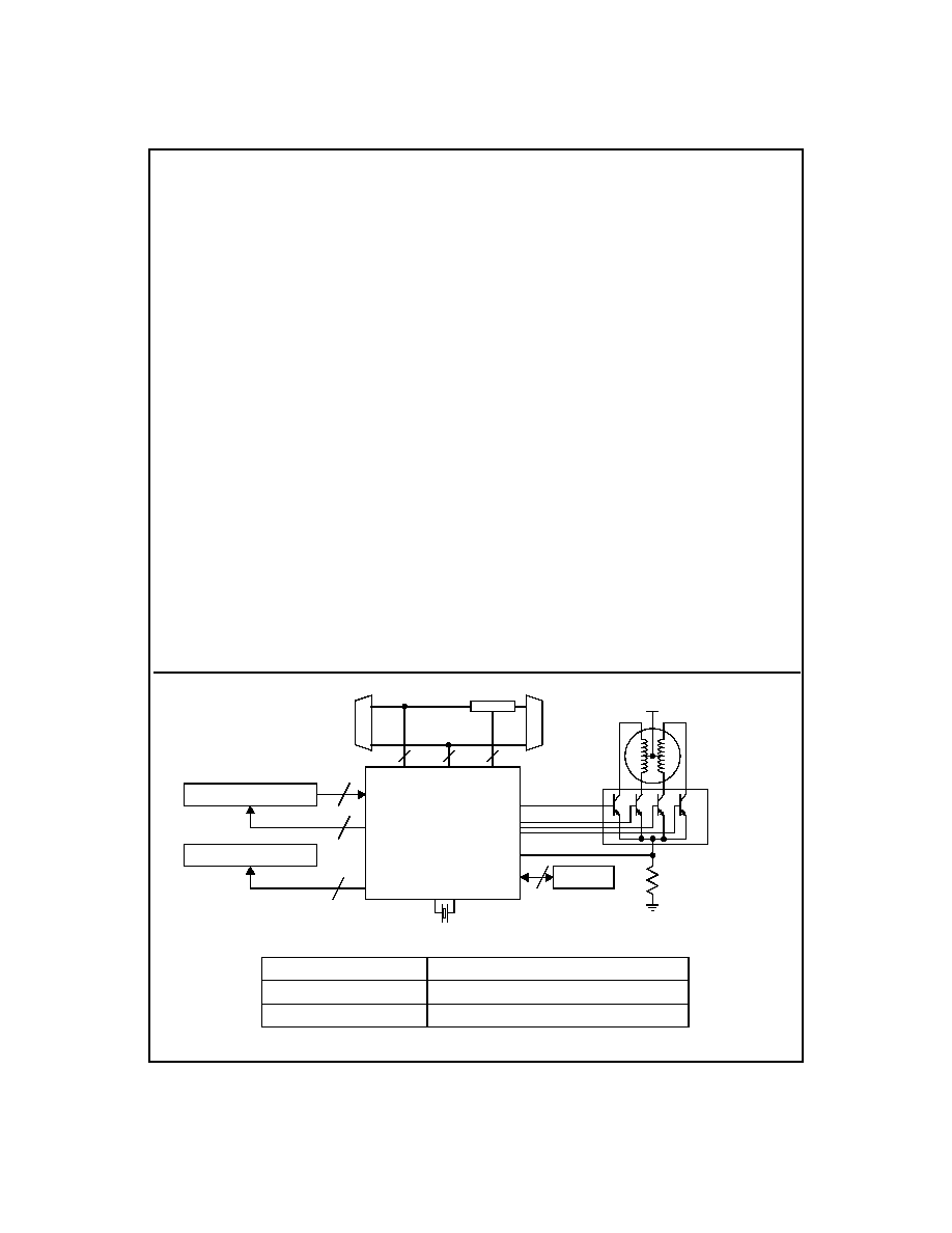
LM9830 36-Bit Color Document Scanner
Scanner Block Diagram
Buffer
To
Computer
To
Printer
DB2
5
DB2
5
CCD/CIS
Illumination
+24V
Stepper
Motor
1-3
1-3
2-6
9
2
8
Power
Transistors
SRAM
28
LM9830VJD
Ordering Information
Commercial (0∞C
T
A
+70∞C)
Package
LM9830VJD
VJD100A 100 Pin Thin Quad Flatpac
LM9830VJDX
VJD100A 100 Pin Thin Quad Flatpac, Tape & Reel
November 1998
LM9830
36-
B
i
t Co
l
o
r Do
c
u
ment
S
cann
e
r
N
©1998 National Semiconductor Corporation
TRI-STATEÆ is a registered trademark of National Semiconductor Corporation.
2
http://www.national.com
Electrical Characteristics
The following specifications apply for AGND=DGND=DGND
I/O
=DGND
SRAM
=0V, V
A
=V
D
=V
DI/O
=V
SRAM
=+5.0V
DC
,
f
CRYSTAL IN
= 50MHz. Boldface limits apply for T
A
=T
J
=T
MIN
to T
MAX
; all other limits T
A
=T
J
=25∞C. (Notes 7, 8, & 12)
Symbol
Parameter
Conditions
Typical
(Note 9)
Limits
(Note 10)
Units
(Limits)
CCD/CIS Source Requirements for Full Specified Accuracy and Dynamic Range (Note 12)
V
OS PEAK
Sensor's Maximum Output Signal
Amplitude before LM9830 Analog Front
End Saturation
Gain = 0.933
Gain = 3.0
Gain = 9.0
2.1
0.65
0.21
V
V
V
Full Channel Characteristics
Resolution with No Missing Codes
12
bits (min)
INL
Integral Non-Linearity Error (Note 11)
-1.1
+4.6
-7
+10
LSB (min)
LSB (max)
DNL
Differential Non-Linearity
-0.5
+0.7
-0.9
+2.0
LSB (min)
LSB (max)
C
Analog Channel Gain Constant
(ADC Codes/V)
Includes voltage reference
variation, gain setting = 1
2048
1863
2129
LSB (min)
LSB (max)
V
OS1
Pre-Boost Analog Channel Offset Error,
CCD Mode
4
-21
+34
mV (min)
mV (max)
V
OS1
Pre-Boost Analog Channel Offset Error,
CIS Mode
12
-15
+38
mV (min)
mV (max)
V
OS2
Pre-PGA Analog Channel Offset Error
-30
-58
+8
mV (min)
mV (max)
V
OS3
Post-PGA Analog Channel Offset Error
-21
-59
+14
mV (min)
mV (max)
Coarse Color Balance PGA Characteristics (Configuration Registers 3B, 3C, and 3D)
Monotonicity
5
bits (min)
G
0
(Minimum PGA Gain)
PGA Setting = 0
0.93
.90
.96
V/V (min)
V/V (max)
G
31
(Maximum PGA Gain)
PGA Setting = 31
3.05
2.98
3.15
V/V (min)
V/V (max)
x3 Boost Gain
x3 Boost Setting On
(bit B5 of Gain Register is set)
2.99
2.86
3.08
V/V (min)
V/V (max)
Gain Error at any gain (Note 13)
±0.2
±1.6
% (max)
Positive Supply Voltage (V
+
=V
A
=V
D
=V
DI/O
=V
SRAM
)
With Respect to
GND=AGND=DGND=DGND
I/O
=DGND
SRAM
6.5V
Voltage On Any Input or Output Pin
-0.3V to V
+
+0.3V
Input Current at any pin (Note 3)
±25mA
Package Input Current (Note 3)
±50mA
Package Dissipation at T
A
= 25∞C
(Note 4)
ESD Susceptibility (Note 5)
Human Body Model
1000V
Soldering Information
Infrared, 10 seconds (Note 6)
235∞C
Storage Temperature
-65∞C to +150∞
Operating Temperature Range
T
MIN
T
A
T
MAX
LM9830VJD
0∞C
T
A
+70∞C
V
A
Supply Voltage
+4.5V to +5.5V
V
D
Supply Voltage
+4.5V to +5.5V
V
DI/O
Supply Voltage
+4.5V to +5.5V
|V
A
-V
D
|, |V
A
-V
DI/O
|, |V
A
-V
SRAM
|, |V
D
-V
DI/O
|,
|V
D
-V
SRAM
|, |V
DI/O
-V
SRAM
|,
100mV
Input Voltage Range
-0.05V to V
+
+ 0.05V
Absolute Maximum Ratings
(Notes 1 & 2)
Operating Ratings
(Notes 1 & 2)
3
http://www.national.com
Static Offset DAC Characteristics (Configuration Registers 38, 39, and 3A)
Monotonicity
6
bits (min)
Offset DAC LSB size
PGA gain = 1
9.3
5.8
12.7
mV (min)
mV (max)
Offset DAC Adjustment Range
PGA gain = 1
±290
±270
mV (min)
Analog Input Characteristics
Average OS
R
, OS
G
, OS
B
Input Current
CDS Enabled, OS = 3.5V
DC
±80
nA
OS
R
, OS
G
, OS
B
Input Current
CDS Disabled, OS = 3.5V
DC
±24
±30
µA (max)
Internal Voltage Reference Characteristics
V
BANDGAP
Voltage Reference Output Voltage
1.2
V
V
REF LO
Negative Reference Output Voltage
V
REF MID
-1.0
V
V
REF MID
Midpoint Reference Output Voltage
V
A
/2.0
V
V
REF HI
Positive Reference Output Voltage
V
REF MID
+1.0
V
DC and Logic Electrical Characteristics
The following specifications apply for AGND=DGND=DGND
I/O
=DGND
SRAM
=0V, V
A
=V
D
=V
DI/O
=V
SRAM
=+5.0V
DC
,
f
CRYSTAL IN
= 50MHz. Boldface limits apply for T
A
=T
J
=T
MIN
to T
MAX
; all other limits T
A
=T
J
=25∞C. (Notes 7 & 8)
Symbol
Parameter
Conditions
Typical
(Note 9)
Limits
(Note 10)
Units
(Limits)
Digital Input Characteristics for DB0-DB7, D0-D7, STROBE, AUTOFEED, INIT, SELECT IN, PSENSE#1, PSENSE#2, MISC I/O
#1, MISC I/O #2, CMODE
V
IN(1)
Logical "1" Input Voltage
V
DI/O
=5.5V
2.0
V (min)
V
IN(0)
Logical "0" Input Voltage
V
DI/O
=4.5V
0.8
V (max)
I
IN
Input Leakage Current
±500
nA
C
IN
Input Capacitance
5
pF
Digital Output Characteristics for DB0-DB7, A0-A17, RD, WR (SRAM Interface)
V
OUT(1)
Logical "1" Output Voltage
V
DI/O
=4.5V, I
OUT
=-4mA
2.4
V (min)
V
OUT(0)
Logical "0" Output Voltage
V
DI/O
=5.5V, I
OUT
=8mA
0.4
V (max)
Digital Output Characteristics for D0-D7, ERROR, ACK, BUSY, PE, SELECT (Parallel Port Interface)
V
OUT(1)
Logical "1" Output Voltage
V
DI/O
=4.5V, I
OUT
=-4mA
2.4
V (min)
V
OUT(0)
Logical "0" Output Voltage
V
DI/O
=5.5V, I
OUT
=14mA
0.4
V (max)
Digital Output Characteristics for MISC I/O #1, MISC I/O #2, A, B, A, B, TR1, TR2, ¯1, ¯2, RS, CP1, CP2, TRISTATE, LATCH,
LAMP
R
, LAMP
G
, LAMP
B
V
OUT(1)
Logical "1" Output Voltage
V
DI/O
=4.5V, I
OUT
=-4mA
2.4
V (min)
V
OUT(0)
Logical "0" Output Voltage
V
DI/O
=5.5V, I
OUT
=8mA
0.4
V (max)
Electrical Characteristics
(Continued)
The following specifications apply for AGND=DGND=DGND
I/O
=DGND
SRAM
=0V, V
A
=V
D
=V
DI/O
=V
SRAM
=+5.0V
DC
,
f
CRYSTAL IN
= 50MHz. Boldface limits apply for T
A
=T
J
=T
MIN
to T
MAX
; all other limits T
A
=T
J
=25∞C. (Notes 7, 8, & 12)
Symbol
Parameter
Conditions
Typical
(Note 9)
Limits
(Note 10)
Units
(Limits)
4
http://www.national.com
CRYSTAL IN, CRYSTAL OUT Characteristics
XTAL
OUT DC
CRYSTAL OUT Bias Level (Offset)
0.8
V
XTAL
OUT AC
CRYSTAL OUT Amplitude
f
CRYSTAL
= 50MHz
0.8
V
P-P
Power Supply Characteristics
I
A
Analog Supply Current
(V
A
pins)
Operating
Standby
64
0.75
83
0.95
mA (max)
mA (max)
I
D I/O
Digital I/O Supply Current
(V
D I/O
, V
D
, and V
SRAM
pins)
Operating
Standby
40
5
48
6.5
mA (max)
mA (max)
AC Electrical Characteristics
The following specifications apply for AGND=DGND=DGND
I/O
=DGND
SRAM
=0V, V
A
=V
D
=V
DI/O
=V
SRAM
=+5.0V
DC
,
f
CRYSTAL IN
= 50MHz, MCLK DIVIDER = 1.0 (unless otherwise noted), f
MCLK
= f
CRYSTAL IN
/MCLK DIVIDER, f
ADC CLK
= f
MCLK
/8,
C
L
(databus loading) = 20pF/pin. Boldface limits apply for T
A
=T
J
=T
MIN
to T
MAX
; all other limits T
A
=T
J
=25∞C. (Notes 7 & 8)
Symbol
Parameter
Conditions
Typical
(Note 9)
Limits
(Note 10)
Units
(Limits)
Parallel Port Address Write (Figure 1)
t
SETUP1
D0-D7 (Address) valid to SELECT IN
falling
-60
-10
ns (min)
t
SETUP2
STROBE falling edge to SELECT IN
falling
-15
-10
ns (min)
t
SI-B1
SELECT IN falling to BUSY rising
25
40
ns (max)
t
B-SI
BUSY rising to SELECT IN rising
0
20
ns (min)
t
HOLD1
SELECT IN rising to STROBE rising
-45
-15
ns (min)
t
SI-B2
SELECT IN rising to BUSY falling
33
50
ns (max)
t
HOLD2
D0-D7 (Address) hold time after
BUSY falling
-10
0
ns (min)
Parallel Port Data Write (Figure 2)
t
SETUP1
D0-D7 valid or STROBE falling to
SELECT IN falling
-60
-10
ns (min)
t
SETUP2
STROBE falling to AUTOFEED falling
-25
-10
ns (min)
t
AF-B1
AUTOFEED falling to BUSY rising
34
50
ns (max)
t
B-AF1
BUSY rising to AUTOFEED rising
0
20
ns (min)
t
HOLD1
AUTOFEED rising to STROBE rising
-40
-10
ns (min)
t
AF-B2
AUTOFEED rising to BUSY falling
All Except Dataport
Dataport
16
1.5 t
ADC CLK
35
3 t
ADC CLK
ns (max)
ns (max)
t
HOLD2
D0-D7 valid after BUSY falling
-10
0
ns (min)
DC and Logic Electrical Characteristics
The following specifications apply for AGND=DGND=DGND
I/O
=DGND
SRAM
=0V, V
A
=V
D
=V
DI/O
=V
SRAM
=+5.0V
DC
,
f
CRYSTAL IN
= 50MHz. Boldface limits apply for T
A
=T
J
=T
MIN
to T
MAX
; all other limits T
A
=T
J
=25∞C. (Notes 7 & 8)
Symbol
Parameter
Conditions
Typical
(Note 9)
Limits
(Note 10)
Units
(Limits)

5
http://www.national.com
Parallel Port 8 Bit Data Read (Figure 3)
t
AF-B3
AUTOFEED falling to BUSY rising
All Except Dataport
Dataport
25
1.5 t
ADC CLK
45
3 t
ADC CLK
ns (max)
ns (max)
t
EPP ACCESS
D0-D7 valid before BUSY rising
(Note 14)
7
-5
ns (min)
t
B-AF2
BUSY rising to AUTOFEED rising
1
10
ns (min)
t
EPP HOLD
AUTOFEED rising to D0-D7 Tri-State
20
10
27
ns (min)
ns (max)
t
AF-B4
AUTOFEED rising to BUSY falling
3 t
MCLK
4 t
MCLK
ns (max)
Nibble Data Read (Figure 4)
t
AF-B3
AUTOFEED falling to BUSY rising
All Except Dataport
Dataport
25
1.5 t
ADC CLK
45
3 t
ADC CLK
ns (max)
ns (max)
t
NIB ACCESS1
D4-D7 valid before BUSY rising
2
-20
ns (min)
t
B-AF2
BUSY rising to AUTOFEED rising
1
10
ns (min)
t
NIB ACCESS2
D0-D3 valid after AUTOFEED rising
5
15
ns (max)
t
AF-B4
AUTOFEED rising edge to BUSY
falling
3 t
MCLK
4 t
MCLK
ns (max)
Microprocessor Mode (Figures 5, 6, and 7)
t
ALE SETUP
D0-D7 (Address) valid before ALE
falling
0
6
ns (min)
t
ALE HOLD
D0-D7 (Address) valid after ALE
falling
2
8
ns (min)
t
ALE
ALE high time
2
8
ns (min)
t
ALE-R/W
ALE falling to CS/RD/WR falling (next
operation)
16
ns (min)
t
WR SETUP
D0-D7 valid before WR rising
0
6
ns (min)
t
WR HOLD
D0-D7 valid after WR rising
2
10
ns (min)
t
WR
WR pulse width
3
10
ns (min)
t
RD ACCESS
RD low to D0-D7 valid
22
31
ns (max)
t
RD TRI-STATE
RD high to D0-D7 Tri-State
20
28
ns (max)
AC Electrical Characteristics
The following specifications apply for AGND=DGND=DGND
I/O
=DGND
SRAM
=0V, V
A
=V
D
=V
DI/O
=V
SRAM
=+5.0V
DC
,
f
CRYSTAL IN
= 50MHz, MCLK DIVIDER = 1.0 (unless otherwise noted), f
MCLK
= f
CRYSTAL IN
/MCLK DIVIDER, f
ADC CLK
= f
MCLK
/8,
C
L
(databus loading) = 20pF/pin. Boldface limits apply for T
A
=T
J
=T
MIN
to T
MAX
; all other limits T
A
=T
J
=25∞C. (Notes 7 & 8)
Symbol
Parameter
Conditions
Typical
(Note 9)
Limits
(Note 10)
Units
(Limits)