 | ÐлекÑÑоннÑй компоненÑ: LMV791 | СкаÑаÑÑ:  PDF PDF  ZIP ZIP |
Äîêóìåíòàöèÿ è îïèñàíèÿ www.docs.chipfind.ru
LMV791
17 MHz, Low Noise, CMOS Input, 1.8V Operational
Amplifier
General Description
The LMV791 low noise, CMOS input operational amplifier
offers a low input voltage noise density of 5.8 nV/
while
consuming only 1.15 mA of quiescent current. The LMV791
is a unity gain stable op amp and has a gain bandwidth of 17
MHz. The LMV791 has a supply voltage range of 1.8V to
5.5V and can operate from a single supply. The LMV791
features a rail-to-rail output stage capable of driving a 600
load and sourcing as much as 60 mA of current.
The LMV791 provides optimal performance in low voltage
and low noise systems. A CMOS input stage, with typical
input bias currents in the range of a few femtoAmperes, and
an input common mode voltage range which includes
ground make the LMV791 ideal for low power sensor appli-
cations. The LMV791 has a built-in enable feature which can
be used to optimize power dissipation in low power applica-
tions.
The LMV791 is manufactured using National's advanced
VIP50 process and is available in a 6-pin TSOT23 package.
Features
(Typical 5V supply, unless otherwise noted)
n
Input referred voltage noise
5.8 nV/
n
Input bias current
0.1 pA
n
Unity gain bandwidth
17 MHz
n
Supply current
1.15 mA
n
Guaranteed 2.5V and 5.0V performance
n
Rail-to-rail output swing
--
@
10 k
load
25 mV from rail
--
@
2 k
load
35 mV from rail
n
Total harmonic distortion
0.01%
@
1 kHz, 600
n
Temperature range
-40
o
C to 125
o
C
Applications
n
Photodiode Amplifiers
n
Active filters and buffers
n
Low noise signal processing
n
Medical Instrumentation
n
Sensor interface applications
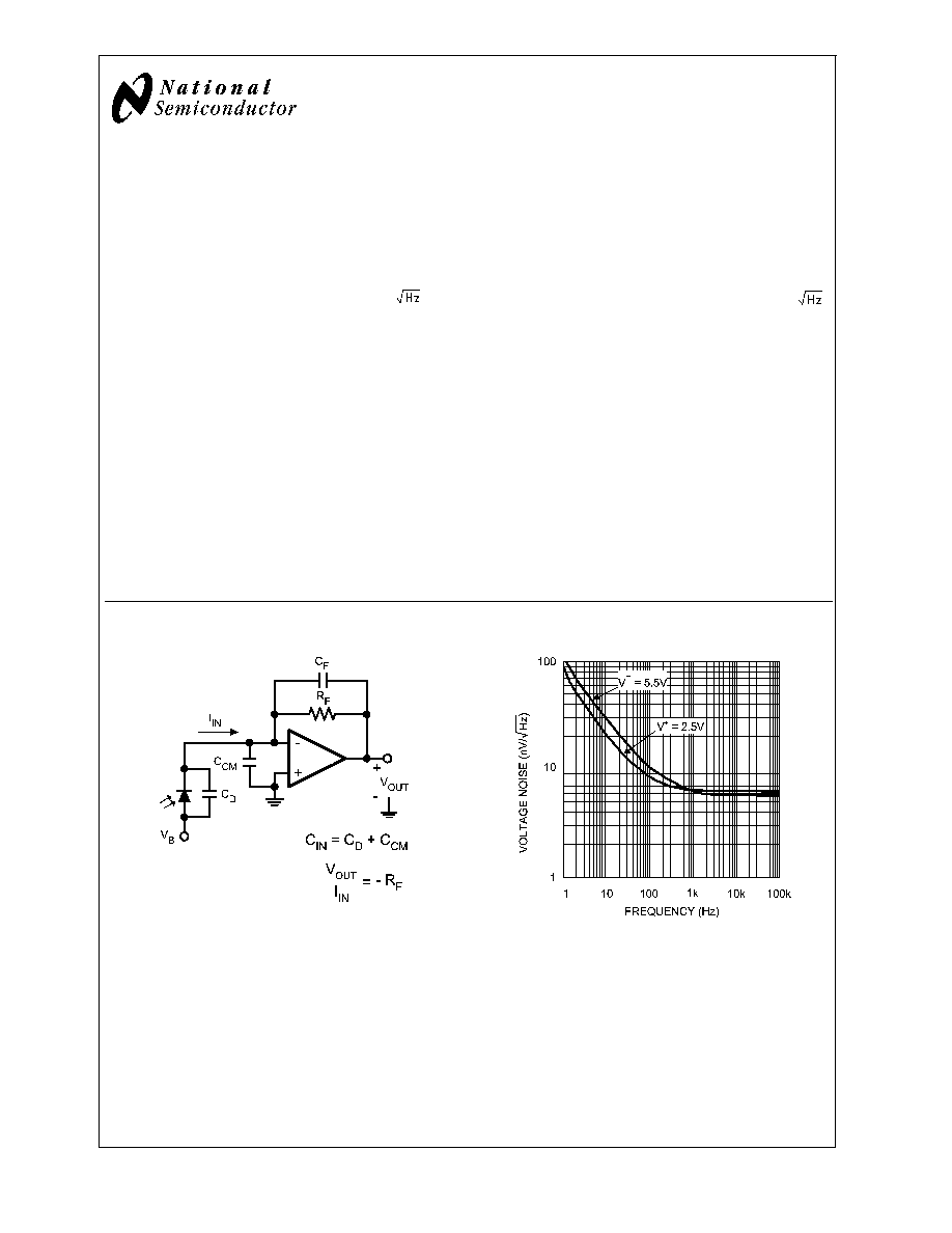
Typical Application
20116869
Photodiode Transimpedance Amplifier
20116839
Input Referred Voltage Noise vs. Frequency
September 2005
LMV791
17
MHz,
Low
Noise,
CMOS
Input,
1.8V
Operational
Amplifier
© 2005 National Semiconductor Corporation
DS201168
www.national.com
Absolute Maximum Ratings
(Note 1)
If Military/Aerospace specified devices are required,
please contact the National Semiconductor Sales Office/
Distributors for availability and specifications.
ESD Tolerance (Note 2)
Human Body
±
2000V
Machine Model
±
200V
V
IN
Differential
0.3V
Supply Voltage (V
+
V
-
)
6.0V
Input/Output Pin Voltage
V
+
+0.3V, V
-
-0.3V
Storage Temperature Range
-65°C to 150°C
Junction Temperature (Note 3)
+150°C
Soldering Information
Infrared or Convection (20 sec)
235°C
Wave Soldering Lead Temp (10
sec)
260°C
Operating Ratings
(Note 1)
Temperature Range (Note 3)
-40°C to 125°C
Supply Voltage (V
+
V
-
)
-40°C
T
A
125°C
2V to 5.5V
0°C
T
A
125°C
1.8V to 5.5V
Package Thermal Resistance (
JA
(Note 3))
6-Pin TSOT23
170°C/W
2.5V Electrical Characteristics
Unless otherwise specified, all limits are guaranteed for T
A
= 25°C, V
+
= 2.5V, V
-
= 0V, V
CM
= V
+
/2, V
EN
= V
+
. Boldface limits
apply at the temperature extremes.
Symbol
Parameter
Conditions
Min
(Note 5)
Typ
(Note 4)
Max
(Note 5)
Units
V
OS
Input Offset Voltage
0.1
±
1.35
±
1.65
mV
TC V
OS
Input Offset Average Drift
(Note 6)
1.0
µV/°C
I
B
Input Bias Current
V
CM
= 1.0V
(Notes 7, 8)
0.05
0.5
50
pA
I
OS
Input Offset Current
(Note 8)
10
fA
CMRR
Common Mode Rejection
Ratio
0V
V
CM
1.4V
80
75
94
dB
PSRR
Power Supply Rejection
Ratio
2V
V
+
5.5V, V
CM
= 0V
80
75
100
dB
1.8V
V
+
5.5V, V
CM
= 0V
80
98
CMVR
Input Common-Mode Voltage
Range
CMRR
60 dB
CMRR
55 dB
-0.3
-0.3
1.5
1.5
V
A
VOL
Large Signal Voltage Gain
V
OUT
= 0.15V to 2.2V,
R
LOAD
= 2 k
to V
+
/2
85
80
98
dB
V
OUT
= 0.15V to 2.2V,
R
LOAD
= 10 k
to V
+
/2
88
84
110
V
OUT
Output Swing High
R
LOAD
= 2 k
to V
+
/2
75
82
25
mV from
rail
R
LOAD
= 10 k
to V
+
/2
65
71
20
Output Swing Low
R
LOAD
= 2 k
to V
+
/2
30
75
78
R
LOAD
= 10 k
to V
+
/2
15
65
67
I
OUT
Output Short Circuit Current
Sourcing to V
-
V
IN
= 200 mV (Note 9)
35
28
47
mA
Sinking to V
+
V
IN
= 200 mV (Note 9)
7
5
15
I
S
Supply Current per Amplifier
Enable Mode V
EN
>
2.1
0.95
1.30
1.65
mA
Shutdown Mode V
EN
<
0.4
0.02
1
5
µA
LMV791
www.national.com
2
2.5V Electrical Characteristics
(Continued)
SR
Slew Rate
A
V
= +1, Rising (10% to 90%)
8.5
V/µs
A
V
= +1, Falling (90% to 10%)
10.5
GBWP
Gain Bandwidth Product
14
MHz
e
n
Input-Referred Voltage Noise
f = 1 kHz
6.2
nV/
i
n
Input-Referred Current Noise
f = 1 kHz
0.01
pA/
t
on
Turn-on Time
140
ns
t
off
Turn-off Time
1000
ns
V
EN
Enable Pin Voltage Range
Enable Mode
2.1 to 2.5
2 to 2.5
V
Shutdown Mode
0 to 0.4
0 to 0.5
I
EN
Enable Pin Input Current
Enable Mode V
EN
>
2.1V (Note 7)
1.5
3
µA
Shutdown Mode V
EN
<
0.4V (Note 7)
0.003
0.1
THD+N
Total Harmonic Distortion +
Noise
f = 1 kHz, A
V
= 1, R
LOAD
= 600
0.01
%
5V Electrical Characteristics
Unless otherwise specified, all limits guaranteed for T
A
= 25°C, V
+
= 5V, V
-
= 0V, V
CM
= V
+
/2, V
EN
= V
+
. Boldface limits apply
at the temperature extremes.
Symbol
Parameter
Conditions
Min
(Note 5)
Typ
(Note 4)
Max
(Note 5)
Units
V
OS
Input Offset Voltage
0.1
±
1.35
±
1.65
mV
TC V
OS
Input Offset Average Drift
(Note 6)
1.0
µV/°C
I
B
Input Bias Current
V
CM
= 2.0V
(Notes 7, 8)
0.1
1
100
pA
I
OS
Input Offset Current
(Note 8)
10
fA
CMRR
Common Mode Rejection
Ratio
0V
V
CM
3.7V
80
75
100
dB
PSRR
Power Supply Rejection
Ratio
2V
V
+
5.5V, V
CM
= 0V
80
75
100
dB
1.8V
V
+
5.5V, V
CM
= 0V
80
98
CMVR
Input Common-Mode Voltage
Range
CMRR
60 dB
CMRR
55 dB
-0.3
-0.3
4
4
V
A
VOL
Large Signal Voltage Gain
V
OUT
= 0.3V to 4.7V,
R
LOAD
= 2 k
to V
+
/2
85
80
97
dB
V
OUT
= 0.3V to 4.7V,
R
LOAD
= 10 k
to V
+
/2
88
84
110
V
OUT
Output Swing High
R
LOAD
= 2 k
to V
+
/2
75
82
35
mV from
rail
R
LOAD
= 10 k
to V
+
/2
65
71
25
Output Swing Low
R
LOAD
= 2 k
to V
+
/2
50
75
78
R
LOAD
= 10 k
to V
+
/2
20
65
67
I
OUT
Output Short Circuit Current
Sourcing to V
-
V
IN
= 200 mV (Note 9)
45
37
60
mA
Sinking to V
+
V
IN
= 200 mV (Note 9)
10
6
21
I
S
Supply Current per Amplifier
Enable Mode (V
EN
>
4.6 V)
1.15
1.40
1.75
mA
Shutdown Mode (V
EN
<
0.4V)
0.14
1
5
µA
LMV791
www.national.com
3
5V Electrical Characteristics
(Continued)
SR
Slew Rate
A
V
= +1, Rising (10% to 90%)
6.0
9.5
V/µs
A
V
= +1, Falling (90% to 10%)
7.5
11.5
GBWP
Gain Bandwidth Product
17
MHz
e
n
Input - Referred Voltage
Noise
f = 1 kHz
5.8
nV/
i
n
Input-Referred Current Noise
f = 1 kHz
0.01
pA/
t
on
Turn-on Time
110
ns
t
off
Turn-off Time
800
ns
V
EN
Enable Pin Voltage Range
Enable Mode
4.6 to 5
4.5 to 5
V
Shutdown Mode
0 to 0.4
0 to 0.5
I
EN
Enable Pin Input Current
Enable Mode V
EN
>
4.6V
(Note 7)
5.6
10
µA
Shutdown Mode V
EN
<
0.4V
(Note 7)
0.005
0.2
THD+N
Total Harmonic Distortion +
Noise
f = 1 kHz, A
V
= 1, R
LOAD
= 600
0.01
%
Note 1: Absolute Maximum Ratings indicate limits beyond which damage to the device may occur. Operating Ratings indicate conditions for which the device is
intended to be functional, but specific performance is not guaranteed. For guaranteed specifications and the test conditions, see the Electrical Characteristics Tables.
Note 2: Human Body Model: 1.5 k
in series with 100 pF. Machine Model: 0 in series with 200 pF
Note 3: The maximum power dissipation is a function of T
J(MAX)
,
JA
. The maximum allowable power dissipation at any ambient temperature is
P
D
= (T
J(MAX)
- T
A
)/
JA
. All numbers apply for packages soldered directly onto a PC Board.
Note 4: Typical values represent the parametric norm at the time of characterization.
Note 5: Limits are 100% production tested at 25°C. Limits over the operating temperature range are guaranteed through correlations using the statistical quality
control (SQC) method.
Note 6: Offset voltage average drift is determined by dividing the change in V
OS
by temperature change.
Note 7: Positive current corresponds to current flowing into the device.
Note 8: Input bias current and input offset current are guaranteed by design
Note 9: The short circuit test is a momentary test, the short circuit duration is 1.5 ms.
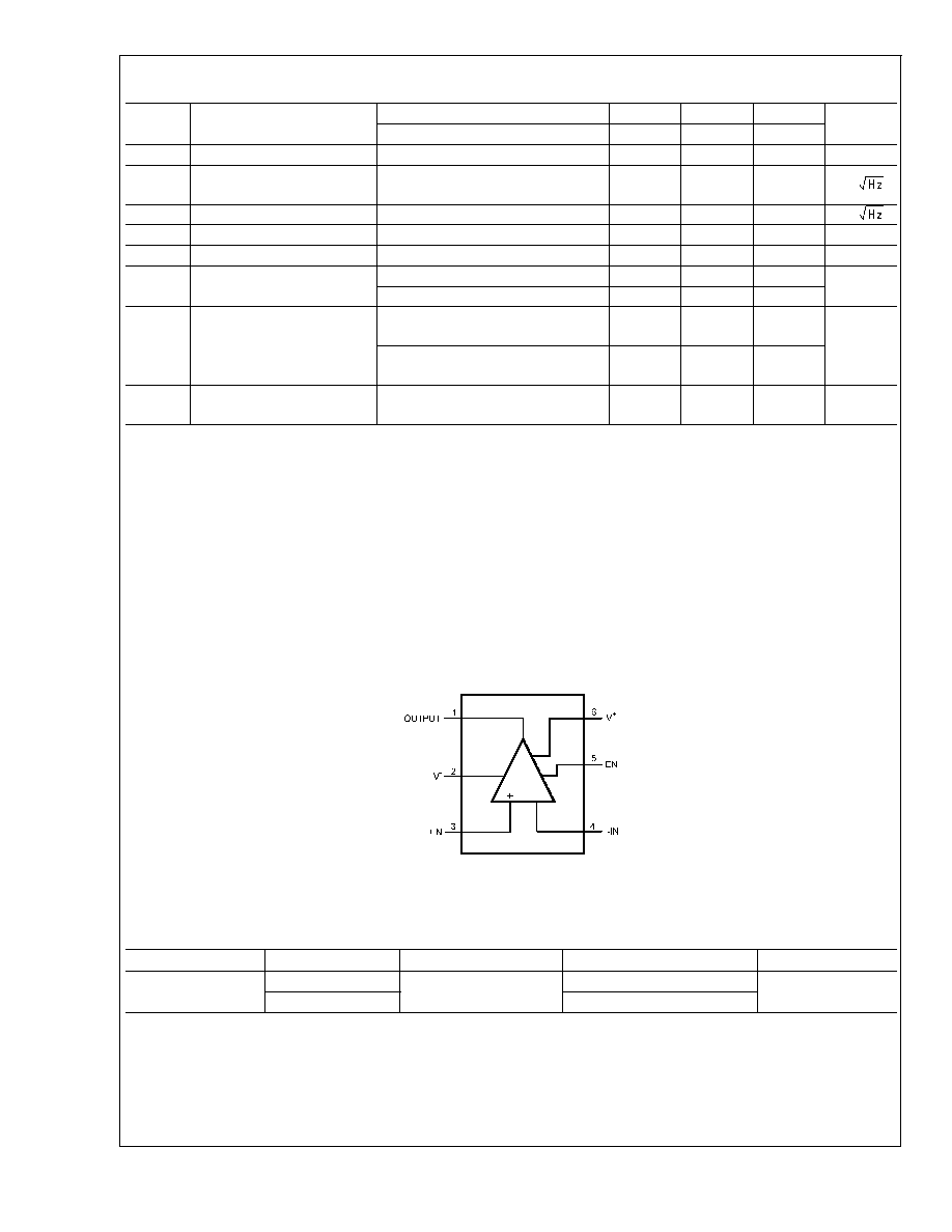
Connection Diagram
6-Pin TSOT23
20116801
Top View
Ordering Information
Package
Part Number
Package Marking
Transport Media
NSC Drawing
6-Pin TSOT23
LMV791MK
AS1A
1k Units Tape and Reel
MK06A
LMV791MKX
3k Units Tape and Reel
LMV791
www.national.com
4
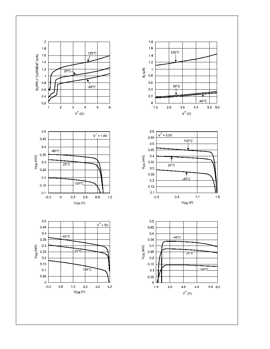
Typical Performance Characteristics
Unless otherwise specified, T
A
= 25°C, V
=0, V
+
= Supply
Voltage = 5V, V
CM
= V
+
/2, V
EN
= V
+
Supply Current vs. Supply Voltage
Supply Current vs. Supply Voltage in Shutdown Mode
20116805
20116806
V
OS
vs. V
CM
V
OS
vs. V
CM
20116809
20116851
V
OS
vs. V
CM
V
OS
vs. Supply Voltage
20116811
20116812
LMV791
www.national.com
5
Document Outline