LMX2335U/LMX2336U
PLLatinum
TM
Ultra Low Power Dual Frequency
Synthesizer for RF Personal Communications
LMX2335U
1.2 GHz/1.2 GHz
LMX2336U
2.0 GHz/1.2 GHz
General Description
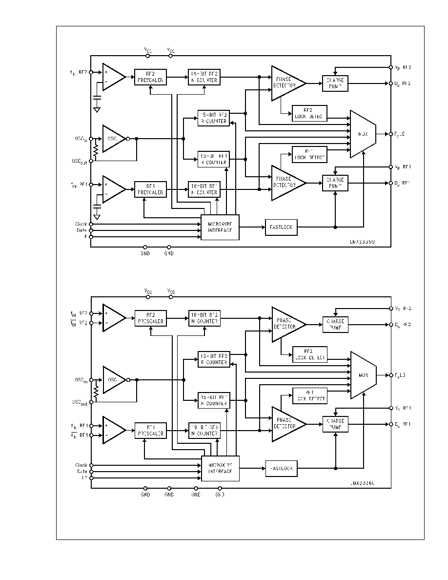
The LMX2335U and LMX2336U devices are high perfor-
mance frequency synthesizers with integrated dual modulus
prescalers. The LMX2335U and LMX2336U devices are
designed
for
use
in
applications
requiring
two
RF
phase-locked loops.
A 64/65 or a 128/129 prescale ratio can be selected for each
RF synthesizer. Using a proprietary digital phase locked loop
technique, the LMX2335U and LMX2336U devices generate
very stable, low noise control signals for the RF voltage
controlled oscillators. Both RF synthesizers include a
two-level programmable charge pump. The RF1 synthesizer
has dedicated Fastlock circuitry.
Serial data is transferred to the devices via a three wire
interface (Data, LE, Clock). Supply voltages from 2.7V to
5.5V are supported. The LMX2335U and the LMX2336U
feature very low current consumption:
LMX2335U (1.2 GHz)≠ 3.0 mA, LMX2336U (2.0 GHz)≠
3.5 mA at 3.0V.
The LMX2335U device is available in 16-pin TSSOP, and
16-pin Chip Scale Package (CSP) surface mount plastic
packages. The LMX2336U device is available in 20-Pin
TSSOP, 24-Pin CSP, and 20-Pin UTCSP surface mount
plastic packages.
Features
n
Ultra Low Current Consumption
n
Upgrade and Compatible to the LMX2335L and
LMX2336L devices
n
2.7V to 5.5V operation
n
Selectable Synchronous or Asynchronous Powerdown
Mode:
I
CC-PWDN
= 1 µA typical at 3.0V
n
Selectable Dual Modulus Prescaler
RF1: 64/65 or 128/129
RF2: 64/65 or 128/129
n
Selectable Charge Pump TRI-STATE
Æ
Mode
n
Programmable Charge Pump Current Levels
RF1 and RF2: 0.95 or 3.8 mA
n
Selectable Fastlock
TM
Mode for the RF1 Synthesizer
n
Push-Pull Analog Lock Detect Mode
n
LMX2335U is available in 16-Pin TSSOP and 16-Pin
CSP
n
LMX2336U is available in 20-Pin TSSOP, 24-Pin CSP,
and 20-Pin UTCSP
Applications
n
Mobile Handsets
(GSM, GPRS, W-CDMA, CDMA, PCS, AMPS, PDC,
DCS)
n
Cordless Handsets (DECT, DCT)
n
Wireless Data
n
Cable TV Tuners
Thin Shrink Small Outline Package (MTC16)
Thin Shrink Small Outline Package (MTC20)
10136787
10136780
Chip Scale Package (SLB16A)
Chip Scale Package (SLB24A)
Ultra Thin Chip Scale Package
(SLE20A)
10136788
10136781
10136795
TRI-STATE
Æ
is a registered trademark of National Semiconductor Corporation.
Fastlock
TM
, MICROWIRE
TM
and PLLatinum
TM
are trademarks of National Semiconductor Corporation.
November 2002
LMX2335U/LMX2336U
PLLatinum
Ultra
Low
Power
Dual
Frequency
Synthesizer
for
RF
Personal
Communications
© 2002 National Semiconductor Corporation
DS101367
www.national.com
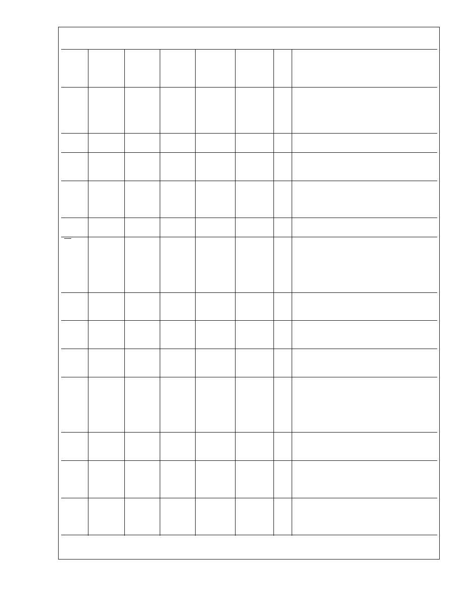
Pin Descriptions
Pin
Name
Pin No.
LMX2336U
20-Pin
UTCSP
Pin No.
LMX2336U
20-Pin
TSSOP
Pin No.
LMX2336U
24-Pin
CSP
Pin No.
LMX2335U
16-Pin
TSSOP
Pin No.
LMX2335U
16-Pin
CSP
I/O
Description
V
CC
20
1
24
1
16
≠
Power supply bias for the RF1 PLL analog and
digital circuits. V
CC
may range from 2.7V to
5.5V. Bypass capacitors should be placed as
close as possible to this pin and be connected
directly to the ground plane.
V
P
RF1
1
2
2
2
1
≠
RF1 PLL charge pump power supply. Must be
V
CC
.
D
o
RF1
2
3
3
3
2
O
RF1 PLL charge pump output. The output is
connected to the external loop filter, which drives
the input of the VCO.
GND
3
4
4
4
3
≠
LMX2335U: Ground for the RF1 PLL analog and
digital circuits.
LMX2336U: Ground for the RF1 PLL digital
circuitry.
f
IN
RF1
4
5
5
5
4
I
RF1 PLL prescaler input. Small signal input from
the VCO.
f
IN
RF1
5
6
6
X
X
I
LMX2335U: Don't care.
LMX2336U: RF1 PLL prescaler complementary
input. For single ended operation, this pin should
be AC grounded. The LMX2336U RF1 PLL can
be driven differentially when the bypass
capacitor is omitted.
GND
6
7
7
X
X
≠
LMX2335U: Don't care.
LMX2336U: Ground for the RF1 PLL analog
circuitry.
OSC
in
7
8
8
6
5
I
Oscillator input. It has an approximate V
CC
/2
input threshold and can be driven from an
external CMOS or TTL logic gate.
OSC
out
8
9
10
7
6
O
Oscillator output. This output is connected
directly to a crystal. If a TCXO is used, it is left
open.
F
o
LD
9
10
11
8
7
O
Programmable multiplexed output pin. Functions
as a general purpose CMOS TRI-STATE output,
RF1/RF2 PLL push-pull analog lock detect
output, N and R divider output, or Fastlock
output, which connects a parallel resistor to the
external loop filter.
Clock
10
11
12
9
8
I
MICROWIRE Clock input. High impedance
CMOS input. Data is clocked into the 22-bit shift
register on the rising edge of Clock.
Data
11
12
14
10
9
I
MICROWIRE Data input. High impedance
CMOS input. Binary serial data. The MSB of
Data is entered first. The last two bits are the
control bits.
LE
12
13
15
11
10
I
MICROWIRE Latch Enable input. High
impedance CMOS input. When LE transitions
HIGH, Data stored in the shift registers is loaded
into one of 4 internal control registers.
LMX2335U/LMX2336U
www.national.com
4

Pin Descriptions
(Continued)
Pin
Name
Pin No.
LMX2336U
20-Pin
UTCSP
Pin No.
LMX2336U
20-Pin
TSSOP
Pin No.
LMX2336U
24-Pin
CSP
Pin No.
LMX2335U
16-Pin
TSSOP
Pin No.
LMX2335U
16-Pin
CSP
I/O
Description
GND
13
14
16
X
X
≠
LMX2335U: Don't care.
LMX2336U: Ground for the RF2 PLL analog
circuitry.
f
IN
RF2
14
15
17
X
X
I
LMX2335U: Don't care.
LMX2336U: RF2 PLL prescaler complementary
input. For single ended operation, this pin should
be AC grounded. The LMX2336U RF2 PLL can
be driven differentially when the bypass
capacitor is omitted.
f
IN
RF2
15
16
18
12
11
I
RF2 PLL prescaler input. Small signal input from
the VCO.
GND
16
17
19
13
12
-
LMX2335U: Ground for the RF2 PLL analog and
digital circuits, MICROWIRE, F
o
LD and oscillator
circuits. LMX2336U: Ground for the RF2 PLL
digital circuitry, MICROWIRE, F
o
LD and
oscillator circuits.
D
o
RF2
17
18
20
14
13
O
RF2 PLL charge pump output. The output is
connected to the external loop filter, which drives
the input of the VCO.
V
P
RF2
18
19
22
15
14
≠
RF2 PLL charge pump power supply. Must be
V
CC
.
V
CC
19
20
23
16
15
≠
Power supply bias for the RF2 PLL analog and
digital circuits, MICROWIRE, F
o
LD and oscillator
circuits. V
CC
may range from 2.7V to 5.5V.
Bypass capacitors should be placed as close as
possible to this pin and be connected directly to
the ground plane.
NC
X
X
1, 9, 13,
21
X
X
≠
LMX2335U: Don't Care.
LMX2336U: No connect.
LMX2335U/LMX2336U
www.national.com
5