 | –≠–ª–µ–∫—Ç—Ä–æ–Ω–Ω—ã–π –∫–æ–º–ø–æ–Ω–µ–Ω—Ç: LMX3305 | –°–∫–∞—á–∞—Ç—å:  PDF PDF  ZIP ZIP |

LMX3305
Triple Phase Locked Loop for RF Personal
Communications
General Description
The LMX3305 contains three Phase Locked Loops (PLL) on
a single chip. It has a RF PLL, an IF Rx PLL and an IF Tx
PLL for CDMA applications. The RF fractional-N PLL uses a
16/17/20/21 quadruple modulus prescaler for PCS applica-
tion and a 8/9/12/13 quadruple modulus prescaler for cellular
application.
Both
quadruple
modulus
prescalers
offer
modulo 1 through 16 fractional compensation circuitry. The
RF fractional-N PLL can be programmed to operate from 800
MHz to 1400MHz in cellular band and 1200MHz to 2300
MHz in PCS band. The IF Rx PLL and the IF Tx PLL are
integer-N frequency synthesizers that operate from 45 MHz
to 600 MHz with 8/9 dual modulus prescalers. Serial data is
transferred into the LMX3305 via a microwire interface
(Clock, Data, & LE).
The RF PLL provides a fastlock feature allowing the loop
bandwidth to be increased by 3X during initial lock-on.
The supply voltage of the LMX3305 ranges from 2.7V to
3.6V. It typically consumes 9 mA of supply current and is
packaged in a 24-pin CSP package.
Features
n
Three PLLs integrated on a single chip
n
RF PLL fractional-N counter
n
16/17/20/21 RF quadruple modulus prescaler for PCS
application
n
8/9/12/13 RF quadruple modulus prescaler for cellular
application
n
2.7V to 3.6V operation
n
Low current consumption: I
CC
= 9 mA (typ) at 3.0V
n
Programmable or logical power down mode: I
CC
=
10 µA (typ) at 3.0V
n
RF PLL Fastlock feature with timeout counter
n
Digital lock detect
n
Microwire Interface with data preset
n
24-pin CSP package
Applications
n
CDMA Cellular telephone systems
Block Diagram
TRI-STATE
Æ
is a registered trademark of National Semiconductor Corporation.
DS101361-1
PRELIMINARY
August 2000
LMX3305
T
riple
Phase
Locked
Loop
for
RF
Personal
Communications
© 2000 National Semiconductor Corporation
DS101361
www.national.com
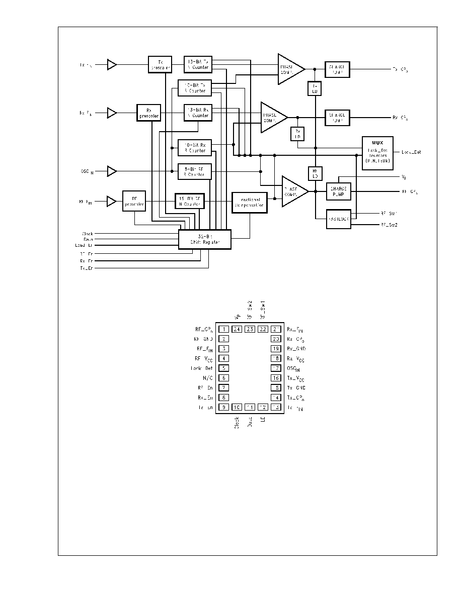
Functional Block Diagram
Connection Diagram
DS101361-2
DS101361-3
Top View
Order Number LMX3305SLBX
See NS Package Number SLB24A
LMX3305
www.national.com
2
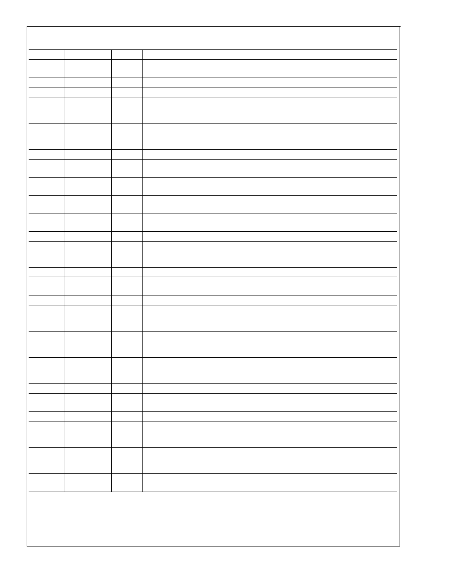
Pin Descriptions
Pin No.
Pin Name
I/O
Description
1
RF_CP
o
O
Charge pump output for RF PLL. For connection to a loop filter for driving the input of
an external VCO.
2
RF_GND
PWR
RF PLL ground.
3
RF_F
IN
I
RF prescaler input. Small signal input from the RF Cellular or PCS VCO.
4
RF_V
CC
PWR
RF PLL power supply voltage. Input may range from 2.7V to 3.6V. Bypass capacitors
should be placed as close as possible to this pin and be connected directly to the
ground plane. Tx V
CC
= Rx V
CC
= RF V
CC
.
5
Lock_Det
O
Multiplexed output of the RF, Rx, and Tx PLL's analog or digital lock detects. The
outputs from the R, N and Fastlock counters can also be selected for test purposes.
Refer to Section 2.3.4 for more detail.
6
N/C
No Connect.
7
RF_En
I
RF PLL enable pin. A LOW on RF En powers down the RF PLL and TRI-STATE
Æ
s the
RF PLL charge pump.
8
Rx_En
I
Rx PLL enable pin. A LOW on Rx En powers down the Rx PLL and TRI-STATEs the
Rx PLL charge pump.
9
Tx_En
I
Tx PLL enable pin. A LOW on Tx En powers down the Tx PLL and TRI-STATEs the
Tx PLL charge pump.
10
Clock
I
High impedance CMOS clock input. Data for the various counters is clocked on the
rising edge into the CMOS input.
11
Data
I
Binary serial data input. Data entered MSB first.
12
LE
I
High impedance CMOS input. When LE goes LOW, data is transferred into the shift
registers. When LE goes HIGH, data is transferred from the internal registers into the
appropriate latches.
13
Tx_F
IN
I
Tx prescaler input. Small signal input from the Tx VCO.
14
Tx_CP
o
O
Charge pump output for Tx PLL. For connection to a loop filter for driving the input of
an external VCO.
15
Tx_GND
Tx PLL ground.
16
Tx_V
CC
PWR
Tx PLL power supply voltage input. Input may range from 2.7V to 3.6V. Bypass
capacitors should be placed as close as possible to this pin and be connected directly
to the ground plane. Tx V
CC
= Rx V
CC
= RF V
CC
.
17
OSC
IN
I
PLL reference input which has a V
CC
/2 input threshold and can be driven from an
external CMOS or TLL logic gate. The R counter is clocked on the falling edge of the
OSC
IN
signal.
18
Rx_V
CC
PWR
Rx PLL power supply voltage. Input ranges from 2.7V to 3.6V. Bypass capacitors
should be placed as close as possible to this pin and be connected directly to the
ground plane. Tx V
CC
= Rx V
CC
= RF V
CC
.
19
Rx_GND
PWR
Rx PLL ground.
20
Rx_CP
o
O
Charge pump output for Rx PLL. For connection to a loop filter for driving the input of
an external VCO.
21
Rx_F
IN
I
Rx prescaler input. Small signal input from the Rx VCO.
22
RF_Sw1
O
An open drain NMOS output which can be use for bandswitching or Fastlocking the
RF PLL. (During Fastlock mode a second loop filter damping resistor can be switched
in parallel with the first to ground.) Refer to Section 2.5.3 for more detail.
23
RF_Sw2
O
An open drain NMOS output which can be use for bandswitching or Fastlocking the
RF PLL. (During Fastlock mode a second loop filter damping resistor can be switched
in parallel with the first to ground.) Refer to Section 2.5.3 for more detail.
24
V
P
O
RF PLL charge pump power supply. An internal voltage doubler can be enabled in 3V
applications to allow the RF charge pump to operate over a wider tuning range.
LMX3305
www.national.com
3
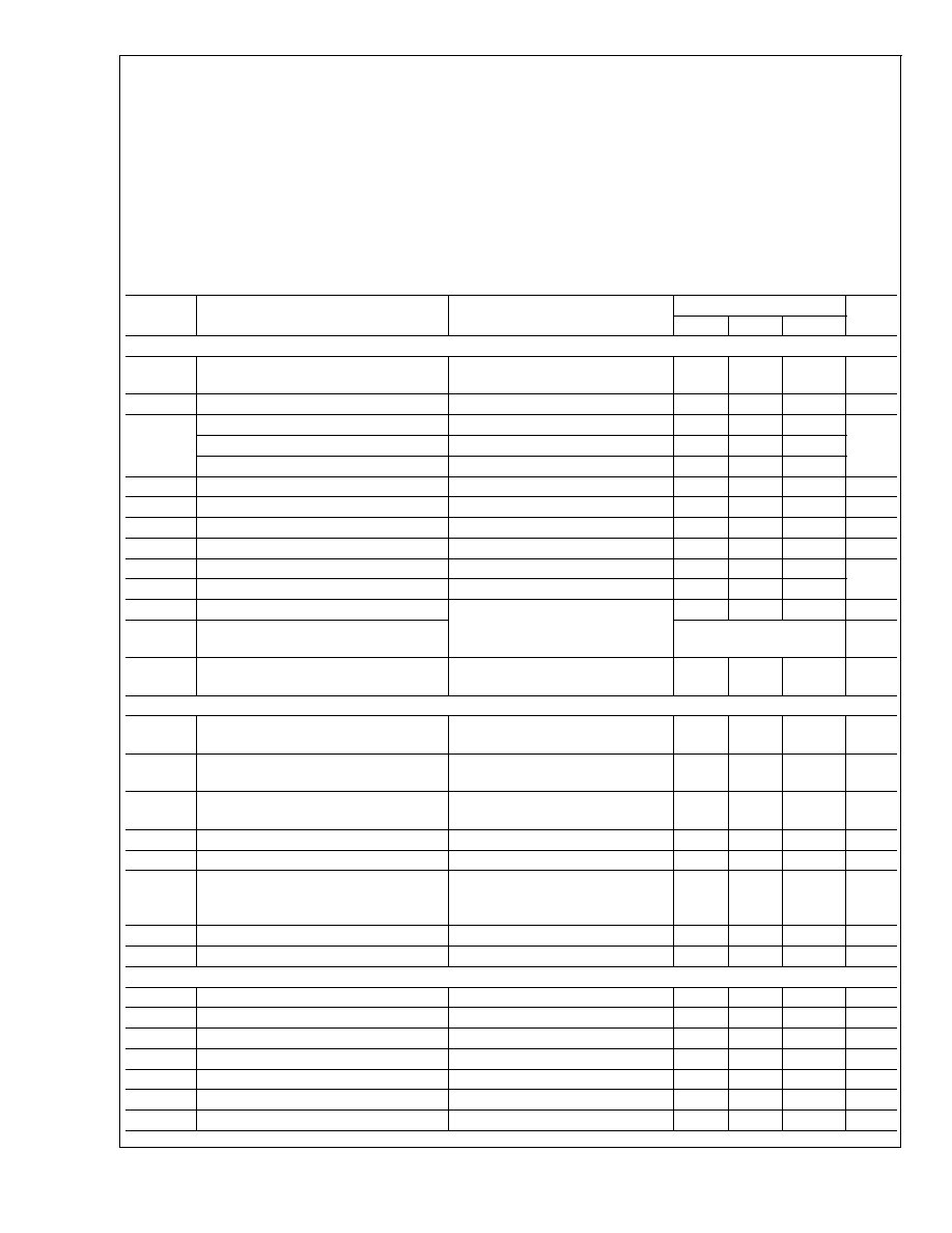
Absolute Maximum Ratings
(Notes 1, 2)
Power Supply Voltage (PLL V
CC
)
(Note 3)
-0.3V to +6.5V
Supply Voltage (V
P
)
-0.3V to +6.5V
Voltage on any Pin with
GND = 0V (V
I
)
-0.3V to V
CC
+0.3V
Storage Temperature Range (T
S
)
-65∞C to +150∞C
Lead Temp. (solder, 4 sec.) (T
L
)
+240∞C
ESD - Whole Body Model (Note 2)
2 kV
Recommended Operating
Conditions
(Note 1)
Power Supply Voltage (PLL V
CC
)
(Note 3)
2.7V to 3.6V
Supply Voltage (V
P
) (Note 3)
PLL V
CC
to 5.5V
Operating Temperature (T
A
)
-30∞C to +85∞C
Electrical Characteristics
(V
CC
= V
P
= 3V, -30∞C
<
T
A
<
85∞C except as specified)
Symbol
Parameter
Conditions
Value
Unit
Min
Typ
Max
GENERAL
I
CC
Power Supply Current
RF = On, Rx = On, Tx = On
2.7V
V
CC
3.6V
9.0
15
mA
I
CC
-PWDN
Power Down Current
10
75
µA
f
IN
PCS Operating Frequency
1200
2300
MHz
Cellular Operating Frequency
800
1400
IF Operating Frequency (Rx, Tx)
45
600
f
OSC
Oscillator Frequency
19.68
25
MHz
f
Phase Detector Frequency
10
MHz
Pf
IN
PCS/Cellular/IF Input Sensitivity
2.7V
V
CC
3.6V
-15
+0
dBm
Pf
OSC
Oscillator Sensitivity
0.5
V
CC
V
PP
RF PN
RF Phase Noise
F
OUT
= 1 GHz
-70
dBc/Hz
IF PN
IF Phase Noise
-70
Fractional Spur
@
10 kHz
1 kHz Loop Filter (Note 4)
-50
dBc
Fractional Spur Harmonic
Attenuate 6 dB/OCT
after 10 kHz
dBc
Tsw
Switching Speed
1 kHz Loop Filter, 60 MHz Jump to
Within 1 kHz
4.0
ms
CHARGE PUMP
RF I
Do
Source
RF Charge Pump Source Current
V
Do
= V
P
/2 (Note 5)
-22
I
NOM
22
%
RF I
Do
Sink
RF Charge Pump Sink Current
V
Do
= V
P
/2 (Note 5)
-22
I
NOM
22
%
IF I
Do
Source
IF Charge Pump Source Current
V
Do
= V
CC
/2 (Note 5)
80
100
120
µA
IF I
Do
Sink
IF Charge Pump Sink Current
V
Do
= V
CC
/2 (Note 5)
-80
-100
-120
µA
I
Do
-TRI
Charge Pump TRI-STATE Current
(Note 6)
1000
pA
I
Do
Sink
vs I
Do
Source
Charge Pump Sink vs Source Mismatch
T
A
= 25∞C (Note 7)
3
10
%
I
Do
vs V
Do
Charge Pump Current vs Voltage
T
A
= 25∞C (Note 6)
8
15
%
I
Do
vs T
A
Charge Pump Current vs Temperature
(Note 7)
5
10
%
DIGITAL INPUTS AND OUTPUTS
V
IH
High-Level Input Voltage
V
CC
= 2.7V to 3.6V
0.8 V
CC
V
V
IL
Low-Level Input Voltage
V
CC
= 2.7V to 3.6V
0.2 V
CC
V
V
OL
Low-Level Output Voltage
I
OL
= 2 mA
0.4
V
I
IH
High-Level Input Current
V
IH
= V
CC
= 3.6V
-1.0
1.0
µA
I
IL
Low-Level Input Current
V
IL
= 0V, V
CC
= 3.6V
-1.0
1.0
µA
I
IH
OSC
IN
High-Level Input Current
V
IH
= V
CC
= 3.6V
100
µA
I
IL
OSC
IN
Low-Level Input Current
V
IL
= 0V, V
CC
= 3.6V
-100
µA
LMX3305
www.national.com
4
Electrical Characteristics
(Continued)
(V
CC
= V
P
= 3V, -30∞C
<
T
A
<
85∞C except as specified)
Symbol
Parameter
Conditions
Value
Unit
Min
Typ
Max
DIGITAL INPUTS AND OUTPUTS
t
CS
Data to Clock Setup Time
50
ns
t
CH
Data to Clock Hold Time
10
ns
t
CWH
Clock Pulse Width High
50
ns
T
CWL
Clock Pulse Width Low
50
ns
t
ENSL
Clock to Load_En Setup Time
50
ns
t
ENW
Load_En Pulse Width
50
ns
Note 1: Absolute Maximum Ratings indicate limits beyond which damage to the device may occur. Recommended Operating Conditions indicate conditions for which
the device is intended to be functional, but do not guarantee specific performance limits. For guaranteed specifications and test conditions, see the Electrical Char-
acteristics.
Note 2: This device is a high performance RF integrated circuit and is ESD sensitive. Handling and assembly of this device should be done on ESD protected work-
stations.
Note 3: PLL V
CC
represents RF V
CC
, Tx V
CC
and Rx V
CC
collectively.
Note 4: Guaranteed by design. Not tested in production.
Note 5: I
NOM
= 100 µA, 400 µA, 700 µA or 900 µA for RF charge pump.
Note 6: For RF charge pump, 0.5
V
Do
V
P
- 0.5; for IF charge pump, 0.5
V
Do
V
CC
- 0.5.
Note 7: For RF charge pump, V
Do
= V
P
/2, for IF charge pump, V
Do
= V
CC
/2.
LMX3305
www.national.com
5