 | ÐлекÑÑоннÑй компоненÑ: LP2989LV | СкаÑаÑÑ:  PDF PDF  ZIP ZIP |
Äîêóìåíòàöèÿ è îïèñàíèÿ www.docs.chipfind.ru
LP2989LV
Micropower 500 mA Low Noise Low Dropout Regulator
for Applications with Output Voltages
<
2V
Designed for Use with Very Low ESR Output Capacitors
General Description
The LP2989LV is a 500 mA fixed-output voltage regulator
designed to provide high performance and low noise in
applications requiring output voltages
<
2V.
Output noise can be reduced to 18µV (typical) by connecting
an external 10 nF capacitor to the bypass pin.
Using an optimized VIP
TM
(Vertically Integrated PNP) pro-
cess, the LP2989LV delivers superior performance:
Ground Pin Current: Typically 3 mA
@
500 mA load, and
110 µA
@
100 µA load.
Sleep Mode: The LP2989LV draws less than 0.8 µA quies-
cent current when shutdown pin is pulled low.
Error Flag: The built-in error flag goes low when the output
drops approximately 5% below nominal.
Precision Output: Guaranteed output voltage accuracy is
0.75% ("A" grade) and 1.25% (standard grade) at room
temperature.
For output voltages
2V, see LP2989 datasheet.
Features
n
Ultra low dropout voltage
n
Guaranteed 500 mA continuous output current
n
Very low output noise with external capacitor
n
SO-8, Mini SO-8, 8 Lead LLP surface mount packages
n
<
0.8 µA quiescent current when shutdown
n
Low ground pin current at all loads
n
0.75% output voltage accuracy ("A" grade)
n
High peak current capability (800 mA typical)
n
Wide supply voltage range (16V max)
n
Overtemperature/overcurrent protection
n
-40°C to +125°C junction temperature range
Applications
n
Notebook/Desktop PC
n
PDA/Palmtop Computer
n
Wireless Communication Terminals
n
SMPS Post-Regulator
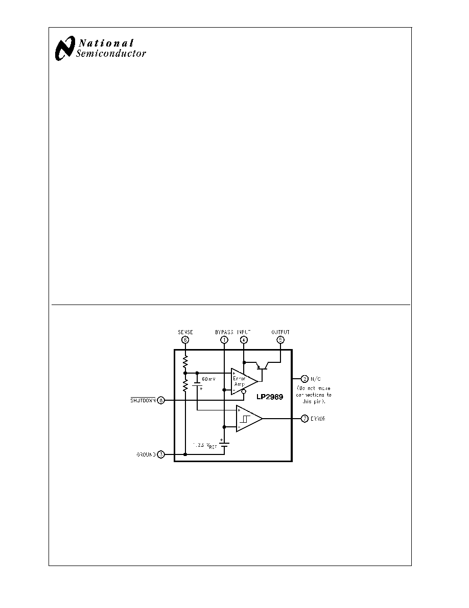
Block Diagram
10135701
VIP
TM
is a trademark of National Semiconductor Corporation.
February 2005
LP2989L
V
Micropower
500
mA
Low
Noise
Low
Dropout
Regulator
for
Output
V
oltages
<
2V
Designed
for
Use
with
V
ery
Low
ESR
Output
Capacitors
© 2005 National Semiconductor Corporation
DS101357
www.national.com
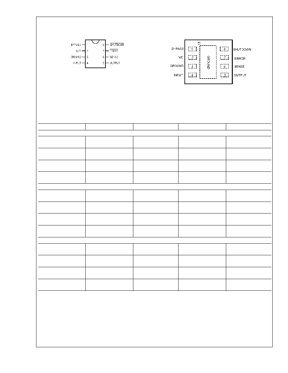
Connection Diagrams
Surface Mount Packages:
8 Lead LLP Surface Mount Package
10135702
SO-8/Mini SO-8 Package
See NS Package Drawing Numbers M08A/MUA08A
10135750
Top View
See NS Package Number LDC08A
Ordering Information
TABLE 1. Package Marking and Ordering Information
Output Voltage
Grade
Order Information
Package Marking
Supplied as:
8 Lead LLP
1.8
A
LP2989AILD-1.8
L01EA
1000 Units on Tape and
Reel
1.8
A
LP2989AILDX-1.8
L01EA
4500 Units on Tape and
Reel
1.8
STD
LP2989ILD-1.8
L01EAB
1000 Units on Tape and
Reel
1.8
STD
LP2989ILDX-1.8
L01EAB
4500 Units on Tape and
Reel
SO-8 (M)
1.8
A
LP2989AIMX-1.8
2989AIM1.8
2500 Units on Tape and
Reel
1.8
A
LP2989AIM-1.8
2989AIM1.8
Shipped in Anti-Static
Rails
1.8
STD
LP2989IMX-1.8
2989IM1.8
2500 Units on Tape and
Reel
1.8
STD
LP298IM-1.8
2989IM1.8
Shipped in Anti-Static
Rails
8 Lead MSOP (MM)
1.8
A
LP2989AIMMX-1.8
LA5A
3500 Units on Tape and
Reel
1.8
A
LP2989AIMM-1.8
LA5A
1000 Units on Tape and
Reel
1.8
STD
LP2989IMMX-1.8
LA5B
3500 Units on Tape and
Reel
1.8
STD
LP2989IMM-1.8
LA5B
1000 Units on Tape and
Reel
For output voltages
2V, see LP2989 datasheet.
LP2989L
V
www.national.com
2
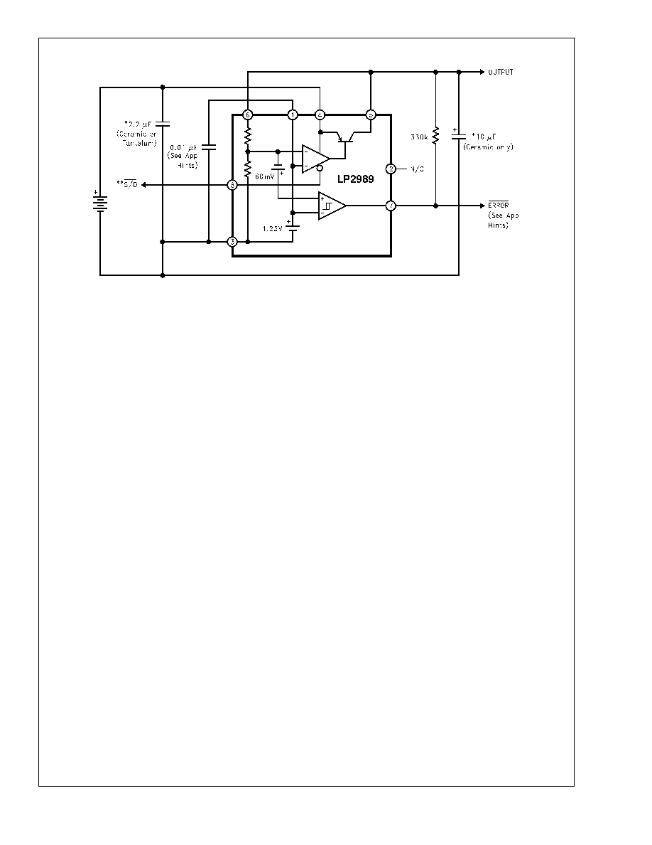
Basic Application Circuit
10135703
*Capacitance values shown are minimum required to assure stability, but may be increased without limit. Larger output capacitor provides improved dynamic
response.
**Shutdown must be actively terminated (see App. Hints). Tie to INPUT (Pin4) if not used.
LP2989L
V
www.national.com
3
Absolute Maximum Ratings
(Note 1)
If Military/Aerospace specified devices are required,
please contact the National Semiconductor Sales Office/
Distributors for availability and specifications.
Storage Temperature Range
-65°C to +150°C
Operating Junction
Temperature
Range
-40°C to +125°C
Lead Temperature
(Soldering, 5
seconds)
260°C
ESD Rating (Note 2)
2 kV
Power Dissipation (Note 3)
Internally Limited
Input Supply Voltage
(Survival)
-0.3V to +16V
Input Supply Voltage
(Operating)
2.1V to +16V
Sense Pin
-0.3V to +6V
Output Voltage
(Survival)
(Note 4)
-0.3V to +16V
I
OUT
(Survival)
Short Circuit
Protected
Input-Output Voltage
(Survival)
(Note 5)
-0.3V to +16V
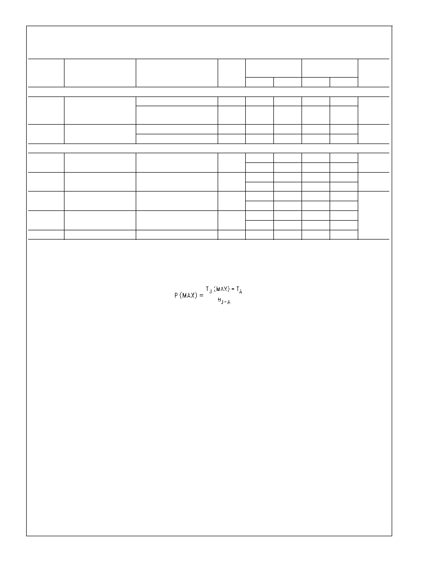
Electrical Characteristics
Limits in standard typeface are for T
J
= 25°C, and limits in boldface type apply over the full operating temperature range. Un-
less otherwise specified: V
IN
= V
O
(NOM) + 1V, I
L
= 1 mA, C
OUT
= 10 µF, C
IN
= 2.2 µF, V
S/D
= 2V.
Symbol
Parameter
Conditions
Typical
LP2989AI-X.X
(Note 6)
LP2989I-X.X
(Note 6)
Units
Min
Max
Min
Max
V
O
Output Voltage
Tolerance
-0.75
0.75
-1.25
1.25
%V
NOM
1 mA
<
I
L
<
500 mA
V
O
(NOM) + 1V
V
IN
16V
-1.5
1.5
-2.5
2.5
-4.0
2.5
-5.0
3.5
1 mA
<
I
L
<
500 mA
V
O
(NOM) + 1V
V
IN
16V
-25°C
T
J
125°C
-3.5
2.5
-4.5
3.5
Output Voltage Line
Regulation
V
O
(NOM) + 1V
V
IN
16V
0.005
0.014
0.014
%/V
0.032
0.032
Load Regulation
1 mA
<
I
L
<
500 mA
0.4
%V
NOM
V
IN
(min)
Minimum Input Voltage
Required To Maintain
Output Regulation
V
OUT
= 1.8
I
L
50 mA
1.96
V
V
OUT
= 1.8
I
L
= 250 mA
1.98
V
OUT
= 1.8
I
L
= 500 mA
2.11
I
GND
Ground Pin Current
I
L
= 100 µA
110
175
175
µA
200
200
I
L
= 200 mA
1
2
2
mA
3.5
3.5
I
L
= 500 mA
3
6
6
9
9
V
S/D
<
0.18V
0.5
2
2
µA
V
S/D
<
0.4V
0.05
0.8
0.8
I
O
(PK)
Peak Output Current
V
OUT
V
O
(NOM) - 5%
800
600
600
mA
I
O
(MAX)
Short Circuit Current
R
L
= 0 (Steady State) (Note
8)
1000
e
n
Output Noise Voltage
(RMS)
BW = 100 Hz to 100 kHz,
C
BYPASS
= .01 µF
18
µV(RMS)
Ripple Rejection
f = 1 kHz
60
dB
Output Voltage
Temperature Coefficient
(Note 7)
20
ppm/°C
LP2989L
V
www.national.com
4
Electrical Characteristics
(Continued)
Limits in standard typeface are for T
J
= 25°C, and limits in boldface type apply over the full operating temperature range. Un-
less otherwise specified: V
IN
= V
O
(NOM) + 1V, I
L
= 1 mA, C
OUT
= 10 µF, C
IN
= 2.2 µF, V
S/D
= 2V.
Symbol
Parameter
Conditions
Typical
LP2989AI-X.X
(Note 6)
LP2989I-X.X
(Note 6)
Units
Min
Max
Min
Max
SHUTDOWN INPUT
V
S/D
S/D Input Voltage
V
H
= O/P ON
1.4
1.6
1.6
V
V
L
= O/P OFF
I
IN
2 µA
0.50
0.18
0.18
I
S/D
S/D Input Current
V
S/D
= 0
0.001
-1
-1
µA
V
S/D
= 5V
5
15
15
ERROR COMPARATOR
I
OH
Output "HIGH" Leakage
V
OH
= 16V
0.001
1
1
µA
2
2
V
OL
Output "LOW" Voltage
V
OUT
= V
O
(NOM) - 0.5V
I
O
(COMP) = 150 µA
150
220
220
mV
350
350
V
THR
(MAX)
Upper Threshold
Voltage
-4.8
-6.0
-3.5
-6.0
-3.5
%V
OUT
-8.3
-2.5
-8.3
-2.5
V
THR
(MIN)
Lower Threshold
Voltage
-6.6
-8.9
-4.9
-8.9
-4.9
-13.0
-3.0
-13.0
-3.0
HYST
Hysteresis
2.0
Note 1: Absolute Maximum Ratings indicate limits beyond which damage to the component may occur. Electrical specifications do not apply when operating the
device outside of its rated operating conditions.
Note 2: ESD testing was performed using Human Body Model, a 100 pF capacitor discharged through a 1.5 k
resistor.
Note 3: The maximum allowable power dissipation is a function of the maximum junction temperature, T
J
(MAX), the junction-to-ambient thermal resistance,
J-A
,
and the ambient temperature, T
A
. The maximum allowable power dissipation at any ambient temperature is calculated using:
The value of
J-A
for the SO-8 (M) package is 160°C/W and the mini SO-8 (MM) package is 200°C/W. The value
J-A
for the LLP (LD) package is specifically
dependent on PCB trace area, trace material, and the number of layers and thermal vias. For improved thermal resistance and power dissipation for the LLP
package, refer to Application Note AN-1187.Exceeding the maximum allowable power dissipation will cause excessive die temperature, and the regulator will go into
thermal shutdown.
Note 4: If used in a dual-supply system where the regulator load is returned to a negative supply, the LP2989LV output must be diode-clamped to ground.
Note 5: The output PNP structure contains a diode between the V
IN
and V
OUT
terminals that is normally reverse-biased. Forcing the output above the input will turn
on this diode and may induce a latch-up mode which can damage the part (see Application Hints).
Note 6: Limits are 100% production tested at 25°C. Limits over the operating temperature range are guaranteed through correlation using Statistical Quality Control
(SQC) methods. The limits are used to calculate National's Average Outgoing Quality Level (AOQL).
Note 7: Temperature coefficient is defined as the maximum (worst-case) change divided by the total temperature range.
Note 8: See Typical Performance Characteristics curves.
LP2989L
V
www.national.com
5
Document Outline