TL H 5066
MF5
Universal
Monolithic
Switched
Capacitor
Filter
February 1995
MF5 Universal Monolithic Switched Capacitor Filter
General Description
The MF5 consists of an extremely easy to use general pur-
pose CMOS active filter building block and an uncommitted
op amp The filter building block together with an external
clock and a few resistors can produce various second order
functions The filter building block has 3 output pins One of
the output pins can be configured to perform highpass all-
pass or notch functions and the remaining 2 output pins
perform bandpass and lowpass functions The center fre-
quency of the filter can be directly dependent on the clock
frequency or it can depend on both clock frequency and
external resistor ratios The uncommitted op amp can be
used for cascading purposes for obtaining additional all-
pass and notch functions or for various other applications
Higher order filter functions can be obtained by cascading
several MF5s or by using the MF5 in conjuction with the
MF10 (dual switched capacitor filter building block) The
MF5 is functionally compatible with the MF10 Any of the
classical filter configurations (such as Butterworth Bessel
Cauer and Chebyshev) can be formed
Features
Y
Low cost
Y
14-pin DIP or 14-pin Surface Mount (SO) wide-body
package
Y
Easy to use
Y
Clock to center frequency ratio accuracy
g
0 6%
Y
Filter cutoff frequency stability directly dependent on
external clock quality
Y
Low sensitivity to external component variations
Y
Separate highpass (or notch or allpass) bandpass low-
pass outputs
Y
f
o
c
Q range up to 200 kHz
Y
Operation up to 30 kHz (typical)
Y
Additional uncommitted op-amp
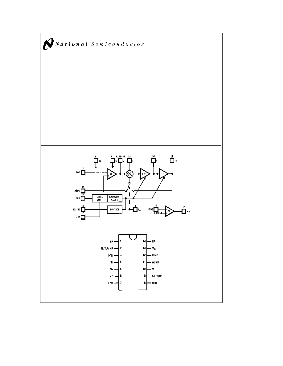
Block and Connection Diagrams
TL H 5066 � 1
All Packages
TL H 5066 � 2
Top View
Order Number MF5CN
See NS Package Number N14A
Order Number MF5CWM
See NS Package Number M14B
C1995 National Semiconductor Corporation
RRD-B30M115 Printed in U S A

Absolute Maximum Ratings
If Military Aerospace specified devices are required
please contact the National Semiconductor Sales
Office Distributors for availability and specifications
Supply Voltage (V
a
b
V
b
)
14V
Power Dissipation T
A
e
25 C (note 1)
500 mW
Storage Temp
150 C
Soldering Information
N Package
10 sec
260 C
SO Package
Vapor phase (60 sec )
215 C
Infrared (15 sec )
220 C
See AN-450 ``Surface Mounting Methods and Their Effect
on Product Reliability'' for other methods of soldering sur-
face mount devices
Input Voltage (any pin)
V
b s
V
in
s
V
a
Operating Temp Range
T
MIN
s
T
A
s
T
MAX
MF5CN MF5CWM
0 C
s
T
A
s
70 C
Electrical Characteristics
V
a
e
5V
g
0 5% V
b
e b
5V
g
0 5% unless otherwise noted Boldface limits
apply over temperature T
MIN
s
T
A
s
T
MAX
For all other limits T
A
e
25 C
Typical
Tested
Design
Parameter
Conditions
(Note 6)
Limit
Limit
Units
(Note 7)
(Note 8)
Supply Voltage
Min
8
V
(V
a
b
V
b
)
Max
14
V
Maximum Supply Current
Clock applied to Pin 8
4 5
6 0
mA
No Input Signal
Clock
Filter Output
10
mV
Feedthrough
Op-amp Output
10
mV
Filter Electrical Characteristics
V
a
e
5V
g
0 5% V
b
e b
5V
g
0 5% unless otherwise noted Boldface
limits apply over temperature T
MIN
s
T
A
s
T
MAX
For all other limits T
A
e
25 C
Typical
Tested
Design
Parameter
Conditions
(Note 6)
Limit
Limit
Units
(Note 7)
(Note 8)
Center Frequency
Max
30
20
kHz
Range (f
o
)
Min
0 1
0 2
Hz
Clock Frequency
Max
1 5
1 0
MHz
Range (f
CLK
)
Min
5 0
10
Hz
Clock to Center
Ideal
V
pin9
e a
5V
50 11
g
0 2%
50 11
g
1 5%
Frequency Ratio
Q
e
10
F
CLK
e
250 kHz
(f
CLK
f
o
)
Mode 1
V
pin9
e b
5V
100 04
g
0 2%
100 04
g
1 5%
F
CLK
e
500 kHz
f
CLK
f
o
Temp
V
pin9
e a
5V
g
10
ppm C
Coefficient
(50 1 CLK ratio)
V
pin9
e b
5V
g
20
ppm C
(100 1 CLK ratio)
Q Accuracy (Max)
Ideal
V
pin9
e a
5V
g
10
%
(Note 2)
Q
e
10
F
CLK
e
250 kHz
Mode 1
V
pin9
e b
5V
g
10
%
F
CLK
e
500 kHz
Q Temperature
V
pin9
e a
5V
b
200
ppm C
Coefficient
(50 1 CLK ratio)
V
pin9
e b
5V
b
70
ppm C
(100 1 CLK ratio)
DC Lowpass Gain
Mode 1
g
0 2
dB
Accuracy (Max)
R1
e
R2
e
10 kX
DC Offset
V
os1
g
5 0
mV
Voltage (Max)
V
os2
V
pin9
e a
5V
b
185
mV
V
os3
(50 1 CLK ratio)
a
115
mV
(Note 3)
V
os2
V
pin9
e b
5V
b
310
mV
V
os3
(100 1 CLK ratio)
a
240
mV
2

Filter Electrical Characteristics
V
a
e
5V
g
0 5% V
b
e b
5V
g
0 5% unless otherwise noted Boldface
limits apply over temperature T
MIN
s
T
A
s
T
MAX
For all other limits T
A
e
25 C (Continued)
Typical
Tested
Design
Parameter
Conditions
(Note 6)
Limit
Limit
Units
(Note 7)
(Note 8)
Output
BP LP pins
RL
e
5 kX
g
4 0
g
3 8
V
Swing (Min)
N AP HP pin
RL
e
3 5 kX
g
4 2
g
3 8
V
V
pin9
e a
5V
83
dB
Dynamic Range
(50 1 CLK ratio)
(Note 4)
V
pin9
e b
5V
80
dB
(100 1 CLK ratio)
Maximum Output Short Circuit
Source
20
mA
Current (Note 5)
Sink
3 0
mA
OP-AMP Electrical Characteristics
V
a
e a
5V
g
0 5% V
b
e b
5V
g
0 5% unless other noted Bold-
face limits apply over temperature T
MIN
s
T
A
s
T
MAX
For all other limits T
A
e
25 C
Typical
Tested
Design
Parameter
Conditions
(Note 6)
Limit
Limit
Units
(Note 7)
(Note 8)
Gain Bandwidth Product
2 5
MHz
Output Voltage Swing (Min)
RL
e
3 5 kX
g
4 2
g
3 8
V
Slew Rate
7 0
V ms
DC Open-Loop Gain
80
db
Input Offset Voltage (Max)
g
5 0
g
20
mV
Input Bias Current
10
pA
Maximum Output
Source
20
mA
Short Circuit
Current (Note 5)
Sink
3 0
mA
Logic Input Characteristics
Boldface limits apply over temperature T
MIN
s
T
A
s
T
MAX
All other limits T
A
e
25 C
Typical
Tested
Design
Parameter
Conditions
(Note 6)
Limit
Limit
Units
(Note 7)
(Note 8)
CMOS Clock
Min Logical ``1''
3 0
V
Input
Input Voltage
V
a
e a
5V V
b
e b
5V
Max Logical ``0''
V
L Sh
e
0V
b
3 0
V
Input Voltage
Min Logical ``1''
8 0
V
Input Voltage
V
a
e a
10V V
b
e
0V
Max Logical ``0''
V
L Sh
e a
5V
2 0
V
Input Voltage
TTL Clock
Min Logical ``1''
2 0
V
Input
Input Voltage
V
a
e a
5V V
b
e b
5V
Max Logical ``0''
V
L Sh
e
0V
0 8
V
Input Voltage
Note 1
The typical junction-to-ambient thermal resistance (i
JA
) of the 14 pin N package is 160 C W and 82 C W for the M package
Note 2
The accuracy of the Q value is a function of the center frequency (f
o
) This is illustrated in the curves under the heading ``Typical Performance
Characteristics''
Note 3
V
os1
V
os2
and V
os3
refer to the internal offsets as discussed in the Application Information section 3 4
Note 4
For
g
5V supplies the dynamic range is referenced to 2 82V rms (4V peak) where the wideband noise over a 20 kHz bandwidth is typically 200 mV rms for
the MF5 with a 50 1 CLK ratio and 280 mV rms for the MF5 with a 100 1 CLK ratio
Note 5
The short circuit source current is measured by forcing the output that is being tested to its maximum positive voltage swing and then shorting that output to
the negative supply The short circuit sink current is measured by forcing the output that is being tested to its maximum negative voltage swing and then shorting
that output to the positive supply These are the worst case conditions
Note 6
Typicals are at 25 C and represent most likely parametric norm
Note 7
Guaranteed and 100% tested
Note 8
Guaranteed but not 100% tested These limits are not used to calculate outgoing quality levels
3

Pin Description
LP(14) BP(1)
The second order lowpass bandpass
N AP HP(2)
and notch allpass highpass outputs The
LP and BP outputs can typically sink 1 mA
and source 3 mA The N AP HP output
can typically sink 1 5 mA and source 3
mA Each output typically swings to within
1V of each supply
INV1(3)
The inverting input of the summing op
amp of the filter This is a high impedance
input but the non-inverting input is
internally tied to AGND making INV1
behave like a summing junction (low
impedance current input)
S1(4)
S1 is a signal input pin used in the allpass
filter configurations (see modes 4 and 5)
The pin should be driven with a source
impedance of less than 1 kX If S1 is not
driven with a signal it should be tied to
AGND (mid-supply)
SA(5)
This pin activates a switch that connects
one of the inputs of the filter's second
summer to either AGND (SA tied to V
b
)
or to the lowpass (LP) output (SA tied to
V
a
) This offers the flexibility needed for
configuring the filter in its various modes
of operation
50 100(9)
This pin is used to set the internal clock to
center frequency ratio (f
CLK
f
o
) of the
filter By tying the pin to V
a
an f
CLK
f
o
ratio of about 50 1 (typically 50 11
g
0 2%) is obtained Tying the 50 100 pin to
either AGND or V
b
will set the f
CLK
f
o
ratio to about 100 1 (typically 100 04
g
0 2%)
AGND(11)
This is the analog ground pin This pin
should be connected to the system
ground for dual supply operation or biased
to mid-supply for single supply operation
For a further discussion of mid-supply
biasing techniques see the Applications
Information (Section 3 2) For optimum
filter performance a ``clean'' ground must
be provided
V
a
(6) V
b
(10)
These are the positive and negative
supply pins The MF5 will operate over a
total supply range of 8V to 14V
Decoupling the supply pins with 0 1 mF
capacitors is highly recommended
CLK(8)
This is the clock input for the filter CMOS
or TTL logic level clocks can be
accomodated by setting the L Sh pin to
the levels described in the L Sh pin
description For optimum filter
performance a 50% duty cycle clock is
recommended for clock frequencies
greater than 200 kHz This gives each op
amp the maximum amount of time to
settle to a new sampled input
L Sh(7)
This pin allows the MF5 to accommodate
either CMOS or TTL logic level clocks For
dual supply operation (i e
g
5V) a CMOS
or TTL logic level clock can be accepted if
the L Sh pin is tied to mid-supply (AGND)
which should be the system ground
For single supply operation the L Sh pin
should be tied to mid-supply (AGND) for a
CMOS logic level clock The mid-supply
bias should be a very low impedance
node See Applications Information for
biasing techniques For a TTL logic level
clock the L Sh pin should be tied to V
b
which should be the system ground
INV2(12)
This is the inverting input of the
uncommitted op amp This is a very high
impedance input but the non-inverting
input is internally tied to AGND making
INV2 behave like a summing junction
(low-impedance current input)
Vo2(13)
This is the output of the uncommitted op
amp It will typically sink 1 5 mA and
source 3 0 mA It will typically swing to
within 1V of each supply
Typical Performance Characteristics
Deviation of
F
CLK
F
o
vs Nominal Q
Deviation of
F
CLK
F
o
vs Nominal Q
OPAMP Output Voltage
Swing vs Temperature
TL H 5066 � 3
4
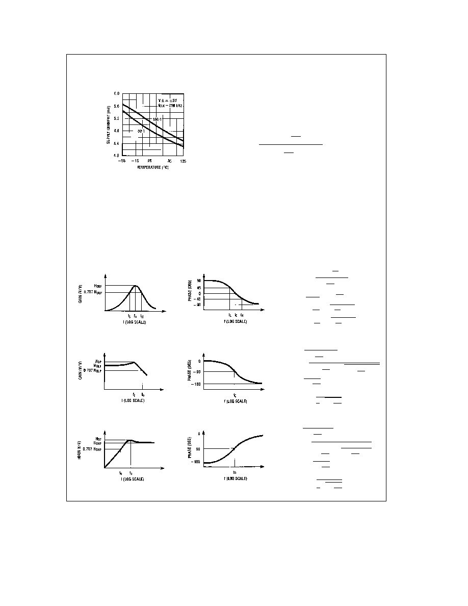
Typical Performance
Characteristics
(Continued)
Supply Current vs Temperature
TL H 5066 � 4
1 0 Definitions of Terms
f
CLK
the frequency of the external clock signal applied to
pin 8
f
o
center frequency of the second order function complex
pole pair f
o
is measured at the bandpass output of the MF5
and is the frequency of maximum bandpass gain (
Figure 1 )
f
notch
the frequency of minimum (ideally zero) gain at the
notch output
f
z
the center frequency of the second order complex zero
pair if any If f
z
is different from f
o
and if Q
z
is high it can be
observed as the frequency of a notch at the allpass output
(
Figure 10 )
Q
``quality factor'' of the 2nd order filter Q is measured at
the bandpass output of the MF5 and is equal to f
o
divided by
the
b
3dB bandwidth of the 2nd order bandpass filter (
Fig-
ure 1 ) The value of Q determines the shape of the 2nd
order filter responses as shown in
Figure 6
Q
z
the quality factor of the second order complex zero pair
if any Q
z
is related to the allpass characteristic which is
written
H
AP
(s)
e
H
OAP
s
2
b
s
0
o
Q
z
a
0
o
2
J
s
2
a
s
0
o
Q
a
0
o
2
where Q
z
e
Q for an all-pass response
H
OBP
the gain (in V V) of the bandpass output at f
e
f
o
H
OLP
the gain (in V V) of the lowpass output as f
x
0 Hz
(
Figure 2 )
H
OHP
the gain (in V V) of the highpass output as
f
x
f
clk
2 (
Figure 3 )
H
ON
the gain (in V V) of the notch output as f
x
0 Hz and
as f
x
f
clk
2 when the notch filter has equal gain above
and below the center frequency (
Figure 4 ) When the low-
frequency gain differs from the high-frequency gain as in
modes 2 and 3a (
Figures 11 and 8 ) the two quantities be-
low are used in place of H
ON
H
ON1
the gain (in V V) of the notch output as f
x
0 Hz
H
ON2
the gain (in V V) of the notch output as f
x
f
clk
2
(a)
TL H 5066 � 5
(b)
TL H 5066 � 6
H
BP
(s)
e
H
OBP
0
o
Q
s
s
2 a
s
0
o
Q
a
0
o
2
Q
e
f
o
f
H
b
f
L
f
o
e
0
f
L
f
H
f
L
e
f
o
b
1
2Q
a
0
1
2Q
J
2
a
1
J
f
H
e
f
o
1
2Q
a
0
1
2Q
J
2
a
1
J
0
o
e
2qf
o
FIGURE 1 2nd-Order Bandpass Response
(a)
TL H 5066 � 7
(b)
TL H 5066 � 8
H
LP
(s)
e
H
OLP
0
o
2
s
2 a
s
0
o
Q
a
0
o
2
f
c
e
f
o
c
0
1
b
1
2Q
2
J
a
0
1
b
1
2Q
2
J
2
a
1
f
p
e
f
o
0
1
b
1
2Q
2
H
OP
e
H
OLP
c
1
1
Q
0
1
b
1
4Q
2
FIGURE 2 2nd-Order Low-Pass Response
(a)
TL H 5066 � 9
FIGURE 3 2nd-Order High-Pass Response
(b)
TL H 5066 � 10
H
HP
(s)
e
H
OHP
s
2
s
2 a
s
0
o
Q
a
0
o
2
f
c
e
f
o
c
0
1
b
1
2Q
2
J
a
0
1
b
1
2Q
2
J
2
a
1
(
b
1
f
p
e
f
o
c
0
1
b
1
2Q
2
(
b
1
H
OP
e
H
OHP
c
1
1
Q
0
1
b
1
4Q
2
5