 | ÐлекÑÑоннÑй компоненÑ: MF5CWM | СкаÑаÑÑ:  PDF PDF  ZIP ZIP |
Äîêóìåíòàöèÿ è îïèñàíèÿ www.docs.chipfind.ru
TL H 5066
MF5
Universal
Monolithic
Switched
Capacitor
Filter
February 1995
MF5 Universal Monolithic Switched Capacitor Filter
General Description
The MF5 consists of an extremely easy to use general pur-
pose CMOS active filter building block and an uncommitted
op amp The filter building block together with an external
clock and a few resistors can produce various second order
functions The filter building block has 3 output pins One of
the output pins can be configured to perform highpass all-
pass or notch functions and the remaining 2 output pins
perform bandpass and lowpass functions The center fre-
quency of the filter can be directly dependent on the clock
frequency or it can depend on both clock frequency and
external resistor ratios The uncommitted op amp can be
used for cascading purposes for obtaining additional all-
pass and notch functions or for various other applications
Higher order filter functions can be obtained by cascading
several MF5s or by using the MF5 in conjuction with the
MF10 (dual switched capacitor filter building block) The
MF5 is functionally compatible with the MF10 Any of the
classical filter configurations (such as Butterworth Bessel
Cauer and Chebyshev) can be formed
Features
Y
Low cost
Y
14-pin DIP or 14-pin Surface Mount (SO) wide-body
package
Y
Easy to use
Y
Clock to center frequency ratio accuracy
g
0 6%
Y
Filter cutoff frequency stability directly dependent on
external clock quality
Y
Low sensitivity to external component variations
Y
Separate highpass (or notch or allpass) bandpass low-
pass outputs
Y
f
o
c
Q range up to 200 kHz
Y
Operation up to 30 kHz (typical)
Y
Additional uncommitted op-amp
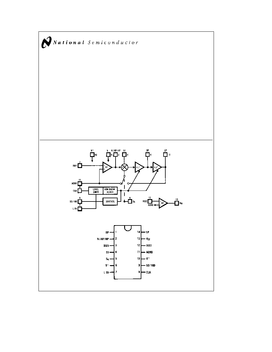
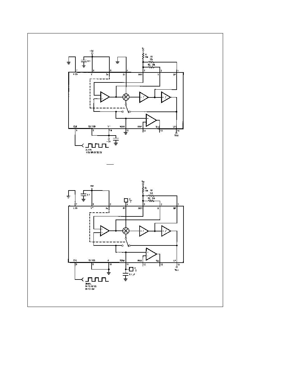
Block and Connection Diagrams
TL H 5066 1
All Packages
TL H 5066 2
Top View
Order Number MF5CN
See NS Package Number N14A
Order Number MF5CWM
See NS Package Number M14B
C1995 National Semiconductor Corporation
RRD-B30M115 Printed in U S A
Absolute Maximum Ratings
If Military Aerospace specified devices are required
please contact the National Semiconductor Sales
Office Distributors for availability and specifications
Supply Voltage (V
a
b
V
b
)
14V
Power Dissipation T
A
e
25 C (note 1)
500 mW
Storage Temp
150 C
Soldering Information
N Package
10 sec
260 C
SO Package
Vapor phase (60 sec )
215 C
Infrared (15 sec )
220 C
See AN-450 ``Surface Mounting Methods and Their Effect
on Product Reliability'' for other methods of soldering sur-
face mount devices
Input Voltage (any pin)
V
b s
V
in
s
V
a
Operating Temp Range
T
MIN
s
T
A
s
T
MAX
MF5CN MF5CWM
0 C
s
T
A
s
70 C
Electrical Characteristics
V
a
e
5V
g
0 5% V
b
e b
5V
g
0 5% unless otherwise noted Boldface limits
apply over temperature T
MIN
s
T
A
s
T
MAX
For all other limits T
A
e
25 C
Typical
Tested
Design
Parameter
Conditions
(Note 6)
Limit
Limit
Units
(Note 7)
(Note 8)
Supply Voltage
Min
8
V
(V
a
b
V
b
)
Max
14
V
Maximum Supply Current
Clock applied to Pin 8
4 5
6 0
mA
No Input Signal
Clock
Filter Output
10
mV
Feedthrough
Op-amp Output
10
mV
Filter Electrical Characteristics
V
a
e
5V
g
0 5% V
b
e b
5V
g
0 5% unless otherwise noted Boldface
limits apply over temperature T
MIN
s
T
A
s
T
MAX
For all other limits T
A
e
25 C
Typical
Tested
Design
Parameter
Conditions
(Note 6)
Limit
Limit
Units
(Note 7)
(Note 8)
Center Frequency
Max
30
20
kHz
Range (f
o
)
Min
0 1
0 2
Hz
Clock Frequency
Max
1 5
1 0
MHz
Range (f
CLK
)
Min
5 0
10
Hz
Clock to Center
Ideal
V
pin9
e a
5V
50 11
g
0 2%
50 11
g
1 5%
Frequency Ratio
Q
e
10
F
CLK
e
250 kHz
(f
CLK
f
o
)
Mode 1
V
pin9
e b
5V
100 04
g
0 2%
100 04
g
1 5%
F
CLK
e
500 kHz
f
CLK
f
o
Temp
V
pin9
e a
5V
g
10
ppm C
Coefficient
(50 1 CLK ratio)
V
pin9
e b
5V
g
20
ppm C
(100 1 CLK ratio)
Q Accuracy (Max)
Ideal
V
pin9
e a
5V
g
10
%
(Note 2)
Q
e
10
F
CLK
e
250 kHz
Mode 1
V
pin9
e b
5V
g
10
%
F
CLK
e
500 kHz
Q Temperature
V
pin9
e a
5V
b
200
ppm C
Coefficient
(50 1 CLK ratio)
V
pin9
e b
5V
b
70
ppm C
(100 1 CLK ratio)
DC Lowpass Gain
Mode 1
g
0 2
dB
Accuracy (Max)
R1
e
R2
e
10 kX
DC Offset
V
os1
g
5 0
mV
Voltage (Max)
V
os2
V
pin9
e a
5V
b
185
mV
V
os3
(50 1 CLK ratio)
a
115
mV
(Note 3)
V
os2
V
pin9
e b
5V
b
310
mV
V
os3
(100 1 CLK ratio)
a
240
mV
2
Filter Electrical Characteristics
V
a
e
5V
g
0 5% V
b
e b
5V
g
0 5% unless otherwise noted Boldface
limits apply over temperature T
MIN
s
T
A
s
T
MAX
For all other limits T
A
e
25 C (Continued)
Typical
Tested
Design
Parameter
Conditions
(Note 6)
Limit
Limit
Units
(Note 7)
(Note 8)
Output
BP LP pins
RL
e
5 kX
g
4 0
g
3 8
V
Swing (Min)
N AP HP pin
RL
e
3 5 kX
g
4 2
g
3 8
V
V
pin9
e a
5V
83
dB
Dynamic Range
(50 1 CLK ratio)
(Note 4)
V
pin9
e b
5V
80
dB
(100 1 CLK ratio)
Maximum Output Short Circuit
Source
20
mA
Current (Note 5)
Sink
3 0
mA
OP-AMP Electrical Characteristics
V
a
e a
5V
g
0 5% V
b
e b
5V
g
0 5% unless other noted Bold-
face limits apply over temperature T
MIN
s
T
A
s
T
MAX
For all other limits T
A
e
25 C
Typical
Tested
Design
Parameter
Conditions
(Note 6)
Limit
Limit
Units
(Note 7)
(Note 8)
Gain Bandwidth Product
2 5
MHz
Output Voltage Swing (Min)
RL
e
3 5 kX
g
4 2
g
3 8
V
Slew Rate
7 0
V ms
DC Open-Loop Gain
80
db
Input Offset Voltage (Max)
g
5 0
g
20
mV
Input Bias Current
10
pA
Maximum Output
Source
20
mA
Short Circuit
Current (Note 5)
Sink
3 0
mA
Logic Input Characteristics
Boldface limits apply over temperature T
MIN
s
T
A
s
T
MAX
All other limits T
A
e
25 C
Typical
Tested
Design
Parameter
Conditions
(Note 6)
Limit
Limit
Units
(Note 7)
(Note 8)
CMOS Clock
Min Logical ``1''
3 0
V
Input
Input Voltage
V
a
e a
5V V
b
e b
5V
Max Logical ``0''
V
L Sh
e
0V
b
3 0
V
Input Voltage
Min Logical ``1''
8 0
V
Input Voltage
V
a
e a
10V V
b
e
0V
Max Logical ``0''
V
L Sh
e a
5V
2 0
V
Input Voltage
TTL Clock
Min Logical ``1''
2 0
V
Input
Input Voltage
V
a
e a
5V V
b
e b
5V
Max Logical ``0''
V
L Sh
e
0V
0 8
V
Input Voltage
Note 1
The typical junction-to-ambient thermal resistance (i
JA
) of the 14 pin N package is 160 C W and 82 C W for the M package
Note 2
The accuracy of the Q value is a function of the center frequency (f
o
) This is illustrated in the curves under the heading ``Typical Performance
Characteristics''
Note 3
V
os1
V
os2
and V
os3
refer to the internal offsets as discussed in the Application Information section 3 4
Note 4
For
g
5V supplies the dynamic range is referenced to 2 82V rms (4V peak) where the wideband noise over a 20 kHz bandwidth is typically 200 mV rms for
the MF5 with a 50 1 CLK ratio and 280 mV rms for the MF5 with a 100 1 CLK ratio
Note 5
The short circuit source current is measured by forcing the output that is being tested to its maximum positive voltage swing and then shorting that output to
the negative supply The short circuit sink current is measured by forcing the output that is being tested to its maximum negative voltage swing and then shorting
that output to the positive supply These are the worst case conditions
Note 6
Typicals are at 25 C and represent most likely parametric norm
Note 7
Guaranteed and 100% tested
Note 8
Guaranteed but not 100% tested These limits are not used to calculate outgoing quality levels
3
Pin Description
LP(14) BP(1)
The second order lowpass bandpass
N AP HP(2)
and notch allpass highpass outputs The
LP and BP outputs can typically sink 1 mA
and source 3 mA The N AP HP output
can typically sink 1 5 mA and source 3
mA Each output typically swings to within
1V of each supply
INV1(3)
The inverting input of the summing op
amp of the filter This is a high impedance
input but the non-inverting input is
internally tied to AGND making INV1
behave like a summing junction (low
impedance current input)
S1(4)
S1 is a signal input pin used in the allpass
filter configurations (see modes 4 and 5)
The pin should be driven with a source
impedance of less than 1 kX If S1 is not
driven with a signal it should be tied to
AGND (mid-supply)
SA(5)
This pin activates a switch that connects
one of the inputs of the filter's second
summer to either AGND (SA tied to V
b
)
or to the lowpass (LP) output (SA tied to
V
a
) This offers the flexibility needed for
configuring the filter in its various modes
of operation
50 100(9)
This pin is used to set the internal clock to
center frequency ratio (f
CLK
f
o
) of the
filter By tying the pin to V
a
an f
CLK
f
o
ratio of about 50 1 (typically 50 11
g
0 2%) is obtained Tying the 50 100 pin to
either AGND or V
b
will set the f
CLK
f
o
ratio to about 100 1 (typically 100 04
g
0 2%)
AGND(11)
This is the analog ground pin This pin
should be connected to the system
ground for dual supply operation or biased
to mid-supply for single supply operation
For a further discussion of mid-supply
biasing techniques see the Applications
Information (Section 3 2) For optimum
filter performance a ``clean'' ground must
be provided
V
a
(6) V
b
(10)
These are the positive and negative
supply pins The MF5 will operate over a
total supply range of 8V to 14V
Decoupling the supply pins with 0 1 mF
capacitors is highly recommended
CLK(8)
This is the clock input for the filter CMOS
or TTL logic level clocks can be
accomodated by setting the L Sh pin to
the levels described in the L Sh pin
description For optimum filter
performance a 50% duty cycle clock is
recommended for clock frequencies
greater than 200 kHz This gives each op
amp the maximum amount of time to
settle to a new sampled input
L Sh(7)
This pin allows the MF5 to accommodate
either CMOS or TTL logic level clocks For
dual supply operation (i e
g
5V) a CMOS
or TTL logic level clock can be accepted if
the L Sh pin is tied to mid-supply (AGND)
which should be the system ground
For single supply operation the L Sh pin
should be tied to mid-supply (AGND) for a
CMOS logic level clock The mid-supply
bias should be a very low impedance
node See Applications Information for
biasing techniques For a TTL logic level
clock the L Sh pin should be tied to V
b
which should be the system ground
INV2(12)
This is the inverting input of the
uncommitted op amp This is a very high
impedance input but the non-inverting
input is internally tied to AGND making
INV2 behave like a summing junction
(low-impedance current input)
Vo2(13)
This is the output of the uncommitted op
amp It will typically sink 1 5 mA and
source 3 0 mA It will typically swing to
within 1V of each supply
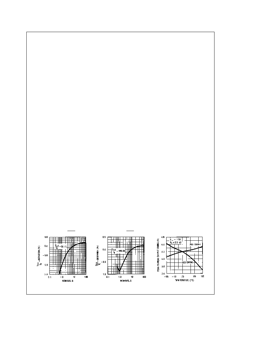
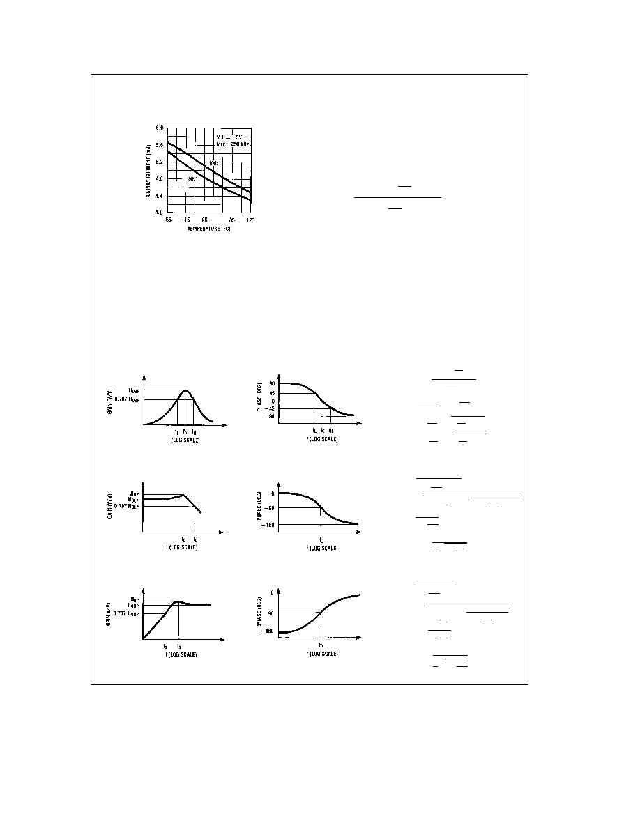
Typical Performance Characteristics
Deviation of
F
CLK
F
o
vs Nominal Q
Deviation of
F
CLK
F
o
vs Nominal Q
OPAMP Output Voltage
Swing vs Temperature
TL H 5066 3
4
Typical Performance
Characteristics
(Continued)
Supply Current vs Temperature
TL H 5066 4
1 0 Definitions of Terms
f
CLK
the frequency of the external clock signal applied to
pin 8
f
o
center frequency of the second order function complex
pole pair f
o
is measured at the bandpass output of the MF5
and is the frequency of maximum bandpass gain (
Figure 1 )
f
notch
the frequency of minimum (ideally zero) gain at the
notch output
f
z
the center frequency of the second order complex zero
pair if any If f
z
is different from f
o
and if Q
z
is high it can be
observed as the frequency of a notch at the allpass output
(
Figure 10 )
Q
``quality factor'' of the 2nd order filter Q is measured at
the bandpass output of the MF5 and is equal to f
o
divided by
the
b
3dB bandwidth of the 2nd order bandpass filter (
Fig-
ure 1 ) The value of Q determines the shape of the 2nd
order filter responses as shown in
Figure 6
Q
z
the quality factor of the second order complex zero pair
if any Q
z
is related to the allpass characteristic which is
written
H
AP
(s)
e
H
OAP
s
2
b
s
0
o
Q
z
a
0
o
2
J
s
2
a
s
0
o
Q
a
0
o
2
where Q
z
e
Q for an all-pass response
H
OBP
the gain (in V V) of the bandpass output at f
e
f
o
H
OLP
the gain (in V V) of the lowpass output as f
x
0 Hz
(
Figure 2 )
H
OHP
the gain (in V V) of the highpass output as
f
x
f
clk
2 (
Figure 3 )
H
ON
the gain (in V V) of the notch output as f
x
0 Hz and
as f
x
f
clk
2 when the notch filter has equal gain above
and below the center frequency (
Figure 4 ) When the low-
frequency gain differs from the high-frequency gain as in
modes 2 and 3a (
Figures 11 and 8 ) the two quantities be-
low are used in place of H
ON
H
ON1
the gain (in V V) of the notch output as f
x
0 Hz
H
ON2
the gain (in V V) of the notch output as f
x
f
clk
2
(a)
TL H 5066 5
(b)
TL H 5066 6
H
BP
(s)
e
H
OBP
0
o
Q
s
s
2 a
s
0
o
Q
a
0
o
2
Q
e
f
o
f
H
b
f
L
f
o
e
0
f
L
f
H
f
L
e
f
o
b
1
2Q
a
0
1
2Q
J
2
a
1
J
f
H
e
f
o
1
2Q
a
0
1
2Q
J
2
a
1
J
0
o
e
2qf
o
FIGURE 1 2nd-Order Bandpass Response
(a)
TL H 5066 7
(b)
TL H 5066 8
H
LP
(s)
e
H
OLP
0
o
2
s
2 a
s
0
o
Q
a
0
o
2
f
c
e
f
o
c
0
1
b
1
2Q
2
J
a
0
1
b
1
2Q
2
J
2
a
1
f
p
e
f
o
0
1
b
1
2Q
2
H
OP
e
H
OLP
c
1
1
Q
0
1
b
1
4Q
2
FIGURE 2 2nd-Order Low-Pass Response
(a)
TL H 5066 9
FIGURE 3 2nd-Order High-Pass Response
(b)
TL H 5066 10
H
HP
(s)
e
H
OHP
s
2
s
2 a
s
0
o
Q
a
0
o
2
f
c
e
f
o
c
0
1
b
1
2Q
2
J
a
0
1
b
1
2Q
2
J
2
a
1
(
b
1
f
p
e
f
o
c
0
1
b
1
2Q
2
(
b
1
H
OP
e
H
OHP
c
1
1
Q
0
1
b
1
4Q
2
5
1 0 Definition of Terms
(Continued)
TL H 5066 11
(a)
TL H 5066 12
(b)
H
N
(s)
e
H
ON
(s
2 a
0
o
2
)
s
2 a
s
0
o
Q
a
0
o
2
Q
e
f
o
f
H
b
f
L
f
o
e
0
f
L
f
H
f
L
e
f
o
b
1
2Q
a
0
1
2Q
J
2
a
1
J
f
H
e
f
o
1
2Q
a
0
1
2Q
J
2
a
1
J
FIGURE 4 2nd-Order Notch Response
TL H 5066 13
(a)
TL H 5066 14
(b)
H
AP
(s)
e
H
OAP
s
2 b
s0
o
Q
a
0
o
2
J
s
2 a
s0
o
Q
a
0
o
2
FIGURE 5 2nd-Order All-Pass Response
(a) Bandpass
(b) Low-Pass
(c) High-Pass
(d) Notch
(e) All-Pass
TL H 5066 15
FIGURE 6 Responses of various 2nd-order filters
as a function of Q Gains and center frequencies
are normalized to unity
6
2 0 Modes of Operation
The MF5 is a switched capacitor (sampled data) filter To
fully describe its transfer functions a time domain approach
is appropriate Since this is cumbersome and since the
MF5 closely approximates continuous filters the following
discussion is based on the well known frequency domain
Each MF5 can produce a full 2nd order function See Table
1 for a summary of the characteristics of the various modes
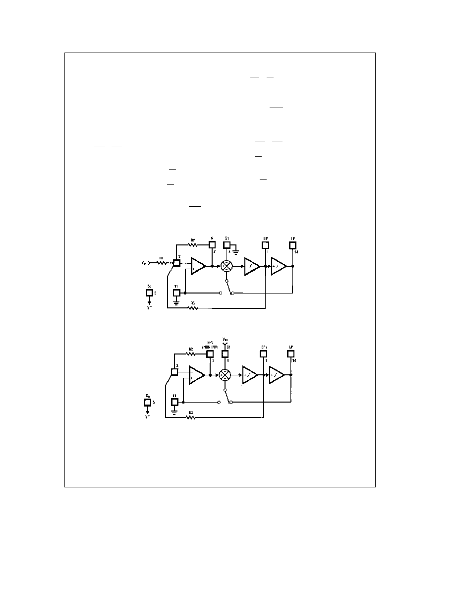
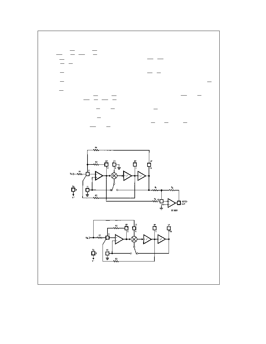
MODE 1 Notch 1 Bandpass Lowpass Outputs
f
notch
e
f
o
(See
Figure 7 )
f
o
e
center frequency of the complex pole pair
e
f
CLK
100
or
f
CLK
50
f
notch
e
center frequency of the imaginary zero pair
e
f
o
H
OLP
e
Lowpass gain (as f
x
0)
e b
R2
R1
H
OBP
e
Bandpass gain (at f
e
f
o
)
e b
R3
R1
H
ON
e
Notch output gain as f
x
0
f
x
f
CLK
2
(
e
b
R
2
R
1
Q
e
f
o
BW
e
R3
R2
BW
e
the
b
3 dB bandwidth of the bandpass output
Circuit dynamics
H
OLP
e
H
OBP
Q
or H
OBP
e
H
OLP
c
Q
e
H
ON
c
Q
H
OLP(peak)
j
Q
c
H
OLP
(for high Q's)
MODE 1a Non-Inverting BP LP (See
Figure 8 )
f
o
e
f
CLK
100
or
f
CLK
50
Q
e
R3
R2
H
OLP
e b
1 H
OLP(peak)
j
Q
c
H
OLP
(for high Q's)
H
OBP1
e b
R3
R2
H
OBP2
e
1 (non-inverting)
Circuit dynamics H
OBP1
e
Q
Note V
IN
should be driven from a low impedance (
k
1 kX)
TL H 5066 16
FIGURE 7 MODE 1
TL H 5066 17
FIGURE 8 MODE 1a
7
2 0 Modes of Operation
(Continued)
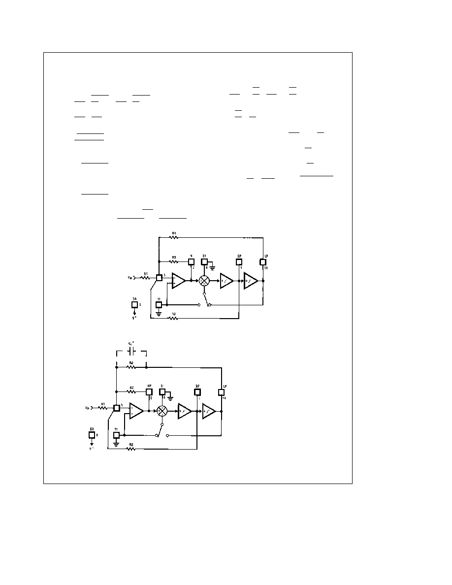
MODE 2 Notch 2 Bandpass Lowpass f
notch
k
f
o
(See
Figure 9 )
f
o
e
center frequency
e
f
CLK
100
0
R2
R4
a
1 or
f
CLK
50
0
R2
R4
a
1
f
notch
e
f
CLK
100
or
f
CLK
50
Q
e
quality factor of the complex pole pair
e 0
R2 R4
a
1
R2 R3
H
OLP
e
Lowpass output gain (as f
x
0)
e b
R2 R1
R2 R4
a
1
H
OBP
e
Bandpass output gain (at f
e
f
o
)
e b
R3 R1
H
ON1
e
Notch output gain (as f
x
0)
e b
R2 R1
R2 R4
a
1
H
ON2
e
Notch output gain
as f
x
f
CLK
2
J
e b
R2 R1
Filter dynamics H
OBP
e
Q
0
H
OLP
H
ON2
e
Q
0
H
ON1
H
ON2
MODE 3 Highpass Bandpass Lowpass Outputs
(See
Figure 10 )
f
o
e
f
CLK
100
c
0
R2
R4
or
f
CLK
50
c
0
R2
R4
Q
e
quality factor of the complex pole pair
e
0
R2
R4
c
R3
R2
H
OHP
e
Highpass gain
as f
x
f
CLK
2
J
e b
R2
R1
H
OBP
e
Bandpass gain (at f
e
f
o
)
e b
R3
R1
H
OLP
e
Lowpass gain (as f
x
0)
e b
R4
R1
Circuit dynamics
R2
R4
e
H
OHP
H
OLP
H
OBP
e
0
H
OHP
c
H
OLP
c
Q
H
OLP(peak)
j
Q
c
H
OLP
(for high Q's)
H
OHP(peak)
j
Q
c
H
OHP
(for high Q's)
TL H 5066 18
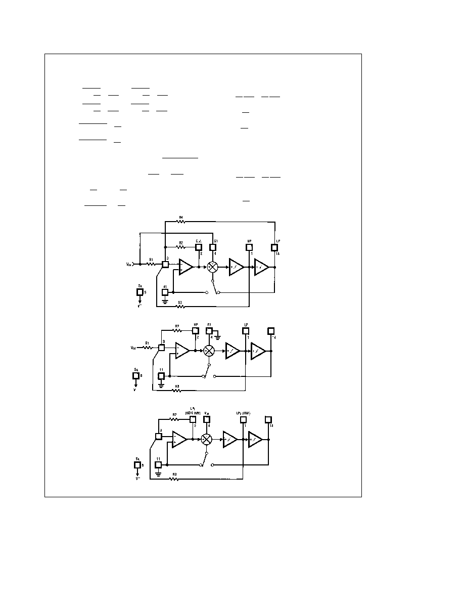
FIGURE 9 MODE 2
TL H 5066 19
FIGURE 10 MODE 3
In Mode 3 the feedback loop is closed around
the input summing amplifier the finite GBW prod-
uct of this op amp causes a slight Q enhance-
ment If this is a problem connect a small capaci-
tor (10 pF100 pF) across R4 to provide some
phase lead
8
2 0 Modes of Operation
(Continued)
MODE 3a HP BP LP and Notch with External Op amp
(See
Figure 11 )
f
o
e
f
CLK
100
c
0
R2
R4
or
f
CLK
50
c
0
R2
R4
Q
e
0
R2
R4
c
R3
R2
H
OHP
e b
R2
R1
H
OBP
e b
R3
R1
H
OLP
e b
R4
R1
f
n
e
notch frequency
e
f
CLK
100
0
R
h
R
l
or
f
CLK
50
0
R
h
R
l
H
on
e
gain of notch at f
e
f
o
e
Q
R
g
R
l
H
OLP
b
R
g
R
h
H
OHP
J
H
n1
e
gain of notch (as f
x
0)
e
R
g
R
l
c
H
OLP
H
n2
e
gain of notch
as f
x
f
CLK
2
J
e b
R
g
R
h
c
H
OHP
MODE 4 Allpass Bandpass Lowpass Outputs (See
Figure 12 )
f
o
e
center frequency
e
f
CLK
100
or
f
CLK
50
f
z
e
center frequency of the complex zero pairjf
o
Q
e
f
o
BW
e
R3
R2
Q
z
e
quality factor of complex zero pair
e
R3
R1
For AP output make R1
e
R2
H
OAP
e
Allpass gain
at 0
k
f
k
f
CLK
2
J
e b
R2
R1
e b
1
H
OLP
e
Lowpass gain (as f
x
0)
e b
R2
R1
a
1
J
e b
2
H
OBP
e
Bandpass gain (at f
e
f
o
)
e b
R3
R2
1
a
R2
R1
J
e b
2
R3
R2
J
Circuit dynamics H
OBP
e
(H
OLP
)
c
Q
e
(H
OAP
a
1) Q
Due to the sampled data nature of the filter a slight mismatch of f
z
and f
o
occurs causing a 0 4 dB peaking around f
o
of the allpass filter amplitude
response (which theoretically should be a straight line) If this is unaccept-
able Mode 5 is recommended
TL H 5066 20
FIGURE 11 MODE 3a
TL H 5066 21
FIGURE 12 MODE 4
9
2 0 Modes of Operation
(Continued)
MODE 5 Numerator Complex Zeros BP LP
(See
Figure 13 )
f
o
e
0
1
a
R2
R4
c
f
CLK
100
or
0
1
a
R2
R4
c
f
CLK
50
f
z
e
0
1
b
R1
R4
c
f
CLK
100
or
0
1
b
R1
R4
c
f
CLK
50
Q
e
0
1
a
R2 R4
c
R3
R2
Q
z
e
0
1
b
R1 R4
c
R3
R1
H
0z1
e
gain at C Z output (as f
x
0 Hz)
e
b
R2 (R4
b
R1)
R1 (R4
a
R2)
H
0z2
e
gain at C Z output
as f
x
f
CLK
2
J
e
b
R2
R1
H
OBP
e b
e
R2
R1
a
1
J
c
R3
R2
H
OLP
e b
R2
a
R1
R2
a
R4
J
c
R4
R1
MODE 6a Single Pole HP LP Filter (See
Figure 14 )
f
c
e
cutoff frequency of LP or HP output
e
R2
R3
f
CLK
100
or
R2
R3
f
CLK
50
H
OLP
e b
R3
R1
H
OHP
e b
R2
R1
MODE 6b Single Pole LP Filter (Inverting and Non-
Inverting) (See
Figure 15 )
f
c
e
cutoff frequency of LP outputs
j
R2
R3
f
CLK
100
or
R2
R3
f
CLK
50
H
OLP1
e
1 (non-inverting)
H
OLP2
e b
R3
R2
TL H 5066 22
FIGURE 13 MODE 5
TL H 5066 23
FIGURE 14 MODE 6a
TL H 5066 24
FIGURE 15 MODE 6b
10
2 0 Modes of Operation
(Continued)
TABLE I Summary of Modes Realizable filter types (e g low-pass) denoted by asterisks Unless otherwise noted
gains of various filter outputs are inverting and adjustable by resistor ratios
Mode
BP
LP
HP
N
AP
Number of
Adjustable
Notes
resistors
f
CLK
f
o
1
3
No
(2)
May need input buf-
1a
H
OBP1e bQ
H
OLPe a1
2
No
fer Poor dynamics
H
OBP2e a1
for high Q
Yes (above
2
3
f
CLK
50 or
f
CLK
100)
Universal State-
3
4
Yes
Variable Filter Best
general-purpose mode
As above but also
3a
7
Yes
includes resistor-
tuneable notch
Gives Allpass res-
4
3
No
ponse with H
OAP
e b
1
and H
OLP
e b
2
Gives flatter allpass
5
4
response than above
if R
1
e
R
2
e
0 02R
4
6a
3
Single pole
(2)
6b
H
OLP
e a
1
2
Single pole
H
OLP2
e
b
R3
R2
3 0 Applications Information
The MF5 is a general-purpose second-order state variable
filter whose center frequency is proportional to the frequen-
cy of the square wave applied to the clock input (f
CLK
) By
connecting pin 9 to the appropriate DC voltage the filter
center frequency f
o
can be made equal to either f
CLK
100
or f
CLK
50 f
o
can be very accurately set (within
g
0 6%) by
using a crystal clock oscillator or can be easily varied over
a wide frequency range by adjusting the clock frequency If
desired the f
CLK
f
o
ratio can be altered by external resis-
tors as in
Figures 9 10 11 13 14 and 15 The filter Q and
gain are determined by external resistors
All of the five second-order filter types can be built using the
MF5 These are illustrated in
Figures 1 through 5 along with
their transfer functions and some related equations
Figure
6 shows the effect of Q on the shapes of these curves
When filter orders greater than two are desired two or more
MF5s can be cascaded The MF5 also includes an uncom-
mitted CMOS operational amplifier for additional signal pro-
cessing applications
3 1 DESIGN EXAMPLE
An example will help illustrate the MF5 design procedure
For the example we will design a 2nd order Butterworth
low-pass filter with a cutoff frequency of 200 Hz and a pass-
band gain of
b
2 The circuit will operate from a
g
5V power
supply and the clock amplitude will be
g
5v (CMOS) levels)
From
the
specifications
the
filter
parameters
are
f
o
e
200 Hz H
OLP
e b
2 and for Butterworth response
Q
e
0 707
In section 2 0 are several modes of operation for the MF5
each having different characteristics Some allow adjust-
ment of f
CLK
f
o
others produce different combinations of
filter types some are inverting while others are non-invert-
ing etc These characteristics are summarized in Table I To
keep the example simple we will use mode 1 which has
notch bandpass and lowpass outputs and inverts the sig-
nal polarity Three external resistors determine the filter's Q
and gain From the equations accompanying
Figure 7
Q
e
R
3
R
2
and the passband gain H
OLP
e b
R
2
R
1
Since
the input signal is driving a summing junction through R
1
the input impedance will be equal to R
1
Start by choosing a
value for R
1
10k is convenient and gives a reasonable input
impedance For H
OLP
e b
2 we have
R
2
e b
R
1
H
OLP
e
10k
c
2
e
20k
For Q
e
0 707 we have
R
3
e
R
2
Q
e
20k
c
0 707
e
14 14k Use 15k
For operation on
g
5V supplies V
a
is connected to
a
5V
V
b
to
b
5V and AGND to ground The power supplies
should be ``clean'' (regulated supplies are preferred) and
0 1 mF bypass capacitors are recommended
11
3 0 Applications Information
(Continued)
TL H 5066 25
FIGURE 16 2nd-Order Butterworth Low-Pass Filter of Design
Example For
f
CLK
f
0
e
50 Connect Pin 9 to
a
5V and
Change Clock Frequency to 10 kHz
TL H 5066 26
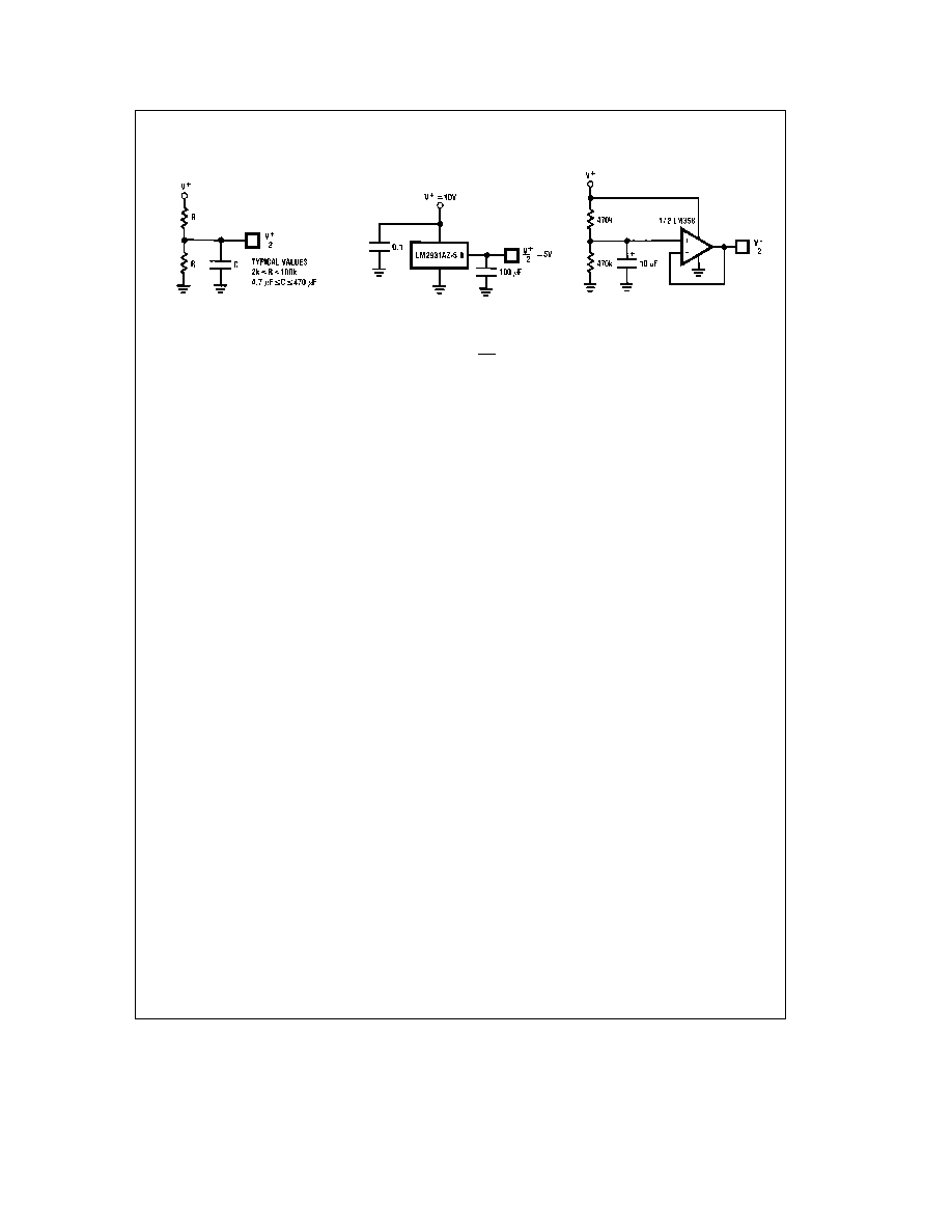
FIGURE 17 Butterworth Low-Pass Circuit of Example but Designed for Single-Supply Operation
12
3 0 Applications Information
(Continued)
TL H 5066 27
(a) Resistive Divider with
Decoupling Capaciter
TL H 5066 28
(b) Voltage Regulator
TL H 5066 29
(c) Operational Amplifier
with Divider
FIGURE 18 Three Ways of Generating
V
a
2
for Single-supply Operation
For a cutoff frequency of 200 Hz the external clock can be
either 10 kHz with pin 9 connected to V
a
(50 1) or 20 kHz
with pin 9 tied to A
GND
or V
b
(100 1) The voltage on the
Logic Level Shift pin (7) determines the logic threshold for
the clock input The threshold is approximately 2V higher
than the voltage applied to pin 7 Therefore when pin 7 is
grounded the clock logic threshold will be 2V making it
compatible with 0 5 volt TTL logic levels and
g
5 volt
CMOS levels Pin 7 should be connected to a clean low-im-
pedance (less than 1000X) voltage source
The complete circuit of the design example is shown for a
100 1 clock ratio in
Figure 16
3 2 SINGLE SUPPLY OPERATION
The MF5 can also operate with a single-ended power sup-
ply
Figure 17 shows the example filter with a single-ended
power supply V
a
is again connected to the positive power
supply (8 to 14 volts) and V
b
is connected to ground The
A
GND
pin must be tied to V
a
2 for single supply operation
This half-supply point should be very ``clean'' as any noise
appearing on it will be treated as an input to the filter It can
be derived from the supply voltage with a pair of resistors
and a bypass capacitor (
Figure 18a ) or a low-impedance
half-supply voltage can be made using a three-terminal volt-
age regulator or an operational amplifier (
Figures 18b and
18c ) The passive resistor divider with a bypass capacitor is
sufficient for many applications provided that the time con-
stant is long enough to reject any power supply noise It is
also important that the half-supply reference present a low
impedance to the clock frequency so at very low clock fre-
quencies the regulator or op-amp approaches may be pref-
erable because they will require smaller capacitors to filter
the clock frequency The main power supply voltage should
be clean (preferably regulated) and bypassed with 0 1mF
3 3 DYNAMIC CONSIDERATIONS
The maximum signal handling capability of the MF5 like
that of any active filter is limited by the power supply volt-
ages used The amplifiers in the MF5 are able to swing to
within about 1 volt of the supplies so the input signals must
be kept small enough that none of the outputs will exceed
these limits If the MF5 is operating on
g
5 volts for exam-
ple the outputs will clip at about 8V
p-p
The maximum input
voltage multiplied by the filter gain should therefore be less
than 8V
p-p
Note that if the filter has high Q the gain at the lowpass or
highpass outputs will be much greater than the nominal filter
gain (
Figure 6 ) As an example a lowpass filter with a Q of
10 will have a 20 dB peak in its amplitude response at f
o
If
the nominal gain of the filter H
OLP
is equal to 1 the gain at
f
o
will be 10 The maximum input signal at f
o
must therefore
be less than 800 mV
p-p
when the circuit is operated on
g
5
volt supplies
Also note that one output can have a reasonable small volt-
age on it while another is saturated This is most likely for a
circuit such as the notch in Mode 1 (
Figure 7 ) The notch
output will be very small at f
o
so it might appear safe to
apply a large signal to the input However the bandpass will
have its maximum gain at f
o
and can clip if overdriven If one
output clips the performance at the other outputs will be
degraded so avoid overdriving any filter section even ones
whose outputs are not being directly used Accompanying
Figures 7 through 15 are equations labeled ``circuit dynam-
ics'' which relate the Q and the gains at the various outputs
These should be consulted to determine peak circuit gains
and maximum allowable signals for a given application
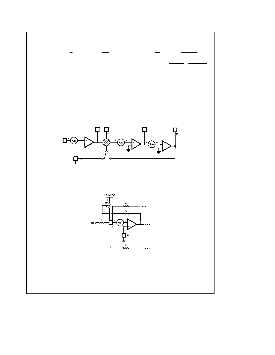
3 4 OFFSET VOLTAGE
The MF5's switched capacitor integrators have a higher
equivalent input offset voltage than would be found in a
typical continuous-time active filter integrator
Figure 19
shows an equivalent circuit of the MF5 from which the out-
put dc offsets can be calculated Typical values for these
offsets are
V
os1
e
opamp offset
e
g
5mV
V
os2
e b
185mV
50 1
b
310mV
100 1
V
os3
e a
115mV
50 1
a
240mV
100 1
The dc offset at the BP output is equal to the input offset of
the lowpass integrator (V
os3
) The offsets at the other out-
puts depend on the mode of operation and the resistor ra-
tios as described in the following expressions
13
3 0 Applications Information
(Continued)
Mode 1 and Mode 4
V
OS(N)
e
V
OS1
1
Q
a
1
a
H
OLP
J
b
V
OS3
Q
V
OS(BP)
e
V
OS3
V
OS(LP)
e
V
OS(N)
b
V
OS2
Mode 1a
V
OS
(N INV BP)
e
1
a
1
Q
J
V
OS1
b
V
OS3
Q
V
OS
(INV BP)
e
V
OS3
V
OS
(LP)
e
V
OS
(N INV BP)
b
V
OS2
Mode 2 and Mode 5
V
OS(N)
e
R2
Rp
a
1
J
V
OS1
c
1
1
a
R2 R4
a
V
OS2
1
1
a
R4 R2
b
V
OS3
Q
0
1
a
R2 R4
R
p
e
R1
R2
R4
V
OS(BP)
e
V
OS3
V
OS(LP)
e
V
OS(N)
b
V
OS2
Mode 3
V
OS(HP)
e
V
OS2
V
OS(BP)
e
V
OS3
V
OS(LP)
e b
R4
R2
R2
R3
V
OS3
a
V
OS2
J
a
b
R4
R2
1
a
R2
R
p
J
V
OS1
R
p
e
R1
R3
R4
TL H 5066 30
FIGURE 19 Block Diagram Showing MF5
Offset Voltage Sources
TL H 5066 31
FIGURE 20 Method for Trimming V
OS
See Text Section 3 4
14
3 0 Applications Information
(Continued)
For most applications the outputs are AC coupled and DC
offsets are not bothersome unless large signals are applied
to the filter input However larger offset voltages will cause
clipping to occur at lower ac signal levels and clipping at
any of the outputs will cause gain nonlinearities and will
change f
o
and Q When operating in Mode 3 offsets can
become excessively large if R
2
and R
4
are used to make
f
CLK
f
o
significantly higher than the nominal value especial-
ly if Q is also high An extreme example is a bandpass filter
having unity gain a Q of 20 and f
CLK
f
o
e
250 with pin 9
tied to V
b
(100 1 nominal) R
4
R
2
will therefore be equal to
6 25 and the offset voltage at the lowpass output will be
about
a
1 9V Where necessary the offset voltage can be
adjusted by using the circuit of
Figure 20 This allows adjust-
ment of V
os1
which will have varying effects on the different
outputs as described in the above equations Some outputs
cannot be adjusted this way in some modes however
(V
os(BP)
in modes 1a and 3 for example)
3 5 SAMPLED DATA SYSTEM CONSIDERATIONS
The MF5 is a sampled data filter and as such differs in
many ways from conventional continuous-time filters An im-
portant characteristic of sampled-data systems is their ef-
fect on signals at frequencies greater than one-half the
sampling frequency (The MF5's sampling frequency is the
same as its clock frequency) If a signal with a frequency
greater than one-half the sampling frequency is applied to
the input of a sampled data system it will be ``reflected'' to
a frequency less than one-half the sampling frequency
Thus an input signal whose frequency is f
s
2
a
100 Hz will
cause the system to respond as though the input frequency
was f
s
2 - 100 Hz This phenomenon is known as ``alias-
ing'' and can be reduced or eliminated by limiting the input
signal spectrum to less than f
s
2 This may in some cases
require the use of a bandwidth-limiting filter ahead of the
MF5 to limit the input spectrum However since the clock
frequency is much higher than the center frequency this will
often not be necessary
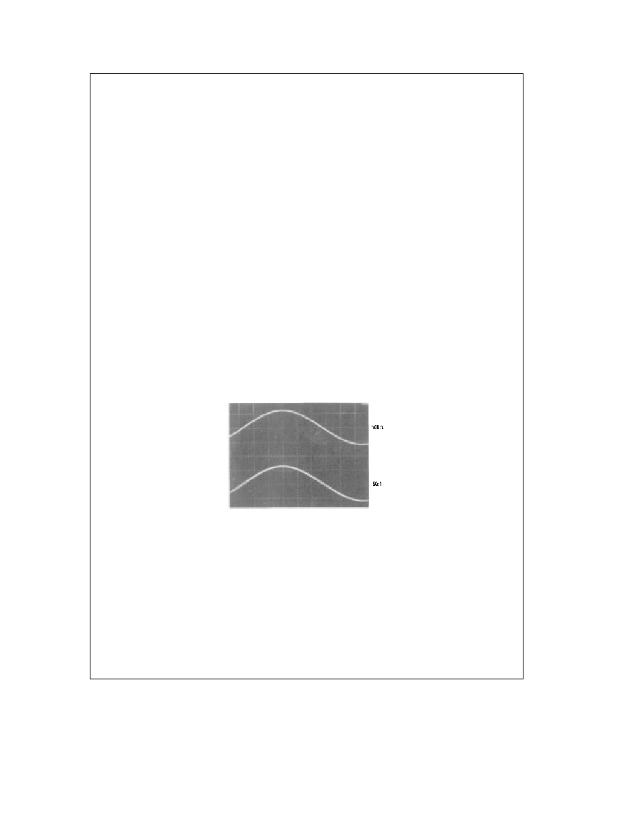
Another characteristic of sampled-data circuits is that the
output signal changes amplitude once every sampling peri-
od resulting in ``steps'' in the output voltage which occur at
the clock rate (
Figure 21 ) If necessary these can be
``smoothed'' with a simple R-C low-pass filter at the MF5
output
The ratio of f
CLK
to f
c
(normally either 50 1 or 100 1) will
also affect performance A ratio of 100 1 will reduce any
aliasing problems and is usually recommended for wide-
band input signals In noise sensitive applications however
a ratio of 50 1 may be better as it will result in 3 dB lower
output noise The 50 1 ratio also results in lower DC offset
voltages as discussed in 3 4
The accuracy of the f
CLK
f
o
ratio is dependent on the value
of Q This is illustrated in the curves under the heading
``Typical Performance Characteristics'' As Q is changed
the true value of the ratio changes as well Unless the Q is
low the error in f
CLK
f
o
will be small If the error is too large
for a specific application use a mode that allows adjustment
of the ratio with external resistors
It should also be noted that the product of Q and f
o
should
be limited to 300 kHz when f
o
k
5 kHz and to 200 kHz for
f
o
l
5 kHz
TL H 5066 32
FIGURE 21 The Sampled-Data Output Waveform
15
MF5
Universal
Monolithic
Switched
Capacitor
Filter
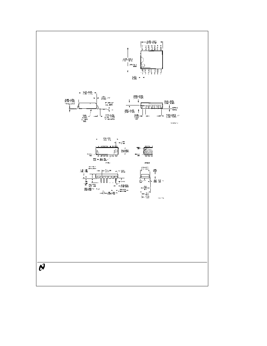
Physical Dimensions
inches (millimeters)
SO Package
Order Number MF5CWM
NS Package Number M14B
Molded Dual-In-Line Package (N)
Order Number MF5CN
NS Package Number N14A
LIFE SUPPORT POLICY
NATIONAL'S PRODUCTS ARE NOT AUTHORIZED FOR USE AS CRITICAL COMPONENTS IN LIFE SUPPORT
DEVICES OR SYSTEMS WITHOUT THE EXPRESS WRITTEN APPROVAL OF THE PRESIDENT OF NATIONAL
SEMICONDUCTOR CORPORATION As used herein
1 Life support devices or systems are devices or
2 A critical component is any component of a life
systems which (a) are intended for surgical implant
support device or system whose failure to perform can
into the body or (b) support or sustain life and whose
be reasonably expected to cause the failure of the life
failure to perform when properly used in accordance
support device or system or to affect its safety or
with instructions for use provided in the labeling can
effectiveness
be reasonably expected to result in a significant injury
to the user
National Semiconductor
National Semiconductor
National Semiconductor
National Semiconductor
Corporation
Europe
Hong Kong Ltd
Japan Ltd
1111 West Bardin Road
Fax (a49) 0-180-530 85 86
13th Floor Straight Block
Tel 81-043-299-2309
Arlington TX 76017
Email cnjwge tevm2 nsc com
Ocean Centre 5 Canton Rd
Fax 81-043-299-2408
Tel 1(800) 272-9959
Deutsch Tel (a49) 0-180-530 85 85
Tsimshatsui Kowloon
Fax 1(800) 737-7018
English
Tel (a49) 0-180-532 78 32
Hong Kong
Fran ais Tel (a49) 0-180-532 93 58
Tel (852) 2737-1600
Italiano
Tel (a49) 0-180-534 16 80
Fax (852) 2736-9960
National does not assume any responsibility for use of any circuitry described no circuit patent licenses are implied and National reserves the right at any time without notice to change said circuitry and specifications