 | –≠–ª–µ–∫—Ç—Ä–æ–Ω–Ω—ã–π –∫–æ–º–ø–æ–Ω–µ–Ω—Ç: MM5480 | –°–∫–∞—á–∞—Ç—å:  PDF PDF  ZIP ZIP |

TL F 6138
MM5480
LED
Display
Driver
February 1995
MM5480 LED Display Driver
General Description
The MM5480 is a monolithic MOS integrated circuit utilizing
N-channel metal gate low threshold enhancement mode
and ion-implanted depletion mode devices It utilizes the
MM5451 die packaged in a 28-pin package making it ideal
for a 3
digit display The MM5480 is designed to drive
common anode-separate cathode LED displays A single
pin controls the LED display brightness by setting a refer-
ence current through a variable resistor connected either to
V
DD
or to a separate supply of 11V maximum
Features
Y
Continuous brightness control
Y
Serial data input
Y
No load signal required
Y
Wide power supply operation
Y
TTL compatibility
Y
Alphanumeric capability
Y
3
digit displays
Applications
Y
COPS
TM
microcontrollers or microprocessor displays
Y
Industrial control indicator
Y
Relay driver
Y
Digital clock thermometer counter voltmeter
Y
Instrumentation readouts
Block Diagram
TL F 6138 ≠ 1
FIGURE 1
Connection Diagram
Dual-In-Line Package
TL F 6138 ≠ 2
Top View
FIGURE 2
Order Number MM5480N
See NS Package Number N28B
COPS
TM
microcontrollers is a trademark of National Semiconductor Corporation
C1995 National Semiconductor Corporation
RRD-B30M105 Printed in U S A

Absolute Maximum Ratings
If Military Aerospace specified devices are required
please contact the National Semiconductor Sales
Office Distributors for availability and specifications
Voltage at Any Pin
V
SS
b
0 3V to V
SS
a
12V
Storage Temperature
b
65 C to
a
150 C
Power Dissipation at 25 C
Molded DIP Package Board Mount
2 4W
Molded DIP Package Socket Mount
2 1W
Junction Temperature
150 C
Lead Temperature (Soldering 10 sec )
300 C
Molded DIP Package Board Mount i
JA
e
52 C W Derate 19 2 mW C
above 25 C
Molded DIP Package Socket Mount i
JA
e
58 C W Derate 17 2 mW C
above 25 C
Electrical Characteristics
T
A
e b
25 C to
a
85 C V
DD
e
4 75V to 11 0V V
SS
e
0V unless otherwise specified
Symbol
Parameter
Conditions
Min
Typ
Max
Units
V
DD
Power Supply
4 75
11
V
I
DD
Power Supply Current
Excluding Output Loads
7
mA
V
IL
Input Voltage
g
10 mA Input Bias
b
0 3
0 8
V
Logical ``0'' Level
V
IH
Input Voltage
4 75V
s
V
DD
s
5 25V
2 2
V
DD
V
Logical ``1'' Level
V
DD
l
5 25V
V
DD
b
2
V
DD
V
I
BR
Brightness Input Current
0
0 75
mA
(Note 2)
I
OH
Output Sink Current (Note 3)
V
OUT
e
3 0V
10 0
m
A
Segment OFF
I
OL
Output Sink Current (Note 3)
V
OUT
e
1V
Segment ON
Brightness Input
e
0 mA
0
10 0
m
A
Brightness Input
e
100 mA
2 0
2 7
4 0
mA
Brightness Input
e
750 mA
15 0
25 0
mA
V
IBR
Brightness Input Voltage
Input Current
e
750 mA
3 0
4 3
V
(Pin 13)
OM
Output Matching (Note 1)
g
20
%
AC Electrical Characteristics
T
A
e b
25 C to
a
85 C V
DD
e
5V
g
0 5V
Symbol
Parameter
Conditions
Min
Typ
Max
Units
f
C
Clock Input Frequency
(Notes 5 and 6)
DC
500
kHz
t
h
High Time
950
ns
t
l
Low Time
950
ns
t
DS
Data Input Set-Up Time
300
ns
t
DH
Data Input Hold Time
300
ns
Note 1
Output matching is calculated as the percent variation from (I
MAX
a
I
MIN
) 2
Note 2
With a fixed resistor on the brightness input pin some variation in brightness will occur from one device to another Maximum brightness input current can
be 2 mA as long as Note 3 and junction temperature equation are complied with
Note 3
Absolute maximum for each output should be limited to 40 mA
Note 4
The V
OUT
voltage should be regulated by the user
Note 5
AC input waveform specification for test purpose t
r
s
20 ns t
f
s
20 ns f
e
500 kHz 50%
g
10% duty cycle
Note 6
Clock input rise and fall times must not exceed 300 ns
2
Functional Description
The MM5480 is specifically designed to operate 3
-digit
alphanumeric displays with minimal interface with the dis-
play and the data source Serial data transfer from the data
source to the display driver is accomplished with 2 signals
serial data and clock Using a format of a leading ``1'' fol-
lowed by the 35 data bits allows data transfer without an
additional load signal The 35 data bits are latched after the
36th bit is complete thus providing non-multiplexed direct
drive to the display Outputs change only if the serial data
bits differ from the previous time Display brightness is de-
termined by control of the output current for LED displays A
0 001 mF ceramic or mica disc capacitor should be connect-
ed to brightness control pin 13 to prevent possible oscilla-
tions
A block diagram is shown in
Figure 1 The output current is
typically 20 times greater than the current into pin 13 which
is set by an external variable resistor There is an internal
limiting resistor of 400X nominal value
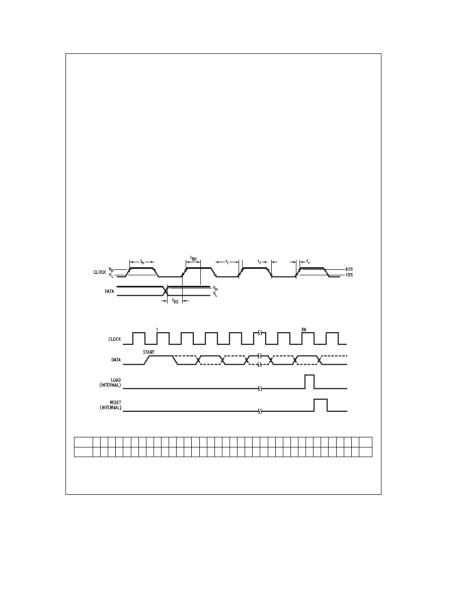
Figure 4 shows the input data format A start bit of logical
``1'' precedes the 35 bits of data At the 36th clock a LOAD
signal is generated synchronously with the high state of the
clock which loads the 35 bits of the shift registers into the
latches At the low state of the clock a RESET signal is
generated which clears all the shift registers for the next set
of data The shift registers are static master-slave configura-
tion There is no clear for the master portion of the first shift
register thus allowing continuous operation
There must be a complete set of 36 clocks or the shift regis-
ters will not clear
When the chip first powers ON an internal power ON reset
signal is generated which resets all registers and all latches
The START bit and the first clock return the chip to its nor-
mal operation
Figure 5 shows the Output Data Format for the 5480 Be-
cause it uses only 23 of the possible 35 outputs 12 of the
bits are `Don't Cares'
Figure 3 shows the timing relationships between data and
clock A maximum clock frequency of 0 5 MHz is assumed
For applications where a lesser number of outputs are used
it is possible to either increase the current per output or
operate the part at higher than 1V V
OUT
The following
equation can be used for calculations
T
j
e
(V
OUT
) (I
LED
) (No of segments) (i
JA
)
a
T
A
where
T
j
e
junction temperature 150 C max
V
OUT
e
the voltage at the LED driver outputs
I
LED
e
the LED current
i
JA
e
thermal coefficient of the package
T
A
e
ambient temperature
i
JA
(Socket Mount)
e
58 C W
i
JA
(Board Mount)
e
52 C W
TL F 6138 ≠ 3
FIGURE 3
TL F 6138 ≠ 4
FIGURE 4 Input Data Format
START 1 2 3 4 5 6 7 8 9 10 11 12 13 14 15 16 17 18 19 20 21 22 23 24 25 26 27 28 29 30 31 32 33 34 35 5451
START X 1 2 3 4 5 6 7 X X X 8 9 10 11 X X X X 12 13 14 15 16 17 X 18 X X 19 20 21 22 23 X 5480
FIGURE 5 Output Data Format
3

Functional Description
(Continued)
I
19
e
D
V
1k
TL F 6138 ≠ 5
FIGURE 6 Typical Application of Constant Current Brightness Control
TL F 6138 ≠ 6
FIGURE 7 Brightness Control Varying the Duty Cycle
Safe Operating Area
TL F 6138 ≠ 7
Basic 3
-Digit Interface
TL F 6138 ≠ 8
4

5