 | –≠–ª–µ–∫—Ç—Ä–æ–Ω–Ω—ã–π –∫–æ–º–ø–æ–Ω–µ–Ω—Ç: MM58341 | –°–∫–∞—á–∞—Ç—å:  PDF PDF  ZIP ZIP |
TL F 5603
MM58341
High
Voltage
Display
Driver
March 1991
MM58341 High Voltage Display Driver
General Description
The MM58341 is a monolithic MOS integrated circuit utiliz-
ing CMOS metal gate low threshold P and N-channel devic-
es It is available both in 40-pin molded dual-in-line pack-
ages or as dice The MM58341 is particularly suited for driv-
ing high voltage (35V max) vacuum fluorescent (VF) dis-
plays (e g a 32-digit alphanumeric or dot matrix display)
Applications
Y
COPS
TM
or microprocessor-driven displays
Y
Instrumentation readouts
Y
Industrial control indicator
Y
Digital clock thermostat counter voltmeter
Y
Word processor text displays
Y
Automotive dashboards
Features
Y
Direct interface to high voltage display
Y
Serial data input
Y
No external resistors required
Y
Wide display power supply operation
Y
LSTTL compatible inputs
Y
Software compatible with NS display driver family
Y
Compatible with alphanumeric or dot matrix displays
Y
Display blanking control input
Y
Simple to cascade
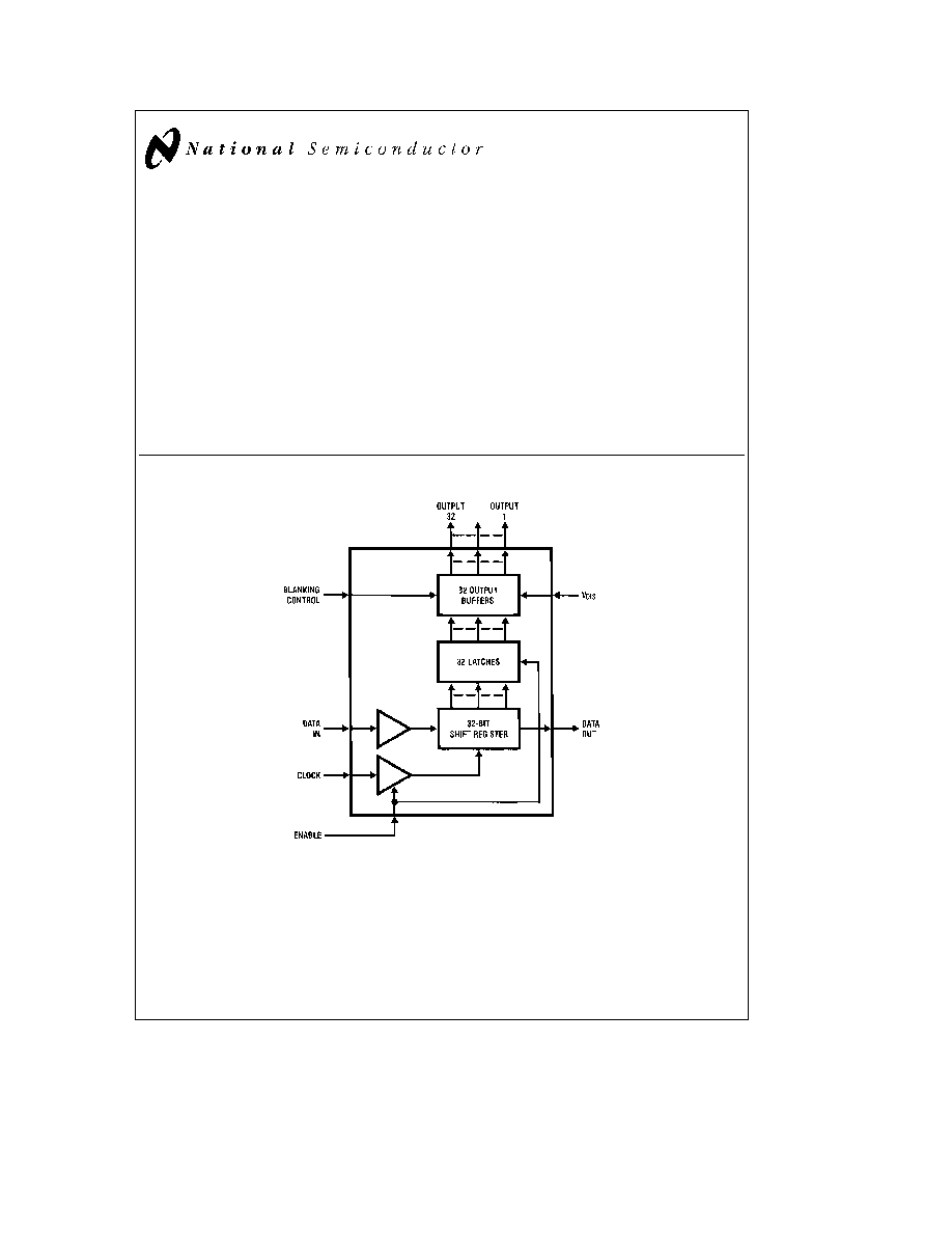
Block Diagram
TL F 5603 ≠ 1
FIGURE 1
COPS
TM
is a trademark of National Semiconductor Corp
C1995 National Semiconductor Corporation
RRD-B30M105 Printed in U S A

Absolute Maximum Ratings
If Military Aerospace specified devices are required
please contact the National Semiconductor Sales
Office Distributors for availability and specifications
Voltage at Any Input Pin
V
DD
a
0 3V to V
SS
b
0 3V
Voltage at Any Display Pin
V
DD
to V
DD
b
36 5V
V
DD
a
l
V
DIS
l
36 5V
Storage Temperature
b
65 C to
a
150 C
Power Dissipation at 25 C
Molded DIP Package Board Mount
2 28W
Molded DIP Package Socket Mount
2 05W
Molded DIP Package Board Mount
i
JA
e
46 C W
Derate 21 7 mW C Above 25 C
Molded DIP Package Socket Mount
i
JA
e
51 C W
Derate 19 6 mW C Above 25 C
Junction Temperature
130 C
Lead Temperature (Soldering 10 seconds)
260 C
Operating Conditions
Min
Max
Units
Supply Voltage (V
DD
)
V
SS
e
0V
4 5
5 5
V
Display Voltage (V
DIS
)
b
30
b
10
V
Temperature Range
b
40
a
85
C
DC Electrical Characteristics
T
A
e b
40 C to
a
85 C V
DD
e
5V
g
0 5V V
SS
e
0V unless otherwise specified
Symbol
Parameter
Conditions
Min
Typ
Max
Units
I
DD
Power Supply Currents
V
IN
e
V
SS
or V
DD
V
SS
e
0V
150
m
A
V
DIS
Disconnected
I
DIS
V
DD
e
5 5V V
SS
e
0V
10
mA
V
DIS
e b
30V All Outputs Low
V
IL
Input Logic Levels DATA IN
0 8
V
CLOCK ENABLE BLANK Logic `0'
V
IH
Input Logic Levels DATA IN
(Note 1)
2 4
V
CLOCK ENABLE BLANK Logic `1'
V
OH
Data Output Logic Levels
I
OUT
e
400 mA
0 4
V
Logic `0'
V
OH
Data Output Logic Levels
I
OUT
e b
10 mA
V
DD
b
0 5
V
Logic `1'
V
OH
Data Output Logic Levels
I
OUT
e b
500 mA
2 8
V
Logic `1'
I
IN
Input Currents DATA IN
V
IN
e
0V or V
DD
b
10
10
m
A
CLOCK ENABLE BLANK
C
IN
Input Capacitance DATA IN
15
pF
CLOCK ENABLE BLANK
R
OFF
Display Output Impedances
V
DD
e
5 5V V
SS
e
0V
Output Off
(Figure 3a)
V
DIS
e b
10V
55
250
kX
V
DIS
e b
20V
60
300
kX
V
DIS
e b
30V
65
400
kX
R
ON
Display Output Impedances
Output On
(Figure 3b)
V
DIS
e b
10V
700
800
X
V
DIS
e b
20V
600
750
X
V
DIS
e b
30V
500
680
X
V
DOL
Display Output Low Voltage
V
DD
e
5 5V I
OUT
e
Open Circuit
V
DIS
V
DIS
a
2
V
b
30V
s
V
DIS
s
b
10V
Note 1
74LSTTL V
OH
e
2 7V
I
OUT
e b
400 mA TTL V
OH
e
2 4V
I
OUT
e b
400 mA
2
AC Electrical Characteristics
T
A
e b
40 C to
a
85 C V
DD
e
5V
g
0 5V
Symbol
Parameter
Conditions
Min
Typ
Max
Units
f
C
Clock Input Frequency
(Notes 3 4)
800
kHz
t
H
Clock Input High Time
300
ns
t
L
Clock Input Low Time
300
ns
t
DS
Data Input Setup Time
100
ns
t
DH
Data Input Hold Time
100
ns
t
ES
Enable Input Setup Time
100
ns
t
EH
Enable Input Hold Time
100
ns
t
CDO
Data Output Clock Low to
C
L
e
50 pF
500
ns
Data Out Time
Note 2
Note that for timing purposes the signals ENABLE and BLANK can be considered to be totally independent of each other
Note 3
AC input waveform specification for test purpose t
r
s
20 ns t
f
s
20 ns f
e
800 kHz 50%
g
10% duty cycle
Note 4
Clock input rise and fall times must not exceed 5 ms
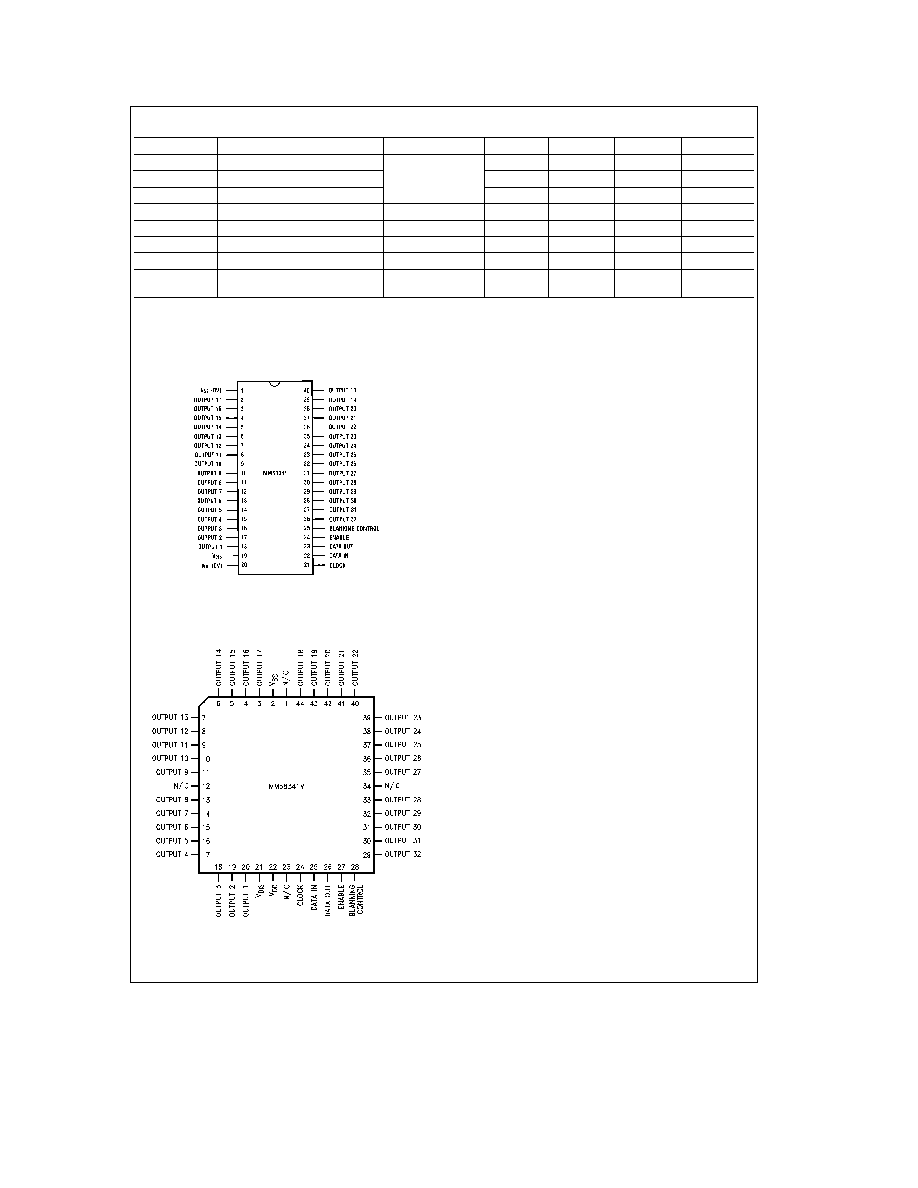
Connection Diagrams
Dual-In-Line Package
TL F 5603 ≠ 2
Top View
Order Number MM58341N
See NS Package Number N40A
Plastic Chip Carrier
TL F 5603 ≠ 8
Top View
Order Number MM58341V
See NS Package Number V44A
Functional Description
This product is specifically designed to drive multiplexed or
non-multiplexed high voltage alphanumeric or dot matrix
vacuum fluorescent (VF) displays Character generation is
done externally in the microprocessor with a serial data
path to the display driver The MM58341 uses three signals
DATA IN CLOCK and ENABLE where ENABLE acts as an
external load signal Display blanking can be achieved by
means of the BLANKING CONTROL input and a logic `1'
will turn off all sections of the display A block diagram of
the MM58341 is shown in
Figure 1
Figure 2 shows the pinout of the MM58341 device where
output 1 (pin 18) is equivalent to bit 1 (i e the first bit of data
to be loaded into the shift register following ENABLE high)
A logic `1' at the input will turn on the corresponding display
digit segment dot output
A significant reduction in discrete board components can be
achieved by use of the MM58341 because external pull-
down resistors are not required Due to the nature of the
output stage both its on and off impedance values vary as a
function of the display voltage applied However
Figures 3a
and
3b show that this output impedance will remain con-
stant for a fixed value of display voltage
Figure 4 demonstrates the critical timing requirements be-
tween CLOCK and DATA IN for the MM58341
To clear (reset) the display driver at power on or any time
the following flushing routine may be used With the enable
signal high clock in 32 zeroes Drive the enable signal low
and the display will be blank It is recommended to clear the
driver at power on
In
Figure 5 the ENABLE signal acts as an envelope and
only while this signal is at a logic `1' does the circuit accept
CLOCK input signals Data is transferred and shifted in the
internal shift register on the rising clock edge i e
`0' ≠ `1'
transition When the ENABLE signal goes low the contents
of the shift registers are latched and the display will show
new data During data transfer the display will show old
data DATA OUT is also provided on the MM58341 being
output on the falling edge At any time the display may be
blanked under processor control using the BLANKING
CONTROL input
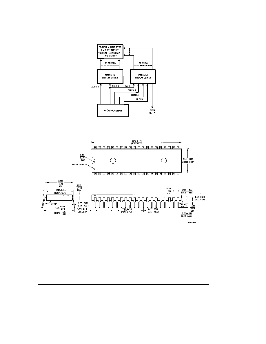
Figure 6 shows a schematic diagram of a microprocessor-
based system where the MM58341 is used to provide the
grid drive for a 32-digit 5 x 7 dot matrix vacuum fluorescent
(VF) display The anode drive in this example is provided by
another member of the high voltage display driver family
namely the MM58348 which does not require an externally
generated load signal
3

Functional Decription
(Continued)
TL F 5603 ≠ 3
FIGURE 3a Output Impedance Off
TL F 5603 ≠ 4
FIGURE 3b Output Impedance On
Timing Diagrams
TL F 5603 ≠ 5
For the purposes of AC measurements V
IH
e
2 4V V
IL
e
0 8V
FIGURE 4 Clock and Data Timings
TL F 5603 ≠ 6
FIGURE 5 MM58341 Timings (Data Format)
4
Typical Application
TL F 5603 ≠ 7
FIGURE 6 Microprocessor-Controlled Word Processor
Physical Dimensions
inches (millimeters)
Molded Dual-In-Line Package (N)
Order Number MM58341N
NS Package Number N40A
5