
TL F 5007
MM54HC147MM74HC147
10-to-4
Line
Priority
Encoder
November 1995
MM54HC147 MM74HC147
10-to-4 Line Priority Encoder
General Description
This high speed 10-to-4 Line Priority Encoder utilizes ad-
vanced silicon-gate CMOS technology It possesses the
high noise immunity and low power consumption of stan-
dard CMOS integrated circuits This device is fully buffered
giving it a fanout of 10 LS-TTL loads
The MM54HC147 MM74HC147 features priority encoding
of the inputs to ensure that only the highest order data line
is encoded Nine input lines are encoded to a four line BCD
output The implied decimal zero condition requires no input
condition as zero is encoded when all nine data lines are at
a high logic level All data inputs and outputs are active at
the low logic level
The 54HC 74HC logic family is functionally as well as pin-
out compatible with the standard 54LS 74LS logic family
All inputs are protected from damage due to static dis-
charge by internal diode clamps to V
CC
and ground
Features
Y
Low quiescent power consumption 40 mW maximum at
25 C
Y
High speed 31 ns propagation delay (typical)
Y
Low input current 1 mA maximum
Y
Wide supply range 2V to 6V
Connection and Logic Diagrams
Dual-In-Line Package
TL F 5007 � 1
Top View
Order Number MM54HC147 or MM74HC147
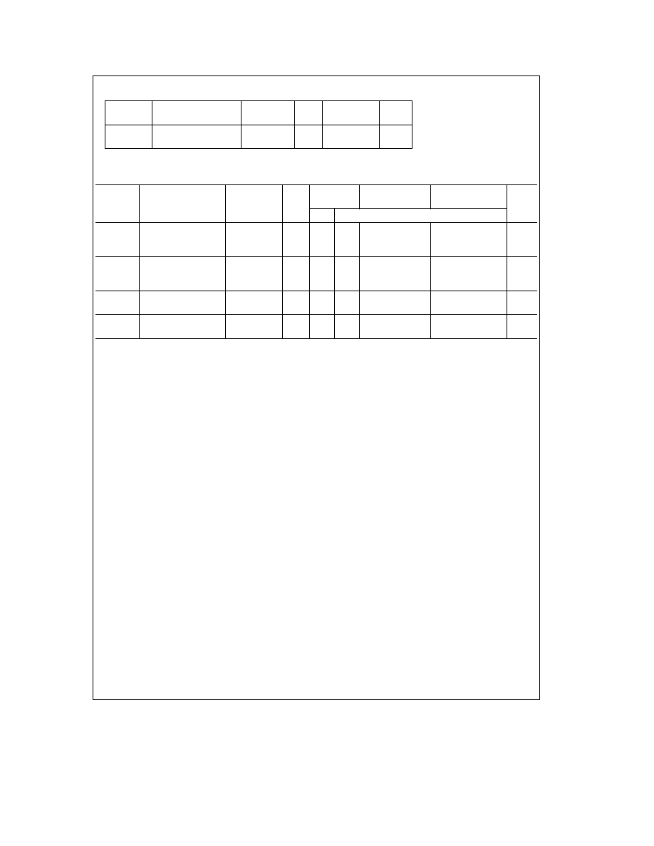
Truth Table
Inputs
Outputs
1
2
3
4
5
6
7
8
9
D
C
B
A
H
H
H
H
H
H
H
H
H
H
H
H
H
X
X
X
X
X
X
X
X
L
L
H
H
L
X
X
X
X
X
X
X
L
H
L
H
H
H
X
X
X
X
X
X
L
H
H
H
L
L
L
X
X
X
X
X
L
H
H
H
H
L
L
H
X
X
X
X
L
H
H
H
H
H
L
H
L
X
X
X
L
H
H
H
H
H
H
L
H
H
X
X
L
H
H
H
H
H
H
H
H
L
L
X
L
H
H
H
H
H
H
H
H
H
L
H
L
H
H
H
H
H
H
H
H
H
H
H
L
H
e
High Logic Level L
e
Low Logic Level X
e
Irrelevant
TL F 5007 � 2
C1995 National Semiconductor Corporation
RRD-B30M115 Printed in U S A

Absolute Maximum Ratings
(Notes 1
2)
If Military Aerospace specified devices are required
please contact the National Semiconductor Sales
Office Distributors for availability and specifications
Supply Voltage (V
CC
)
b
0 5 to
a
7 0V
DC Input Voltage (V
IN
)
b
1 5 to V
CC
a
1 5V
DC Output Voltage (V
OUT
)
b
0 5 to V
CC
a
0 5V
Clamp Diode Current (I
IK
I
OK
)
g
20 mA
DC Output Current per pin (I
OUT
)
g
25 mA
DC V
CC
or GND Current per pin (I
CC
)
g
50 mA
Storage Temperature Range (T
STG
)
b
65 C to
a
150 C
Power Dissipation (P
D
)
(Note 3)
600 mW
S O Package only
500 mW
Lead Temp (T
L
) (Soldering 10 seconds)
260 C
Operating Conditions
Min
Max
Units
Supply Voltage (V
CC
)
2
6
V
DC Input or Output Voltage
0
V
CC
V
(V
IN
V
OUT
)
Operating Temp Range (T
A
)
MM74HC
b
40
a
85
C
MM54HC
b
55
a
125
C
Input Rise or Fall Times
V
CC
e
2 0V
(t
r
t
f
)
1000
ns
V
CC
e
4 5V
500
ns
V
CC
e
6 0V
400
ns
DC Electrical Characteristics
(Note 4)
T
A
e
25 C
74HC
54HC
Symbol
Parameter
Conditions
V
CC
T
A
e b
40 to 85 C
T
A
e b
55 to 125 C
Units
Typ
Guaranteed Limits
V
IH
Minimum High Level
2 0V
1 5
1 5
1 5
V
Input Voltage
4 5V
3 15
3 15
3 15
V
6 0V
4 2
4 2
4 2
V
V
IL
Maximum Low Level
2 0V
0 5
0 5
0 5
V
Input Voltage
4 5V
1 35
1 35
1 35
V
6 0V
1 8
1 8
1 8
V
V
OH
Minimum High Level
V
IN
e
V
IH
or V
IL
Output Voltage
l
I
OUT
l
s
20 mA
2 0V
2 0
1 9
1 9
1 9
V
4 5V
4 5
4 4
4 4
4 4
V
6 0V
6 0
5 9
5 9
5 9
V
V
IN
e
V
IH
or V
IL
l
I
OUT
l
s
4 0 mA
4 5V
4 7
3 98
3 84
3 7
V
l
I
OUT
l
s
5 2 mA
6 0V
5 2
5 48
5 34
5 2
V
V
OL
Maximum Low Level
V
IN
e
V
IH
or V
IL
Output Voltage
l
I
OUT
l
s
20 mA
2 0V
0
0 1
0 1
0 1
V
4 5V
0
0 1
0 1
0 1
V
6 0V
0
0 1
0 1
0 1
V
V
IN
e
V
IH
or V
IL
l
I
OUT
l
s
4 0 mA
4 5V
0 2
0 26
0 33
0 4
V
l
I
OUT
l
s
5 2 mA
6 0V
0 2
0 26
0 33
0 4
V
I
IN
Maximum Input
V
IN
e
V
CC
or GND
6 0V
g
0 1
g
1 0
g
1 0
m
A
Current
I
CC
Maximum Quiescent
V
IN
e
V
CC
or GND
6 0V
8 0
80
160
m
A
Supply Current
I
OUT
e
0 mA
Note 1
Absolute Maximum Ratings are those values beyond which damage to the device may occur
Note 2
Unless otherwise specified all voltages are referenced to ground
Note 3
Power Dissipation temperature derating
plastic ``N'' package
b
12 mW C from 65 C to 85 C ceramic ``J'' package
b
12 mW C from 100 C to 125 C
Note 4
For a power supply of 5V
g
10% the worst case output voltages (V
OH
and V
OL
) occur for HC at 4 5V Thus the 4 5V values should be used when designing
with this supply Worst case V
IH
and V
IL
occur at V
CC
e
5 5V and 4 5V respectively (The V
IH
value at 5 5V is 3 85V ) The worst case leakage current (I
IN
I
CC
and
I
OZ
) occur for CMOS at the higher voltage and so the 6 0V values should be used
V
IL
limits are currently tested at 20% of V
CC
The above V
IL
specification (30% of V
CC
) will be implemented no later than Q1 CY'89
2
AC Electrical Characteristics
V
CC
e
5V T
A
e
25 C C
L
e
15 pF t
r
e
t
f
e
6 ns
Symbol
Parameter
Conditions
Typ
Guaranteed
Units
Limit
t
PHL
t
PLH
Maximum Propagation
31
38
ns
Delay
AC Electrical Characteristics
V
CC
e
2 0V to 6 0V C
L
e
50 pF t
r
e
t
f
e
6 ns (unless otherwise specified)
T
A
e
25 C
74HC
54HC
Symbol
Parameter
Conditions
V
CC
T
A
e b
40 to 85 C
T
A
e b
55 to 125 C
Units
Typ
Guaranteed Limits
t
PHL
t
PLH
Maximum Propagation
2 0V
181
220
275
319
ns
Delay
4 5V
36
44
55
64
ns
6 0V
31
37
47
54
ns
t
TLH
t
THL
Maximum Output Rise
2 0V
30
75
95
110
ns
and Fall Time
4 5V
8
15
19
22
ns
6 0V
7
13
16
19
ns
C
PD
Power Dissipation
(per package)
180
pF
Capacitance (Note 5)
C
IN
Maximum Input
5
10
10
10
pF
Capacitance
Note 5
C
PD
determines the no load dynamic power consumption P
D
e
C
PD
V
CC
2
f
a
I
CC
V
CC
and the no load dynamic current consumption I
S
e
C
PD
V
CC
f
a
I
CC
3
MM54HC147MM74HC147
10-to-4
Line
Priority
Encoder
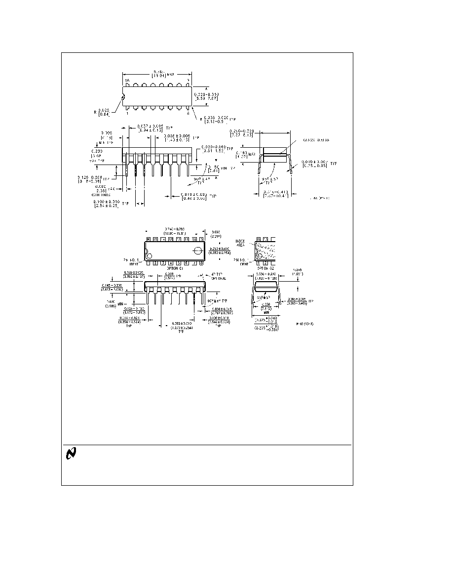
Physical Dimensions
inches (millimeters)
Order Number MM54HC147J or MM74HC147J
NS Package J16A
Order Number MM74HC147N
NS Package N16E
LIFE SUPPORT POLICY
NATIONAL'S PRODUCTS ARE NOT AUTHORIZED FOR USE AS CRITICAL COMPONENTS IN LIFE SUPPORT
DEVICES OR SYSTEMS WITHOUT THE EXPRESS WRITTEN APPROVAL OF THE PRESIDENT OF NATIONAL
SEMICONDUCTOR CORPORATION As used herein
1 Life support devices or systems are devices or
2 A critical component is any component of a life
systems which (a) are intended for surgical implant
support device or system whose failure to perform can
into the body or (b) support or sustain life and whose
be reasonably expected to cause the failure of the life
failure to perform when properly used in accordance
support device or system or to affect its safety or
with instructions for use provided in the labeling can
effectiveness
be reasonably expected to result in a significant injury
to the user
National Semiconductor
National Semiconductor
National Semiconductor
National Semiconductor
Corporation
Europe
Hong Kong Ltd
Japan Ltd
1111 West Bardin Road
Fax (a49) 0-180-530 85 86
13th Floor Straight Block
Tel 81-043-299-2309
Arlington TX 76017
Email cnjwge tevm2 nsc com
Ocean Centre 5 Canton Rd
Fax 81-043-299-2408
Tel 1(800) 272-9959
Deutsch Tel (a49) 0-180-530 85 85
Tsimshatsui Kowloon
Fax 1(800) 737-7018
English
Tel (a49) 0-180-532 78 32
Hong Kong
Fran ais Tel (a49) 0-180-532 93 58
Tel (852) 2737-1600
Italiano
Tel (a49) 0-180-534 16 80
Fax (852) 2736-9960
National does not assume any responsibility for use of any circuitry described no circuit patent licenses are implied and National reserves the right at any time without notice to change said circuitry and specifications