 | –≠–ª–µ–∫—Ç—Ä–æ–Ω–Ω—ã–π –∫–æ–º–ø–æ–Ω–µ–Ω—Ç: PC16552D | –°–∫–∞—á–∞—Ç—å:  PDF PDF  ZIP ZIP |

TL C 9426
PC16552D
Dual
Universal
Asynchronous
ReceiverTransmitter
with
FIFOs
June 1995
PC16552D
Dual Universal Asynchronous
Receiver Transmitter with FIFOs
General Description
The PC16552D is a dual version of the PC16550D Universal
Asynchronous Receiver Transmitter (UART) The two serial
channels are completely independent except for a common
CPU interface and crystal input On power-up both channels
are functionally identical to the 16450
Each channel can
operate with on-chip transmitter and receiver FIFOs (FIFO
mode) to relieve the CPU of excessive software overhead
In FIFO mode each channel is capable of buffering 16 bytes
(plus 3 bits of error data per byte in the RCVR FIFO) of data
in both the transmitter and receiver All the FIFO control
logic is on-chip to minimize system overhead and maximize
system efficiency
Signalling for DMA transfers is done through two pins per
channel (TXRDY and RXRDY) The RXRDY function is mul-
tiplexed on one pin with the OUT 2 and BAUDOUT func-
tions The CPU can select these functions through a new
register (Alternate Function Register)
Each channel performs serial-to-parallel conversion on data
characters received from a peripheral device or a MODEM
and parallel-to-serial conversion on data characters re-
ceived from the CPU The CPU can read the complete
status of each channel at any time Status information re-
ported includes the type and condition of the transfer opera-
tions being performed by the DUART as well as any error
conditions (parity overrun framing or break interrupt)
The DUART includes one programmable baud rate genera-
tor for each channel Each is capable of dividing the clock
input by divisors of 1 to (2
16
b
1) and producing a 16
c
clock for driving the internal transmitter logic Provisions are
also included to use this 16
c
clock to drive the receiver
logic The DUART has complete MODEM-control capability
and a processor-interrupt system Interrupts can be pro-
grammed to the user's requirements minimizing the com-
puting required to handle the communications link
The DUART is fabricated using National Semiconductor's
advanced M
2
CMOS
TM
Features
Y
Dual independent UARTs
Y
Capable of running all existing 16450 and PC16550D
software
Y
After reset all registers are identical to the 16450 reg-
ister set
Y
Read and write cycle times of 84 ns
Y
In the FIFO mode transmitter and receiver are each
buffered with 16-byte FIFOs to reduce the number of
interrupts presented to the CPU
Y
Holding and shift registers in the 16450 Mode eliminate
the need for precise synchronization between the CPU
and serial data
Y
Adds or deletes standard asynchronous communication
bits (start stop and parity) to or from the serial data
Y
Independently controlled transmit receive line status
and data set interrupts
Y
Programmable baud generators divide any input clock
by 1 to (2
16
b
1) and generate the 16
c
clock
Y
MODEM control functions (CTS RTS DSR DTR RI
and DCD)
Y
Fully programmable serial-interface characteristics
5- 6- 7- or 8-bit characters
Even odd or no-parity bit generation and detection
1- 1
- or 2-stop bit generation
Baud generation (DC to 1 5M baud) with 16
c
clock
Y
False start bit detection
Y
Complete status reporting capabilities
Y
TRI-STATE
TTL drive for the data and control buses
Y
Line break generation and detection
Y
Internal diagnostic capabilities
Loopback controls for communications link fault
isolation
Break parity overrun framing error simulation
Y
Full prioritized interrupt system controls
Can also be reset to 16450 Mode under software control
Note This part is patented
TRI-STATE
is a registered trademark of National Semiconductor Corporation
M
2
CMOS
TM
is a trademark of National Semiconductor Corporation
C1995 National Semiconductor Corporation
RRD-B30M75 Printed in U S A

Table of Contents
1 0 ABSOLUTE MAXIMUM RATINGS
2 0 DC ELECTRICAL CHARACTERISTICS
3 0 AC ELECTRICAL CHARACTERISTICS
4 0 TIMING WAVEFORMS
5 0 BLOCK DIAGRAM OF A SINGLE SERIAL CHANNEL
6 0 PIN DESCRIPTIONS
6 1 Input Signals
6 2 Output Signals
6 3 Input Output Signals
6 4 Clock Signals
6 5 Power
7 0 CONNECTION DIAGRAM
8 0 REGISTERS
8 1 Line Control Register
8 2 Typical Clock Circuits
8 0 REGISTERS
(Continued)
8 3 Programmable Baud Generator
8 4 Line Status Register
8 5 FIFO Control Register
8 6 Interrupt Identification Register
8 7 Interrupt Enable Register
8 8 Modem Control Register
8 9 Modem Status Register
8 10 Alternate Function Register
8 11 Scratchpad Register
9 0 FIFO Mode Operation
9 1 FIFO Interrupt Operation
9 2 FIFO Polled Operation
10 0 ORDERING INFORMATION
Basic Configuration
TL C 9426 ≠ 1
2
1 0 Absolute Maximum Ratings
Temperature under Bias
0 C to
a
70 C
Storage Temperature
b
65 C to
a
150 C
All Input or Output Voltages
with Respect to V
SS
b
0 5V to
a
7 0V
Power Dissipation
1W
Note
Maximum ratings indicate limits beyond which perma-
nent damage may occur Continuous operation at these lim-
its is not intended and should be limited to those conditions
specified under DC electrical characteristics
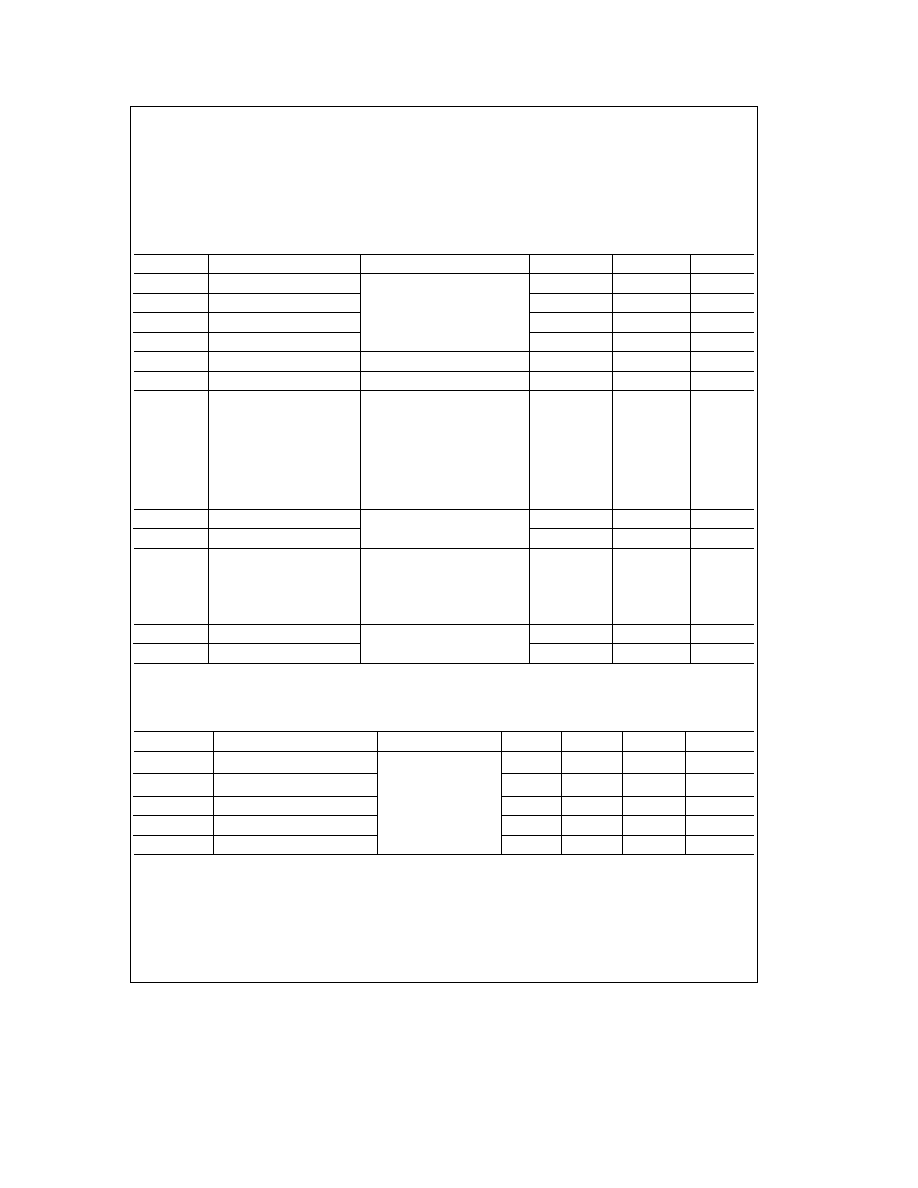
2 0 DC Electrical Characteristics
T
A
e
0 C to
a
70 C V
DD
e a
5V
g
10% V
SS
e
0V unless otherwise specified
Symbol
Parameter
Conditions
Min
Max
Units
V
ILX
Clock Input Low Voltage
b
0 5
0 8
V
V
IHX
Clock Input High Voltage
2
V
CC
V
V
IL
Input Low Voltage
b
0 5
0 8
V
V
IH
Input High Voltage
2
V
CC
V
V
OL
Output Low Voltage
I
OL
e
1 6 mA on all (Note 1)
0 4
V
V
OH
Output High Voltage
I
OH
e b
1 mA (Note 1)
2 4
V
I
CC
(AV)
Average Power Supply
V
DD
e
5 5V
Current
No Loads on Output
CS RD WR
SIN DSR DCD
30
mA
CTS RI
e
2V
All Other Inputs
e
0 8V
XIN
e
24 MHz
Divisor
e
EFFF
I
IL
Input Leakage
V
DD
e
5 5V V
SS
e
0V
g
10
m
A
I
CL
Clock Leakage
V
IN
e
0V 5 5V
g
10
m
A
I
OZ
TRI-STATE Leakage
V
DD
e
5 5V V
SS
e
0V
V
OUT
e
0V 5 5V
1) Chip Deselected
g
20
m
A
2) WRITE Mode
Chip Selected
V
ILMR
MR Schmitt V
IL
0 8
V
V
IHMR
MR Schmitt V
IH
2
V
Note 1
Does not apply to XOUT
Note 2
T
A
e
25 C
Capacitance
T
A
e
25 C V
DD
e
V
SS
e
0V
Symbol
Parameter
Conditions
Min
Typ
Max
Units
C
XIN
Clock Input Capacitance
7
9
pF
f
c
e
1 MHz
C
XOUT
Clock Output Capacitance
7
9
pF
Unmeasured Pins
C
IN
Input Capacitance
5
7
pF
Returned to V
SS
C
OUT
Output Capacitance
6
8
pF
C
I O
Input Output Capacitance
10
12
pF
3

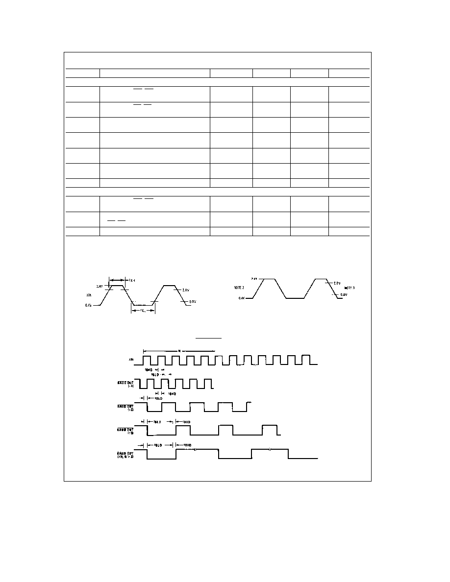
3 0 AC Electrical Characteristics
T
A
e
0 C to
a
70 C V
DD
e a
5V
g
10%
Symbol
Parameter
Conditions
Min
Max
Units
t
AR
RD Delay from Address
15
ns
t
AW
WR Delay from Address
15
ns
t
DH
Data Hold Time
5
ns
t
DS
Data Setup Time
15
ns
t
HZ
RD to Floating Data Delay
(Note 2)
10
20
ns
t
MR
Master Reset Pulse Width
500
ns
t
RA
Address Hold Time from RD
0
ns
t
RC
Read Cycle Update
29
ns
t
RD
RD Strobe Width
40
ns
t
RVD
Delay from RD to Data
25
ns
t
WA
Address Hold Time from WR
0
ns
t
WC
Write Cycle Update
29
ns
t
WR
WR Strobe Width
40
ns
t
XH
Duration of Clock High Pulse
External Clock (24 MHz Max)
17
ns
t
XL
Duration of Clock Low Pulse
External Clock (24 MHz Max)
17
ns
RC
Read Cycle
e
t
AR
a
t
RD
a
t
RC
84
ns
WC
Write Cycle
e
t
AW
a
t
WR
a
t
WC
84
ns
BAUD GENERATOR
N
Baud Divisor
1
2
16
b
1
t
BHD
Baud Output Positive Edge Delay
f
X
e
24 MHz
d
2
45
ns
t
BLD
Baud Output Negative Edge Delay
f
X
e
24 MHz
d
2
45
ns
RECEIVER
t
RAI
Delay from Active Edge of RD to
78
ns
Reset Interrupt
t
RINT
Delay from Inactive Edge of RD
(RD LSR)
40
ns
to Reset Interrupt
t
RXI
Delay from READ to RXRDY Inactive
55
ns
t
SCD
Delay from RCLK to Sample Time
33
ns
t
SINT
Delay from Stop to Set Interrupt
(Note 1)
2
BAUDOUT
Cycles
Note 1
In the FIFO mode (FCR0
e
1) the trigger level interrupts the receiver data available indication the active RXRDY indication and the overrun error
indication will be delayed 3 RCLKs Status indicators (PE FE BI) will be delayed 3 RCLKs after the first byte has been received For subsequently received bytes
these indicators will be updated immediately after RDRBR goes inactive Timeout interrupt is delayed 8 RCLKs
Note 2
Charge and discharge time is determined by V
OL
V
OH
and the external loading
Note 3
All AC timings can be met with current loads that don't exceed 3 2 mA or
b
80 mA at 100 pF capacitive loading
Note 4
For capacitive loads that exceed 100 pF the following typical derating factors should be used
100 pF
k
C
L
s
150 pF t
e
(0 1 ns pF)(C
L
b
100 pF)
150 pF
k
C
L
s
200 pF t
e
(0 08 ns pF)(C
L
b
100 pF)
I
SINK
t
e
(0 5 ns mA)(I
SINK
mA)
I
SOURCE
t
e
(0 5 ns mA)(I
SOURCE
mA)
Limits I
SOURCE
is negative I
SINK
s
4 8 mA I
SOURCE
s b
120 mA C
L
s
250 pF
AC Testing Load Circuit
TL C 9426 ≠ 22
4
3 0 AC Electrical Characteristics
T
A
e
0 C to
a
70 C V
DD
e a
5V
g
10% (Continued)
Symbol
Parameter
Conditions
Min
Max
Units
TRANSMITTER
t
HR
Delay from WR (WR THR)
40
ns
to Reset Interrupt
t
IR
Delay from RD (RD IIR) to Reset
40
ns
Interrupt (THRE)
t
IRS
Delay from Initial INTR Reset
8
24
BAUDOUT
to Transmit Start
Cycles
t
SI
Delay from Initial Write to Interrupt
(Note 1)
16
24
BAUDOUT
Cycles
t
STI
Delay from Start to Interrupt (THRE)
(Note 1)
8
BAUDOUT
Cycles
t
SXA
Delay from Start to TXRDY Active
8
BAUDOUT
Cycles
t
WXI
Delay from Write to TXRDY Inactive
25
ns
MODEM CONTROL
t
MDO
Delay from WR (WR MCR)
40
ns
to Output
t
RIM
Delay to Reset Interrupt from
78
ns
RD (RD MSR)
t
SIM
Delay to Set Interrupt from MODEM Input
40
ns
Note 1
This delay will be lengthened by 1 character time minus the last stop bit time if the transmitter interrupt delay circuit is active (See FIFO Interrupt Mode
Operation)
4 0 Timing Waveforms
All timings are referenced to valid 0 and valid 1
External Clock Input (24 MHz Max)
TL C 9426 ≠ 2
AC Test Points
TL C 9426 ≠ 3
Note 2
The 2 4V and 0 4V levels are the voltages that the inputs are driven to during AC testing
Note 3
The 2 0V and 0 8V levels are the voltages at which the timing tests are made
BAUDOUT Timing
TL C 9426 ≠ 4
5