Äîêóìåíòàöèÿ è îïèñàíèÿ www.docs.chipfind.ru
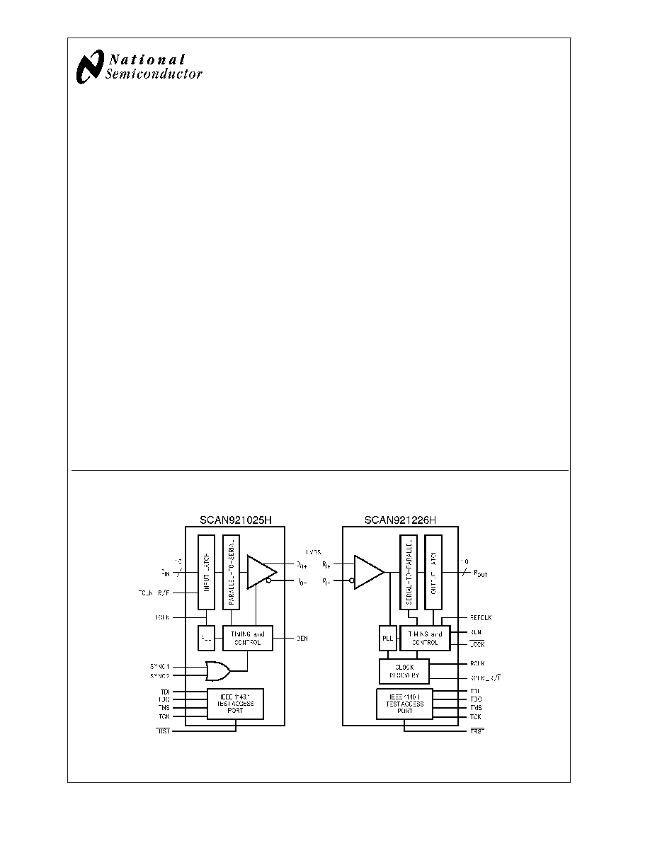
SCAN921025H and SCAN921226H
High Temperature 20-80 MHz 10 Bit Bus LVDS SerDes
with IEEE 1149.1 (JTAG) and at-speed BIST
General Description
The SCAN921025H transforms a 10-bit wide parallel
LVCMOS/LVTTL data bus into a single high speed Bus
LVDS serial data stream with embedded clock. The
SCAN921226H receives the Bus LVDS serial data stream
and transforms it back into a 10-bit wide parallel data bus
and recovers parallel clock.
Both devices are compliant with IEEE 1149.1 Standard for
Boundary Scan Test. IEEE 1149.1 features provide the de-
sign or test engineer access via a standard Test Access Port
(TAP) to the backplane or cable interconnects and the ability
to verify differential signal integrity. The pair of devices also
features an at-speed BIST mode which allows the intercon-
nects between the Serializer and Deserializer to be verified
at-speed.
The SCAN921025H transmits data over backplanes or
cable. The single differential pair data path makes PCB
design easier. In addition, the reduced cable, PCB trace
count, and connector size tremendously reduce cost. Since
one output transmits clock and data bits serially, it eliminates
clock-to-data and data-to-data skew. The powerdown pin
saves power by reducing supply current when not using
either device. Upon power up of the Serializer, you can
choose to activate synchronization mode or allow the Dese-
rializer to use the synchronization-to-random-data feature.
By using the synchronization mode, the Deserializer will
establish lock to a signal within specified lock times. In
addition, the embedded clock guarantees a transition on the
bus every 12-bit cycle. This eliminates transmission errors
due to charged cable conditions. Furthermore, you may put
the SCAN921025H output pins into TRI-STATE to achieve a
high impedance state. The PLL can lock to frequencies
between 20 MHz and 80 MHz.
Features
n
High Temperature Operation to 125°C
n
IEEE 1149.1 (JTAG) Compliant and At-Speed BIST test
mode.
n
Clock recovery from PLL lock to random data patterns.
n
Guaranteed transition every data transfer cycle
n
Chipset (Tx + Rx) power consumption
<
600 mW (typ)
@
80 MHz
n
Single differential pair eliminates multi-channel skew
n
800 Mbps serial Bus LVDS data rate (at 80 MHz clock)
n
10-bit parallel interface for 1 byte data plus 2 control bits
n
Synchronization mode and LOCK indicator
n
Programmable edge trigger on clock
n
High impedance on receiver inputs when power is off
n
Bus LVDS serial output rated for 27
load
n
Small 49-lead BGA package
Block Diagrams
20120701
October 2004
SCAN921025H
and
SCAN921226H
High
T
emperature
20-80
MHz
10
Bit
BL
VDS
SerDes
with
IEEE
1
149.1
(JT
AG)
and
at-speed
BIST
© 2004 National Semiconductor Corporation
DS201207
www.national.com
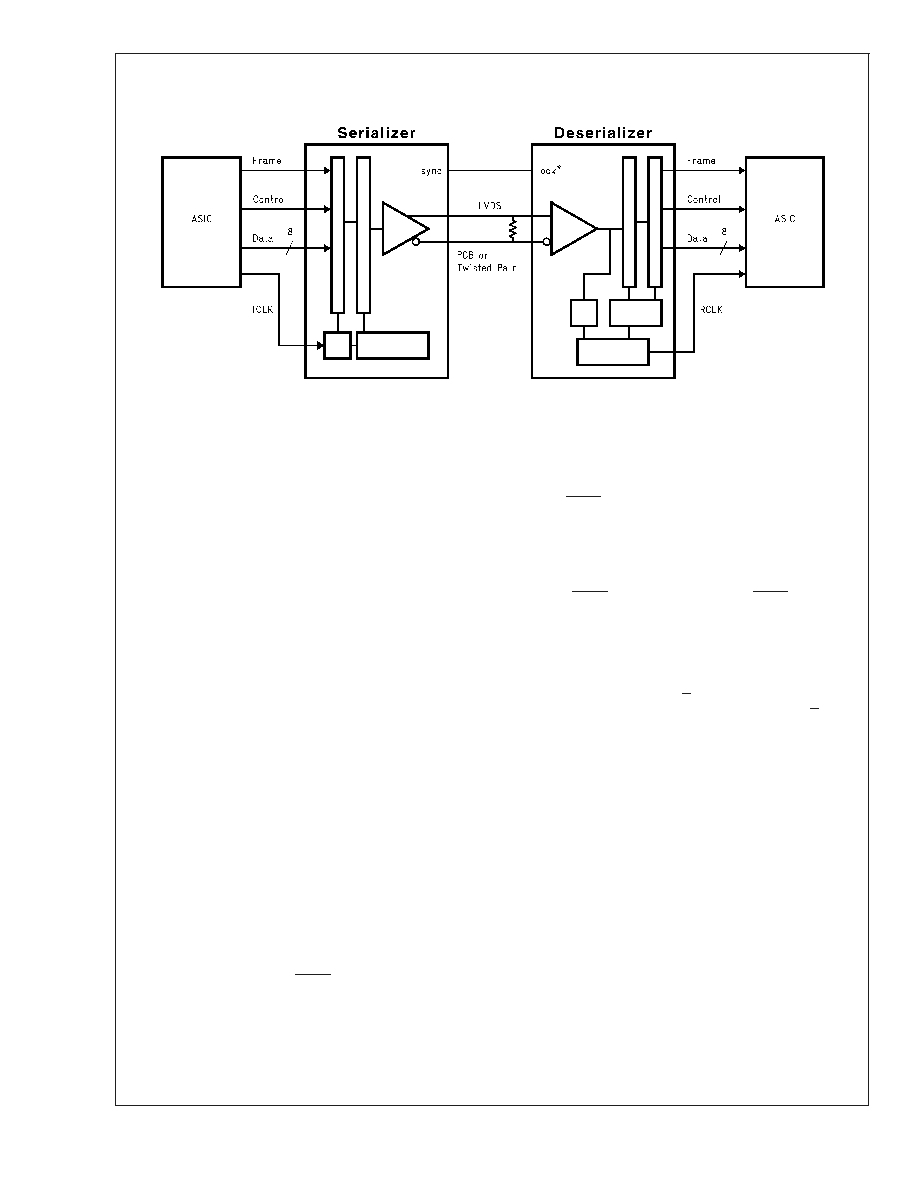
Block Diagrams
(Continued)
Application
20120702
Functional Description
The SCAN921025H and SCAN921226H are a 10-bit Serial-
izer and Deserializer chipset designed to transmit data over
differential backplanes at clock speeds from 20 to 80 MHz.
The chipset is also capable of driving data over Unshielded
Twisted Pair (UTP) cable.
The chipset has three active states of operation: Initializa-
tion, Data Transfer, and Resynchronization; and two passive
states: Powerdown and TRI-STATE. In addition to the active
and passive states, there are also test modes for JTAG
access and at-speed BIST.
The following sections describe each operation and passive
state and the test modes.
Initialization
Initialization of both devices must occur before data trans-
mission begins. Initialization refers to synchronization of the
Serializer and Deserializer PLL's to local clocks, which may
be the same or separate. Afterwards, synchronization of the
Deserializer to Serializer occurs.
Step 1: When you apply V
CC
to both Serializer and/or Dese-
rializer, the respective outputs enter TRI-STATE, and on-chip
power-on circuitry disables internal circuitry. When V
CC
reaches V
CC
OK (2.5V) the PLL in each device begins lock-
ing to a local clock. For the Serializer, the local clock is the
transmit clock (TCLK) provided by the source ASIC or other
device. For the Deserializer, you must apply a local clock to
the REFCLK pin.
The Serializer outputs remain in TRI-STATE while the PLL
locks to the TCLK. After locking to TCLK, the Serializer is
now ready to send data or SYNC patterns, depending on the
levels of the SYNC1 and SYNC2 inputs or a data stream.
The SYNC pattern sent by the Serializer consists of six ones
and six zeros switching at the input clock rate.
Note that the Deserializer LOCK output will remain high
while its PLL locks to the incoming data or to SYNC patterns
on the input.
Step 2: The Deserializer PLL must synchronize to the Seri-
alizer to complete initialization. The Deserializer will lock to
non-repetitive data patterns. However, the transmission of
SYNC patterns enables the Deserializer to lock to the Seri-
alizer signal within a specified time. See Figure 16.
The user's application determines control of the SYNC1 and
SYNC 2 pins. One recommendation is a direct feedback loop
from the LOCK pin. Under all circumstances, the Serializer
stops sending SYNC patterns after both SYNC inputs return
low.
When the Deserializer detects edge transitions at the Bus
LVDS input, it will attempt to lock to the embedded clock
information. When the Deserializer locks to the Bus LVDS
clock, the LOCK output will go low. When LOCK is low, the
Deserializer outputs represent incoming Bus LVDS data.
Data Transfer
After initialization, the Serializer will accept data from inputs
DIN0DIN9. The Serializer uses the TCLK input to latch
incoming Data. The TCLK_R/F pin selects which edge the
Serializer uses to strobe incoming data. TCLK_R/F high
selects the rising edge for clocking data and low selects the
falling edge. If either of the SYNC inputs is high for 5*TCLK
cycles, the data at DIN0-DIN9 is ignored regardless of clock
edge.
After determining which clock edge to use, a start and stop
bit, appended internally, frame the data bits in the register.
The start bit is always high and the stop bit is always low.
The start and stop bits function as the embedded clock bits
in the serial stream.
The Serializer transmits serialized data and clock bits (10+2
bits) from the serial data output (DO
±
) at 12 times the TCLK
frequency. For example, if TCLK is 80 MHz, the serial rate is
80 x 12 = 960 Mega-bits-per-second. Since only 10 bits are
from input data, the serial "payload" rate is 10 times the
TCLK frequency. For instance, if TCLK = 80 MHz, the pay-
load data rate is 80 x 10 = 800 Mbps. The data source
provides TCLK and must be in the range of 20 MHz to 80
MHz nominal.
The Serializer outputs (DO
±
) can drive a point-to-point con-
nection or in limited multi-point or multi-drop backplanes.
The outputs transmit data when the enable pin (DEN) is
SCAN921025H
and
SCAN921226H
www.national.com
2
Data Transfer
(Continued)
high, PWRDN = high, and SYNC1 and SYNC2 are low.
When DEN is driven low, the Serializer output pins will enter
TRI-STATE.
When the Deserializer synchronizes to the Serializer, the
LOCK pin is low. The Deserializer locks to the embedded
clock and uses it to recover the serialized data. ROUT data
is valid when LOCK is low. Otherwise ROUT0ROUT9 is
invalid.
The ROUT0-ROUT9 pins use the RCLK pin as the reference
to data. The polarity of the RCLK edge is controlled by the
RCLK_R/F input. See Figure 13.
ROUT(0-9), LOCK and RCLK outputs will drive a maximum
of three CMOS input gates (15 pF load) with a 80 MHz clock.
Resynchronization
When the Deserializer PLL locks to the embedded clock
edge, the Deserializer LOCK pin asserts a low. If the Dese-
rializer loses lock, the LOCK pin output will go high and the
outputs (including RCLK) will enter TRI-STATE.
The user's system monitors the LOCK pin to detect a loss of
synchronization. Upon detection, the system can arrange to
pulse the Serializer SYNC1 or SYNC2 pin to resynchronize.
Multiple resynchronization approaches are possible. One
recommendation is to provide a feedback loop using the
LOCK pin itself to control the sync request of the Serializer
(SYNC1 or SYNC2). Dual SYNC pins are provided for mul-
tiple control in a multi-drop application. Sending sync pat-
terns for resynchronization is desirable when lock times
within a specific time are critical. However, the Deserializer
can lock to random data, which is discussed in the next
section.
Random Lock Initialization and
Resynchronization
The initialization and resynchronization methods described
in their respective sections are the fastest ways to establish
the link between the Serializer and Deserializer. However,
the SCAN921226H can attain lock to a data stream without
requiring the Serializer to send special SYNC patterns. This
allows the SCAN921226H to operate in "open-loop" applica-
tions. Equally important is the Deserializer's ability to support
hot insertion into a running backplane. In the open loop or
hot insertion case, we assume the data stream is essentially
random. Therefore, because lock time varies due to data
stream characteristics, we cannot possibly predict exact lock
time. However, please see Table 1 for some general random
lock times under specific conditions. The primary constraint
on the "random" lock time is the initial phase relation be-
tween the incoming data and the REFCLK when the Dese-
rializer powers up. As described in the next paragraph, the
data contained in the data stream can also affect lock time.
If a specific pattern is repetitive, the Deserializer could enter
"false lock" - falsely recognizing the data pattern as the
clocking bits. We refer to such a pattern as a repetitive
multi-transition, RMT. This occurs when more than one Low-
High transition takes place in a clock cycle over multiple
cycles. This occurs when any bit, except DIN 9, is held at a
low state and the adjacent bit is held high, creating a 0-1
transition. In the worst case, the Deserializer could become
locked to the data pattern rather than the clock. Circuitry
within the SCAN921226H can detect that the possibility of
"false lock" exists. The circuitry accomplishes this by detect-
ing more than one potential position for clocking bits. Upon
detection, the circuitry will prevent the LOCK output from
becoming active until the potential "false lock" pattern
changes. The false lock detect circuitry expects the data will
eventually change, causing the Deserializer to lose lock to
the data pattern and then continue searching for clock bits in
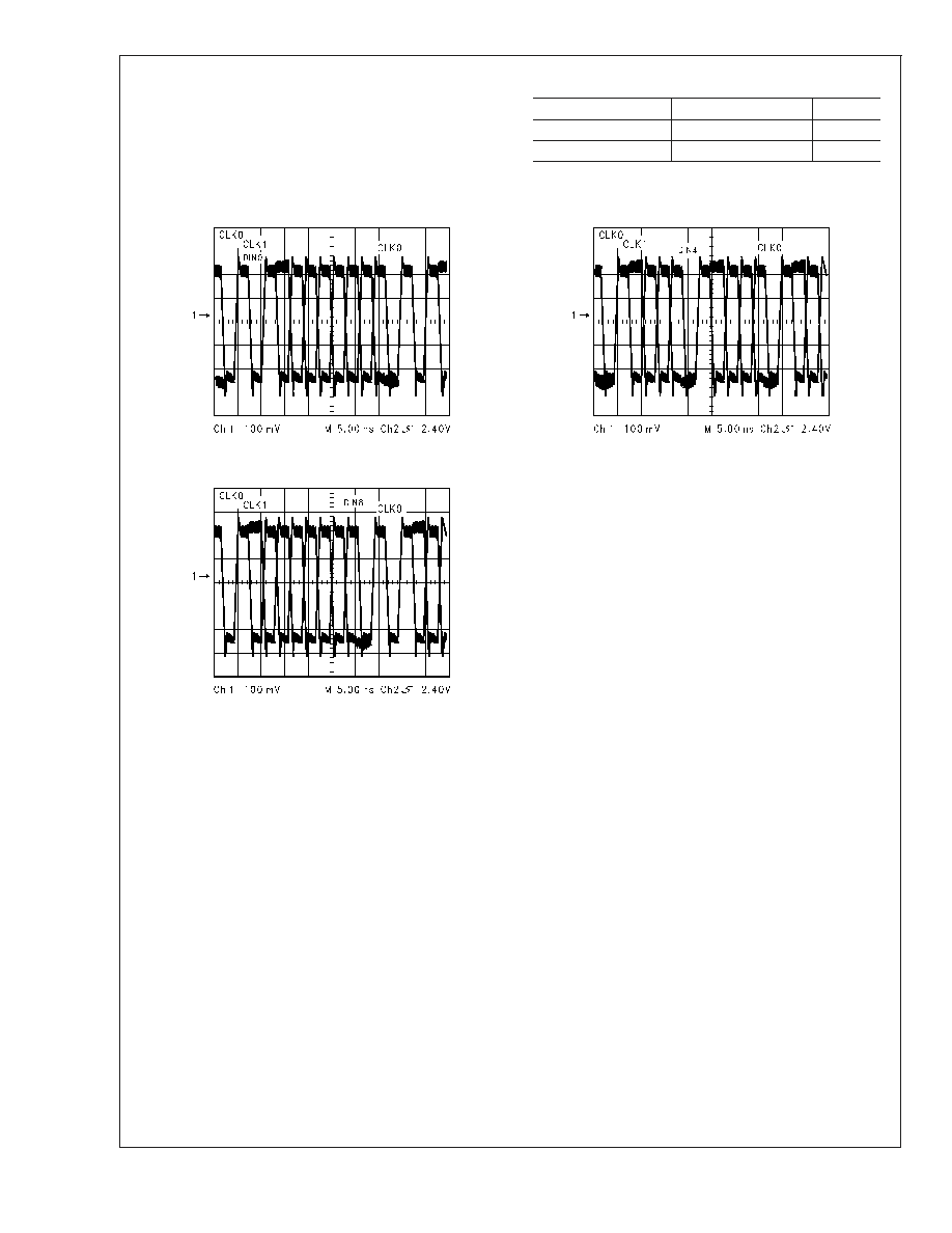
the serial data stream. Graphical representations of RMT are
shown in Figure 1. Please note that RMT only applies to bits
DIN0-DIN8.
Powerdown
When no data transfer occurs, you can use the Powerdown
state. The Serializer and Deserializer use the Powerdown
state, a low power sleep mode, to reduce power consump-
tion. The Deserializer enters Powerdown when you drive
PWRDN and REN low. The Serializer enters Powerdown
when you drive PWRDN low. In Powerdown, the PLL stops
and the outputs enter TRI-STATE, which disables load cur-
rent and reduces supply current to the milliampere range. To
exit Powerdown, you must drive the PWRDN pin high.
Before valid data exchanges between the Serializer and
Deserializer, you must reinitialize and resynchronize the de-
vices to each other. Initialization of the Serializer takes 510
TCLK cycles. The Deserializer will initialize and assert LOCK
high until lock to the Bus LVDS clock occurs.
TRI-STATE
The Serializer enters TRI-STATE when the DEN pin is driven
low. This puts both driver output pins (DO+ and DO-) into
TRI-STATE. When you drive DEN high, the Serializer returns
to the previous state, as long as all other control pins remain
static (SYNC1, SYNC2, PWRDN, TCLK_R/F).
When you drive the REN pin low, the Deserializer enters
TRI-STATE.
Consequently,
the
receiver
output
pins
(ROUT0ROUT9) and RCLK will enter TRI-STATE. The
LOCK output remains active, reflecting the state of the PLL.
TABLE 1.
Random Lock Times for the SCAN921226H
80 MHz
Units
Maximum
18
µs
Mean
3.0
µs
Minimum
0.43
µs
Conditions:
PRBS 2
15
, V
CC
= 3.3V
1) Difference in lock times are due to different starting points in the data
pattern with multiple parts.
Test Modes
In addition to the IEEE 1149.1 test access to the digital TTL
pins, the SCAN921025H and SCAN921226H have two in-
structions to test the LVDS interconnects. The first is EX-
TEST. This is implemented at LVDS levels and is only in-
tended as a go no-go test (e.g. missing cables). The second
method is the RUNBIST instruction. It is an "at-system-
speed" interconnect test. It is executed in approximately
28mS with a system clock speed of 80MHz. There are two
bits in the RX BIST data register for notification of PASS/
FAIL and TEST_COMPLETE. Pass indicates that the BER
(Bit-Error-Rate) is better than 10
-7
.
An important detail is that once both devices have the RUN-
BIST instruction loaded into their respective instruction reg-
isters, both devices must move into the RTI state within 4K
SCAN921025H
and
SCAN921226H
www.national.com
3
Test Modes
(Continued)
system clocks (At a SCLK of 66Mhz and TCK of 1MHz this
allows for 66 TCK cycles). This is not a concern when both
devices are on the same scan chain or LSP, however, it can
be a problem with some multi-drop devices. This test mode
has been simulated and verified using National's SCAN-
STA111.
Ordering Information
NSID
Function
Package
SCAN921025HSM
Serializer
SLC49a
SCAN921226HSM
Deserializer
SLC49a
20120724
DIN0 Held Low-DIN1 Held High Creates an RMT Pattern
20120725
DIN4 Held Low-DIN5 Held High Creates an RMT Pattern
20120726
DIN8 Held Low-DIN9 Held High Creates an RMT Pattern
FIGURE 1. RMT Patterns Seen on the Bus LVDS Serial Output
SCAN921025H
and
SCAN921226H
www.national.com
4
Absolute Maximum Ratings
(Note 1)
Supply Voltage (V
CC
)
-0.3V to +4V
LVCMOS/LVTTL Input Voltage
-0.3V to (V
CC
+0.3V)
LVCMOS/LVTTL Output Voltage
-0.3V to (V
CC
+0.3V)
Bus LVDS Receiver Input Voltage
-0.3V to +3.9V
Bus LVDS Driver Output Voltage
-0.3V to +3.9V
Bus LVDS Output Short Circuit
Duration
10mS
Junction Temperature
+150°C
Storage Temperature
-65°C to +150°C
Lead Temperature
(Soldering, 4 seconds)
+220°C
Maximum Package Power Dissipation Capacity
@
25°C Package:
49L BGA
1.47 W
Package Derating:
49L BGA
11.8 mW/°C above
+25°C
ja
85°C/W
ESD Rating
HBM
>
2kV
MM
>
250V
Recommended Operating
Conditions
Min
Nom
Max
Units
Supply Voltage (V
CC
)
3.0
3.3
3.6
V
Operating Free Air
Temperature (T
A
)
-40
+25
+125
°C
Receiver Input Range
0
2.4
V
Supply Noise Voltage
(V
CC
)
100
mV
P-P
Electrical Characteristics
Over recommended operating supply and temperature ranges unless otherwise specified.
Symbol
Parameter
Conditions
Min
Typ
Max
Units
SERIALIZER LVCMOS/LVTTL DC SPECIFICATIONS (apply to DIN0-9, TCLK, PWRDN, TCLK_R/F, SYNC1, SYNC2, DEN)
V
IH
High Level Input Voltage
2.0
V
CC
V
V
IL
Low Level Input Voltage
GND
0.8
V
V
CL
Input Clamp Voltage
I
CL
= -18 mA
-0.86
-1.5
V
I
IN
Input Current
V
IN
= 0V or 3.6V
-10
±
1
+10
µA
DESERIALIZER LVCMOS/LVTTL DC SPECIFICATIONS (apply to pins PWRDN, RCLK_R/ F, REN, REFCLK = inputs; apply
to pins ROUT, RCLK, LOCK = outputs)
V
IH
High Level Input Voltage
2.0
V
CC
V
V
IL
Low Level Input Voltage
GND
0.8
V
V
CL
Input Clamp Voltage
I
CL
= -18 mA
-0.62
-1.5
V
I
IN
Input Current
V
IN
= 0V or 3.6V
-10
±
1
+15
µA
V
OH
High Level Output Voltage
I
OH
= -9 mA
2.2
3.0
V
CC
V
V
OL
Low Level Output Voltage
I
OL
= 9 mA
GND
0.25
0.5
V
I
OS
Output Short Circuit Current
VOUT = 0V
-15
-47
-85
mA
I
OZ
TRI-STATE Output Current
PWRDN or REN = 0.8V, V
OUT
= 0V or VCC
-10
±
0.1
+10
µA
SERIALIZER Bus LVDS DC SPECIFICATIONS (apply to pins DO+ and DO-)
V
OD
Output Differential Voltage
(DO+)(DO-)
RL = 27
, Figure 17
200
290
mV
V
OD
Output Differential Voltage
Unbalance
35
mV
V
OS
Offset Voltage
1.05
1.1
1.3
V
V
OS
Offset Voltage Unbalance
4.8
35
mV
I
OS
Output Short Circuit Current
D0 = 0V, DIN = High,PWRDN and DEN =
2.4V
-56
-90
mA
I
OZ
TRI-STATE Output Current
PWRDN or DEN = 0.8V, DO = 0V or VCC
-10
±
1
+10
µA
I
OX
Power-Off Output Current
VCC = 0V, DO=0V or 3.6V
-20
±
1
+30
µA
SCAN921025H
and
SCAN921226H
www.national.com
5
Document Outline