 | –≠–ª–µ–∫—Ç—Ä–æ–Ω–Ω—ã–π –∫–æ–º–ø–æ–Ω–µ–Ω—Ç: ML674000 | –°–∫–∞—á–∞—Ç—å:  PDF PDF  ZIP ZIP |
OKI Semiconductor
FEDL674000-02
Issue Date: Dec. 10, 2002
ML674000
32-bit General-purpose, ARM-based Microcontroller
1/24
GENERAL DESCRIPTION
Oki's ML674000 standard microcontroller (MCU) is a member of an extensive and growing family of ARM
Æ
architecture 32-bit MCUs for general-purpose applications that require 32-bit CPU performance and low cost
afforded by MCU integrated features.
ML674000 MCU provides a host of useful peripherals such as 8KB of on-board SRAM, timers, watchdog timer,
pulse-width modulators, AD converter, UART's, GPIO connectivity capability, and external memory controller.
These integrated features make it ideal for embedded applications where low costs and low power consumption are
key.
Oki's ML674K series MCUs are capable of executing both the 32-bit ARM instruction set for high-performance
applications as well as the 16-bit Thumb
Æ
instruction set for power-efficient applications. With an ARM7TDMI
Æ
core operating at 33 MHz maximum frequency, ARM ThumbTM capabilities, and robust feature sets, the ML674K
series MCUs are suitable for an array of applications including high performance industrial controllers and
instrumentation, telecom, PC peripherals, security/surveillance, test equipment, and a variety of consumer
electronics devices.
The ARM7TDMI
Æ
Advantage
Oki's ML67 Family of low-cost ARM-based MCUs offers system designers a bridge from 8- and 16-bit
proprietary MCU architectures to ARM's higher-performance, affordable, widely-accepted industry standard
architecture and its industry-wide support infrastructure. The ARM industry infrastructure offers system
developers many advantages including software compatibility, many ready-to-use software applications, and
numerous choices among hardware and software development tools. These ARM-based advantages allow Oki's
customers to better leverage engineering resources, lower development costs, minimize project risks, and reduce
their product time to market. In addition, migration of a design with an Oki standard MCU to an Oki custom
solution is easily facilitated with its award-winning µPLATTM product development architecture.
FEATURES
∑ CPU
32-bit RISC CPU (ARM7TDMI)
32-bit instructions (ARM Instructions) and 16-bit instructions (Thumb Instructions) mixed
General purpose registers : 31 x 32 bits
Built-in Barrel shifter and multiplier (32 bit x 8 bit, Modified Booth's Algorithm)
Little endian
Built-in debug function
∑ Internal memory
RAM 8KB (32-bit access)
∑ External memory controller
ROM (FLASH): 16 Mbytes
SRAM: 16 Mbytes
DRAM: 64 Mbytes (SDRAM and EDO-DRAM support)
External IO devices: 16 Mbytes x 2 banks (with wait control by external signal)
ARM, ARM7TDMI, Multi-ICE and AMBA are registered trademarks of ARM Ltd., UK.
µPLAT is Oki's trademark.
The contents of this data sheet are subject to change for modification without notice.

FEDL674000-02
OKI Semiconductor
ML674000
2/24
∑ Interrupt controller
24 sources: 19 internals and 5 externals (IRQ: 4, FIQ: 1)
∑ DMA controller
2 channels: Dual address mode, cycle steal and burst tranfer mode
∑ Timer
1 channel: 16-bit auto reload for operating system
6 channels: 16-bit auto reload for application
1 channel: 16 bit watchdog timer
∑ Serial interface
1 channel: UART
1 channel: UART with 16-byte FIFO
∑ Parallel I/O Port
2 ports x 16 bits (bitwise input/output settings)
∑ PWM
2 channels x 16 bits
∑ Analog-to-Digital Converter
8 channels x 10 bits
∑ Power down mechanism
Standby (all clock stop) and Halt (clock stop by each function block)
Clock gear (selectable 1/1, 1/2, 1/4, 1/8, 1/16 input clock frequency)
∑ JTAG interface
Connectable to JTAG ICE (e.g. ARM MutiICE)
∑ Power supply voltage
Core section: 2.25 V to 2.75 V
IO section: 3.0 V to 3.6 V
∑ Operating frequency
33 MHz (Max.)
∑ Operating temperature (ambient temperature)
≠40∞C to +85∞C
∑ Package
128-pin plastic TQFP (P-TQFP128-1414-0.40-K)
144-pin plastic LFBGA (P-LFBGA144-1111-0.80)

FEDL674000-02
OKI Semiconductor
ML674000
3/24
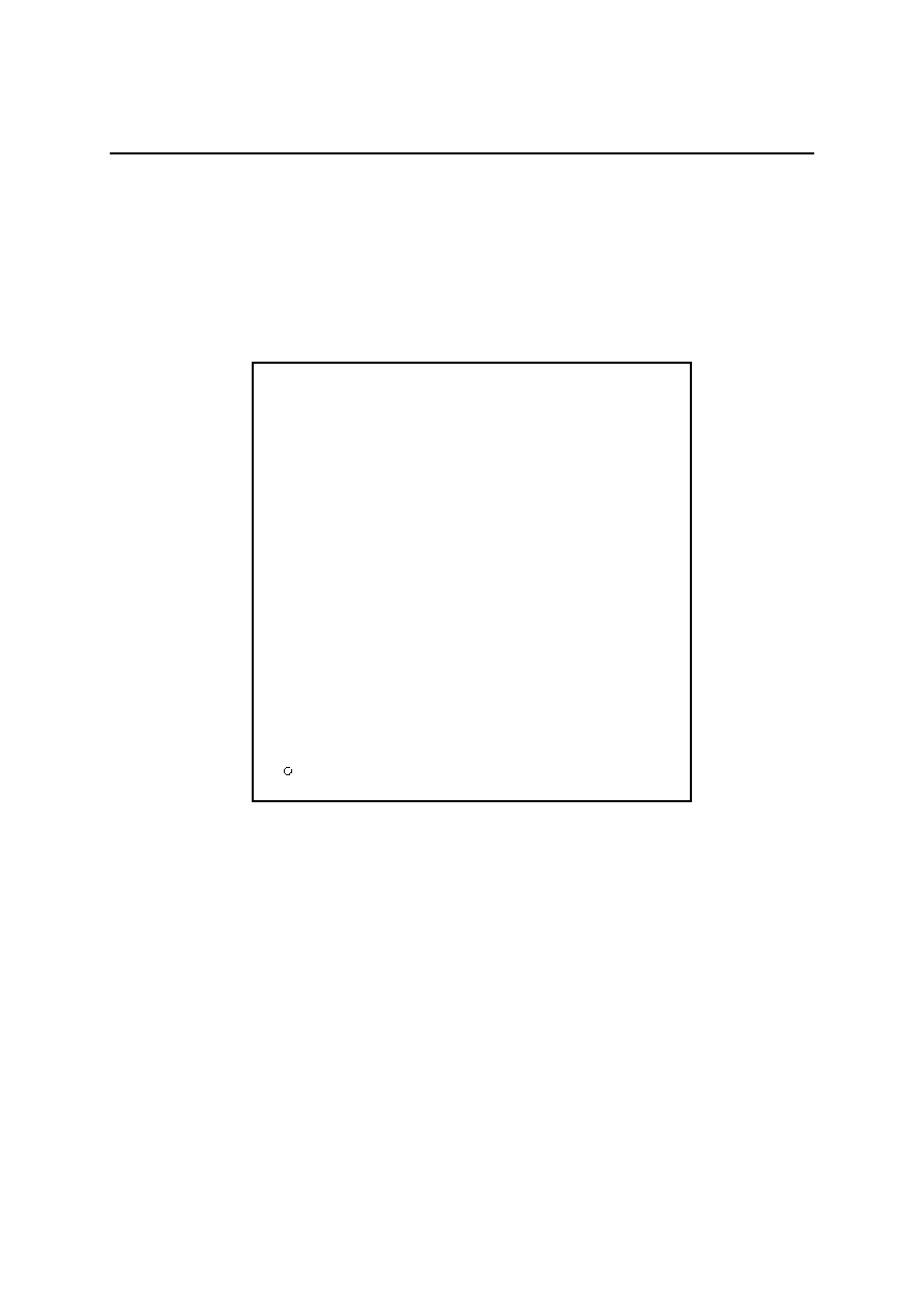
BLOCK DIAGRAM
TIC
Internal &
External
Memory
controller
IRC
AHB
Bridge
ARM7TDMI
APB
Bridge
SIO
System
Control
System
TMR
µPLAT-7B
CGB
APB
Bridge
WDT
UART
(16550)
PIOA[0]/SIN
PIOA[1]/SOUT
PIOA[2]/CTS
PIOA[3]/DSR
PIOA[4]/DCD
PIOA[5]/DTR
PIOA[6]/RTS
PIOA[7]/RI
AMBA
AHB bus
AMBA
APB bus
Ext.
IRC
APB bus
Internal RAM
8KB
TDI
TDO
nTRST
TMS
TCK
TBE
DBGRQ
DBGACK
TMR
16 bit x 6ch
8
8
PIOA[14:10]/XA[23:19]
XA[18:0]
XD[15:0]
PIOA[15]/XWR
XOE_N
XBWE_N[1:0]
XROMCS_N
XRAMCS_N
XIOCS_N[0]
XIOCS_N[1]
XBS_N[1:0]
PIOB[8]/XWAIT
PIOB[9]/XCAS_N
PIOB[10]/XRAS_N
PIOB[11]/XSDCLK
PIOB[12]/XSDCS_N
PIOB[13]/XSDCKE
PIOB[14]/
XDQM[1]/XCAS_N[1]
PIOB[15]/
XDQM[0]/XCAS_N[0]
A/D
AIN[7:0]
VREF
9
RESET_N
OSC0
OSC1_N
VDD_CORE
GND_CORE
VDD_IO
GND_IO
AVDD
AGND
MODE[2:0]
EFIQ_N
PWM
16 bit x 2ch
2
PIOB[7:6]/PWMOUT[1:0]
EXINT[3:0]
1
4
GPIO
32
DMAC
DRAMC
PIOA[15:0]
PIOB[15:0]
PIOA[8]/STXD
PIOA[9]/SRXD
PIOB[0]/DREQ[0]
PIOB[2]/DREQ[1]
PIOB[1]/DREQCLR[0]
PIOB[3]/DREQCLR[1]
PIOB[4:5]/TCOUT[1:0]
2
2
2
FEDL674000-02
OKI Semiconductor
ML674000
4/24
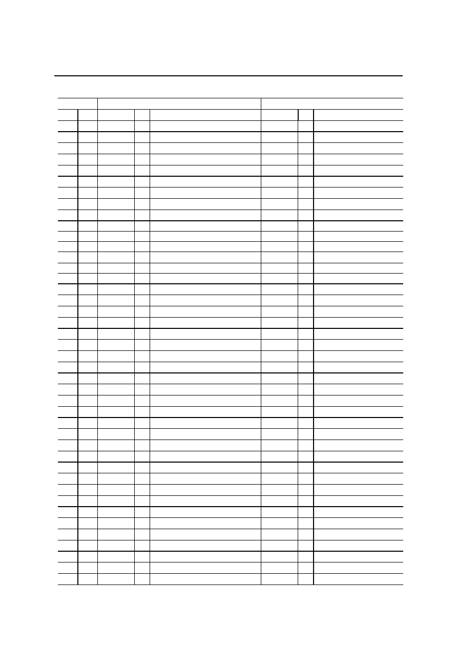
PIN CONFIGURATION (TOP VIEW)
(Primary
function)
PIOA[15]
XOE_N
XWE_N
XBWE_N[0]
XBWE_N[1]
XROMCS_N
XRAMCS_N
XIOCS_N[0]
XIOCS_N[1]
GND_CORE
VDD_CORE
PIOB[0]
PIOB[1]
VDD_IO
PIOB[2]
PIOB[3]
PIOB[4]
PIOB[5]
GND_IO
PIOB[6]
PIOB[7]
XBS_N[0]
XBS_N[1]
PIOB[8]
PIOB[9]
PIOB[10]
PIOB[11]
PIOB[12]
PIOB[13]
VDD_IO
(Secondary
function)
XWR
DREQ0
DREQCLR0
DREQ1
DREQCLR1
TCOUT0
TCOUT1
PWMOUT0
PWMOUT1
XWAIT
XCAS_N
XRAS_N
XSDCLK
XSDCS_N
XSDCKE
(P
ri
ma
ry
fu
nction
)
P
I
OA
[1
4]
P
I
OA
[1
3]
V
D
D_I
O
P
I
OA
[1
2]
P
I
OA
[1
1
]
P
I
OA
[1
0]
XA
[
1
8
]
XA
[
1
7
]
XA
[
1
6
]
XA
[
1
5
]
XA
[
1
4
]
XA
[
1
3
]
V
D
D_CORE
XA
[
1
2
]
XA
[
1
1
]
XA
[
1
0
]
XA
[
9
]
V
D
D_I
O
XA
[
8
]
XA
[
7
]
XA
[
6
]
XA
[
5
]
XA
[
4
]
XA
[
3
]
XA
[
2
]
XA
[
1
]
XA
[
0
]
XD
[
1
5
]
(S
e
c
on
da
r
y
fu
nction
)
XA
[
2
3
]
XA
[
2
2
]
XA
[
2
1
]
XA
[
2
0
]
XA
[
1
9
]
(Primary
function)
XD[14]
XD[13]
XD[12]
VDD_IO
XD[11]
XD[10]
XD[9]
XD[8]
GND_IO
XD[7]
XD[6]
XD[5]
XD[4]
XD[3]
XD[2]
XD[1]
XD[0]
VDD_CORE
OSC1_N
OSC0
GND_CORE
GND_IO
RESET_N
EFIQ_N
EXINT3
EXINT2
EXINT1
EXINT0
PIOA[9]
PIOA[8]
MODE[2]
MODE[1]
(Secondary
function)
SRXD
STXD
(P
ri
ma
ry
fu
ncti
on
)
PI
O
B
[
1
4
]
P
I
OB
[1
5]
DB
GRQ
DB
GACK
TD
I
TD
O
nT
RS
T
TM
S
TC
K
T
BE
P
I
OA
[0
]
P
I
OA
[1
]
P
I
OA
[2
]
P
I
OA
[3
]
P
I
OA
[4
]
P
I
OA
[5
]
P
I
OA
[6
]
P
I
OA
[7
]
V
DD_CORE
AV
D
D
VR
E
F
AI
N[
0
]
AI
N[
1
]
AI
N[
2
]
AI
N[
3
]
AI
N[
4
]
AI
N[
5
]
AI
N[
6
]
AI
N
[
7
]
M
O
DE
[0
]
(S
e
c
on
da
r
y
fu
nction
)
XD
Q
M
[
1
]
/
XC
AS
_
N
[
1
]
X
D
QM
[0]/XCA
S
_
N[
0]
SI
N
SO
UT
CT
S
DS
R
DCD
DT
R
RT
S
RI
97
98
99
100
101
102
103
104
105
106
107
108
109
110
111
112
113
114
115
116
117
118
119
120
121
122
123
124
125
126
127
128
96
95
94
93
92
91
90
89
88
87
86
85
84
83
82
81
80
79
78
77
76
75
74
73
72
71
70
69
68
67
66
65
64
63
62
61
60
59
58
57
56
55
54
53
52
51
50
49
48
47
46
45
44
43
42
41
40
39
38
37
36
35
34
33
1
2
3
4
5
6
7
8
9
10
11
12
13
14
15
16
17
18
19
20
21
22
23
24
25
26
27
28
29
30
31
32
GND_IO
GND_CORE
GND_IO
GND_IO
GND_IO
GND_IO
G
N
D_
C
O
RE
AG
ND
128-Pin Plastic TQFP

FEDL674000-02
OKI Semiconductor
ML674000
5/24
Note: Don't connect NC pins with others.
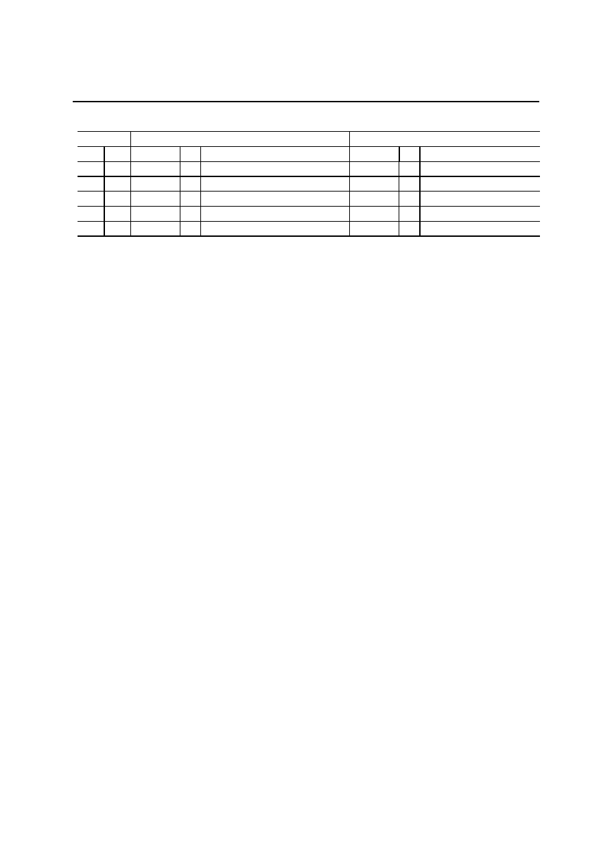
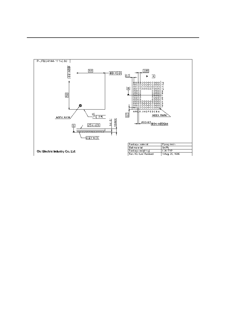
144-Pin Plastic LFBGA
A
B
C
D
E
F
G
H
J
K
L
M
N
13
NC
NC
NC
PIOA[12]/
XA[21]
XA[18]
XA[16]
GND_
CORE
XA[8]
XA[5]
XA[2]
GND_IO
XD[15]
NC
13
12
PIOA[15]/
XWR
PIOA[14]/
XA[23]
VDD_IO
GND_IO
XA[15]
XA[14]
XA[10]
GND_IO
XA[7]
XA[4]
XA[1]
NC
XD[14]
12
11
XOE_N
GND_IO
NC
PIOA[11]/
XA[20]
PIOA[10]/
XA[19]
VDD_
CORE
XA[12]
XA[9]
XA[3]
XA[0]
NC
VDD_IO
XD[13]
11
10
XBWE_
N[0]
XROM
CS_N
XWE_N
PIOA[13]/
XA[22]
XA[17]
XA[13]
XA[11]
VDD_IO
XA[6]
XD[12]
XD[10]
GND_IO
XD[11]
10
9
XRAM
CS_N
XIOCS_
N[1]
XBWE_
N[1]
XIOCS_
N[0]
XD[7]
XD[9]
XD[5]
XD[8]
9
8
GND_
CORE
VDD_
CORE
PIOB[1]/
DREQCLR
0
PIOB[0]/
DREQ0
XD[3]
XD[2]
XD[4]
XD[6]
8
7
PIOB[4]/
TCOUT0
VDD_IO
PIOB[3]/
DREQCLR
1
PIOB[2]/
DREQ1
XD[0]
XD[1]
NC
NC
7
6
XBS_N[0]
PIOB[6]/
PWMOUT0
PIOB[5]/
TCOUT1
GND_IO
NC
VDD_
CORE
OSC1_N
OSC0
6
5
PIOB[9]/
XCAS_N
PIOB[7]/
PWMOUT
1
PIOB[10]/
XRAS_N
XBS_N[1]
GND_IO
EXINT3
GND_
CORE
RESET_N
5
4
PIOB[12]/
XSDCS_N
PIOB[8]/
XWAIT
PIOB[11]/
XSDCLK
VDD_IO
TCK
PIOA[2]/
CTS
PIOA[5]/
DTR
VDD_
CORE
AIN[0]
AIN[7]
EXINT0
EFIQ_N
EXINT2
4
3
NC
PIOB[13]/
XSDCKE
NC
DBGRQ
TDO
PIOA[3]/
DSR
PIOA[6]/
RTS
GND_
CORE
AIN[3]
AIN[4]
PIOA[8]/
STXD
EXINT1
PIOA[9]/
SRXD
3
2
NC
GND_IO
DBGACK
nTRST
TBE
PIOA[1]/
SOUT
PIOA[4]/
DCD
NC
AVDD
AIN[1]
AIN[6]
NC
MODE[2]
2
1
NC
PIOB[14]/
XDQM[1]/
XCAS_N[1]
PIOB[15]/
XDQM[0]/
XCAS_N[0]
TDI
TMS
PIOA[0]/
SIN
PIOA[7]/
RI
VREF
AIN[2]
AIN[5]
AGND
MODE[0]
MODE[1]
1
A
B
C
D
E
F
G
H
J
K
L
M
N

FEDL674000-02
OKI Semiconductor
ML674000
6/24
LIST OF PINS
Pin Number
Primary Function
Secondary Function
TQFP LFBGA
Pin Name I/O
Function
Pin Name I/O
Function
1 B1 PIOB[14]
I/O
General-purpose
port (with interrupt function)
XDQM[1]/
XCAS_N[1]
O I/O mask/CAS (MSB)
2 C1 PIOB[15]
I/O
General-purpose
port (with interrupt function)
XDQM[0]/
XCAS_N[0]
O I/O mask/CAS (LSB)
3
D3
DBGRQ
I
Debugging input signal
-- --
4
C2
DBGACK
O Debugging output signal
-- --
5
D1
TDI
I
JTAG data input
-- --
6
E3
TDO
O JTAG data output
-- --
7 D2 nTRST I
JTAG
reset
-- --
8
E1
TMS
I
JTAG mode select
-- --
9 E4 TCK I
JTAG
clock
-- --
10
E2
TBE
I
Test input signal
-- --
11
F1
PIOA[0]
I/O General-purpose port (with interrupt function)
SIN
I
UART Serial Data In
12
F2
PIOA[1]
I/O General-purpose port (with interrupt function)
SOUT
O UART Serial Data Out
13
F4
PIOA[2]
I/O General-purpose port (with interrupt function)
CTS
I
UART Clear To Send
14
F3
PIOA[3]
I/O General-purpose port (with interrupt function)
DSR
I
UART Set Ready
15
G2
PIOA[4]
I/O General-purpose port (with interrupt function)
DCD
I
UART Carrier Detect
16
G4
PIOA[5]
I/O General-purpose port (with interrupt function)
DTR
O UART Data Terminal Ready
17
G3
PIOA[6]
I/O General-purpose port (with interrupt function)
RTS
O UART Request To Send
18
G1
PIOA[7]
I/O General-purpose port (with interrupt function)
RI
I
UART Ring Indicator
19 H3
GND_CORE
GND
Core
ground
-- --
20
H4
VDD_CORE VDD Core power supply
-- --
21
J2
AVDD
VDD Analog-to-digital converter power supply
-- --
22
H1
VREF
I
Analog-to-digital converter reference voltage
-- --
23
J4 AIN[0] I
Analog-to-digital converter analog input
-- --
24 K2 AIN[1] I
Analog-to-digital converter analog input
-- --
25
J1 AIN[2] I
Analog-to-digital converter analog input
-- --
26
J3 AIN[3] I
Analog-to-digital converter analog input
-- --
27 K3 AIN[4] I
Analog-to-digital converter analog input
-- --
28 K1 AIN[5] I
Analog-to-digital converter analog input
-- --
29 L2 AIN[6] I
Analog-to-digital converter analog input
-- --
30 K4 AIN[7] I
Analog-to-digital converter analog input
-- --
31
L1
AGND
GND GND for A/D converter
-- --
32 M1 MODE[0] I
Mode
setting
-- --
33 N1 MODE[1] I
Mode
setting
-- --
34 N2 MODE[2] I
Mode
setting
-- --
35
L3
PIOA[8]
I/O General-purpose port (with interrupt function)
STXD
O SIO transmit data output
36
N3
PIOA[9]
I/O General-purpose port (with interrupt function)
SRXD
I
SIO receive data input
37 L4 EXINT0 I
Interrupt
input
-- --
38 M3 EXINT1 I
Interrupt
input
-- --
39 N4 EXINT2 I
Interrupt
input
-- --

FEDL674000-02
OKI Semiconductor
ML674000
7/24
Pin Number
Primary Function
Secondary Function
TQFP LFBGA
Pin Name I/O
Function
Pin Name I/O
Function
40 L5 EXINT3 I
Interrupt
input
-- --
41 M4 EFIQ_N I
FIQ
input
-- --
42 N5 RESET_N I
Reset
input
-- --
43 K5 GND_IO
GND
I/O
ground
-- --
44 M5
GND_CORE
GND
Core
ground
-- --
45 N6 OSC0 I
Oscillator
input
-- --
46 M6 OSC1_N O
Oscillator
output
-- --
47
L6
VDD_CORE VDD Core power supply
-- --
48
K7
XD[0]
I/O External data bus
-- --
49
L7
XD[1]
I/O External data bus
-- --
50
L8
XD[2]
I/O External data bus
-- --
51
K8
XD[3]
I/O External data bus
-- --
52
M8
XD[4]
I/O External data bus
-- --
53
M9
XD[5]
I/O External data bus
-- --
54
N8
XD[6]
I/O External data bus
-- --
55
K9
XD[7]
I/O External data bus
-- --
56 M10 GND_IO GND
I/O
ground
-- --
57
N9
XD[8]
I/O External data bus
-- --
58
L9
XD[9]
I/O External data bus
-- --
59
L10
XD[10]
I/O External data bus
-- --
60
N10
XD[11]
I/O External data bus
-- --
61
M11
VDD_IO
VDD I/O power supply
-- --
62
K10
XD[12]
I/O External data bus
-- --
63
N11
XD[13]
I/O External data bus
-- --
64
N12
XD[14]
I/O External data bus
-- --
65
M13
XD[15]
I/O External data bus
-- --
66 L13 GND_IO GND
I/O
ground
-- --
67
K11
XA[0]
O External address output
-- --
68
L12
XA[1]
O External address output
-- --
69
K13
XA[2]
O External address output
-- --
70
J11
XA[3]
O External address output
-- --
71
K12
XA[4]
O External address output
-- --
72
J13
XA[5]
O External address output
-- --
73
J10
XA[6]
O External address output
-- --
74
J12
XA[7]
O External address output
-- --
75
H13
XA[8]
O External address output
-- --
76 H12 GND_IO GND
I/O
ground
-- --
77
H10
VDD_IO
VDD I/O power supply
-- --
78
H11
XA[9]
O External address output
-- --
79
G12
XA[10]
O External address output
-- --
80
G10
XA[11]
O External address output
-- --
81
G11
XA[12]
O External address output
-- --
FEDL674000-02
OKI Semiconductor
ML674000
8/24
Pin Number
Primary Function
Secondary Function
TQFP LFBGA
Pin Name I/O
Function
Pin Name I/O
Function
82 G13
GND_CORE
GND
Core
ground
-- --
83
F11
VDD_CORE VDD Core power supply
-- --
84
F10
XA[13]
O External address output
-- --
85
F12
XA[14]
O External address output
-- --
86
E12
XA[15]
O External address output
-- --
87
F13
XA[16]
O External address output
-- --
88
E10
XA[17]
O External address output
-- --
89 D12 GND_IO GND
I/O
ground
-- --
90
E13
XA[18]
O External address output
-- --
91
E11
PIOA[10]
I/O General-purpose port (with interrupt function)
XA[19]
O External address output
92
D11
PIOA[11]
I/O General-purpose port (with interrupt function)
XA[20]
O External address output
93
D13
PIOA[12]
I/O General-purpose port (with interrupt function)
XA[21]
O External address output
94
C12
VDD_IO
VDD I/O power supply
-- --
95
D10
PIOA[13]
I/O General-purpose port (with interrupt function)
XA[22]
O External address output
96
B12
PIOA[14]
I/O General-purpose port (with interrupt function)
XA[23]
O External address output
97 A12 PIOA[15] I/O
General-purpose
port (with interrupt function)
XWR
O External bus data transfer direction
98
A11
XOE_N
O Output enable (except SDRAM)
-- --
99 C10 XWE_N O
Write
enable
-- --
100 B11 GND_IO GND
I/O
ground
-- --
101 A10 XBWE_N[0] O Write enable (LSB)
102
C9
XBWE_N[1]
O Write enable (MSB)
-- --
103
B10
XROMCS_N
O External ROM chip select
-- --
104
A9
XRAMCS_N
O External RAM chip select
-- --
105
D9
XIOCS_N[0]
O I/O bank 0 chip select
-- --
106
B9
XIOCS_N[1]
O I/O bank 1 chip select
-- --
107 A8 GND_CORE
GND
Core
ground
-- --
108
B8
VDD_CORE VDD Core power supply
-- --
109
D8
PIOB[0]
I/O General-purpose port (with interrupt function)
DREQ0
I
DMA request signal (Ch 0)
110
C8
PIOB[1]
I/O General-purpose port (with interrupt function) DREQCLR0
O DREQ clear signal (Ch 0)
111
B7
VDD_IO
VDD I/O power supply
-- --
112
D7
PIOB[2]
I/O General-purpose port (with interrupt function)
DREQ1
I
DMA request signal (Ch 1)
113
C7
PIOB[3]
I/O General-purpose port (with interrupt function) DREQCLR1
O DREQ clear signal (Ch 1)
114
A7
PIOB[4]
I/O General-purpose port (with interrupt function) TCOUT0 O
DMA
Termination Signal (CH 0)
115
C6
PIOB[5]
I/O General-purpose port (with interrupt function) TCOUT1 O
DMA
Termination Signal (CH 1)
116 D6 GND_IO GND
I/O
ground
-- --
117
B6
PIOB[6]
I/O General-purpose port (with interrupt function) PWMOUT0
O PWM output (Ch 0)
118
B5
PIOB[7]
I/O General-purpose port (with interrupt function) PWMOUT1
O PWM output (Ch 1)
119
A6
XBS_N[0]
O External bus byte select (LSB)
-- --
120
D5
XBS_N[1]
O External bus byte select (MSB)
-- --
121
B4
PIOB[8]
I/O General-purpose port (with interrupt function)
XWAIT
I
WAIT input for IO bank 0
122
A5
PIOB[9]
I/O General-purpose port (with interrupt function)
XCAS_N
O Column address strobe (SDRAM)
123
C5
PIOB[10]
I/O General-purpose port (with interrupt function)
XRAS_N
O Row address strobe (SDRAM/EDO)
FEDL674000-02
OKI Semiconductor
ML674000
9/24
Pin Number
Primary Function
Secondary Function
TQFP LFBGA
Pin Name I/O
Function
Pin Name I/O
Function
124
C4
PIOB[11]
I/O General-purpose port (with interrupt function)
XSDCLK
O SDRAM clock
125
A4
PIOB[12]
I/O General-purpose port (with interrupt function)
XSDCS_N
O SDRAM chip select
126
B3
PIOB[13]
I/O General-purpose port (with interrupt function)
XSDCKE
O Clock enable (SDRAM)
127
D4
VDD_IO
VDD I/O power supply
-- --
128 B2 GND_IO
GND I/O ground
-- --
Note: A1, C3, H2, M2, K6, M7, N7, M12, N13, L11, C13, B13, A13, C11, A3, A2 pins of LFBGA packaged
version are NC pins. These pins must be left unconnected.
FEDL674000-02
OKI Semiconductor
ML674000
10/24
PIN DESCRIPTION
Pin Name
I/O
Description
Primary/
Secondary
Logic
System
RESET_N I
Reset
input
--
Negative
OSC0 I
Crystal oscillator connection or external clock input.
Connect a crystal oscillator (16 MHz to 33 MHz), if used, to OSC0 and
OSC1_N.
--
OSC1_N O
Crystal oscillator connection.
Leave this pin unconnected if using external clock input.
--
TBE
I
Test pin. Drive at High level.
--
Negative
Debugging support.
DBGRQ
I
Debugging pin. Normally connect to ground.
--
Positive
DBGACK
O
Debugging pin. Normally leave open.
--
Positive
TCK
I
Debugging pin. Normally connect to ground.
--
--
TMS
I
Debugging pin. Normally drive at High level.
--
Positive
nTRST
I
Debugging pin. Normally connect to ground.
--
Negative
TDI
I
Debugging pin. Normally drive at High level.
--
Positive
TDO
O
Debugging pin. Normally leave open.
--
Positive
General-purpose I/O ports
PIOA[15:0] I/O
General-purpose port.
Not available for use as port pins when secondary functions are in use.
Primary Positive
PIOB[15:0] I/O
General-purpose port.
Not available for use as port pins when secondary functions are in use. Note
that enabling DRAM controller with MODE[2:0] inputs permanently
configures PIOB[15:9] for their secondary functions, making them
unavailable for use as port pins.
Primary Positive
FEDL674000-02
OKI Semiconductor
ML674000
11/24
Pin Name
I/O
Description
Primary/
Secondary
Logic
External Bus
XA[23:19] O
Address bus to external RAM, external ROM, external I/O banks, and
external DRAM. After a reset, these pins are configured for their primary
function (PIOA[14:10]).
Secondary Positive
XA[18:0] O
Address bus to external RAM, external ROM, external I/O banks, and
external DRAM
-- Positive
XD[15:0] I/O
Data bus to external RAM, external ROM, external I/O banks, and external
DRAM
-- Positive
External bus control signals
XROMCS_N
O
ROM bank chip select
--
Negative
XRAMCS_N
O
SRAM bank chip select
--
Negative
XIOCS_N[0]
O
I/O bank 0 chip select
--
Negative
XIOCS_N[1]
O
I/O bank 1 chip select
--
Negative
XOE_N
O
Output enable/read enable
--
Negative
XWE_N
O
Write enable
--
Negative
XBS_N[1:0]
O
Byte select: XBS_N[1] for MSB; XBS_N[0] for LSB
--
Negative
XBWE_N[0]
O
LSB write enable
--
Negative
XBWE_N[1]
O
MSB write enable
--
Negative
XWR O
Data transfer direction for external bus, used when connecting to Motorola
I/O devices. This represents the secondary function of pin PIOA[15],
produced by setting bit 7 in the port control (GPCTL) register to "1."
Secondary --
XWAIT I
External I/O bank 0 WAIT signal.
This input permits access to devices slower than register settings.
Secondary Positive
External bus control signals (DRAM)
XRAS_N
O
Row address strobe. Used for both EDO DRAM and SDRAM.
Secondary Negative
XCAS_N
O
Column address strobe signal (SDRAM)
Secondary Negative
XSDCLK
O
SDRAM clock (same frequency as internal system clock)
Secondary
--
XSDCKE
O
Clock enable (SDRAM)
Secondary
--
XSDCS_N
O
Chip select (SDRAM)
Secondary Negative
XDQM[1]/
XCAS_N[1]
O
Connected to SDRAM: DQM (MSB)
Connected to EDO DRAM: column address strobe signal (MSB)
Secondary
Positive/
Negative
XDQM[0]/
XCAS_N[0]
O
Connected to SDRAM: DQM (LSB)
Connected to EDO DRAM: column address strobe signal (LSB)
Secondary
Positive/
Negative

FEDL674000-02
OKI Semiconductor
ML674000
12/24
Pin Name
I/O
Description
Primary/
Secondary
Logic
DMA control signals
DREQ0 I
Ch 0 DMA request signal, used when DMA controller configured for DREQ
type
Secondary Positive
DREQCLR0 O
Ch 0 DREQ signal clear request. The DMA device responds to this output by
negating DREQ.
Secondary Positive
TCOUT0
O
Indicates to Ch 0 DMA device that last transfer has started
Secondary
Positive
DREQ1 I
Ch 1 DMA request signal, used when DMA controller configured for DREQ
type
Secondary Positive
DREQCLR1 O
Ch 1 DREQ signal clear request. The DMA device responds to this output by
negating DREQ.
Secondary Positive
TCOUT1
O
Indicates to Ch 1 DMA device that last transfer has started
Secondary
Positive
SIO
STXD
O
SIO transmit signal
Secondary
Positive
SRXD
I
SIO receive signal
Secondary
Positive
UART
SIN
I
Serial data input
Secondary
Positive
SOUT
O
Serial data output
Secondary
Positive
CTS I
Clear To Send.
Indicates that modem or data set is ready to transfer data.
Bit 4 in modem status register reflects this input.
Secondary Negative
DSR I
Data Set Ready.
Indicates that modem or data set is ready to establish a communications link
with UART.
Bit 5 in modem status register reflects this input.
Secondary Negative
DCD I
Data Carrier Detect.
Indicates that modem or data set has detected data carrier signal.
Bit 7 in modem status register reflects this input.
Secondary Negative
DTR O
Data Terminal Ready.
Indicates that UART is ready to establish a communications link with
modem or data set.
Bit 0 in modem control register controls this output.
Secondary Negative
RTS O
Request To Send.
Indicates that UART is ready to transfer data to modem or data set.
Bit 1 in modem control register controls this output.
Secondary Negative
RI I
Ring Indicator.
Indicates that modem or data set has received telephone ring indicator.
Bit 6 in modem status register reflects this input.
Secondary Negative
FEDL674000-02
OKI Semiconductor
ML674000
13/24
Pin Name
I/O
Description
Primary/
Secondary
Logic
PWM signals
PWMOUT0
O
Ch 0 PWM output
Secondary
Positive
PWMOUT1
O
Ch 1 PWM output
Secondary
Positive
Analog-to-digital converter
AIN[0]
I
Ch 0 analog input
--
AIN[1]
I
Ch 1 analog input
--
AIN[2]
I
Ch 2 analog input
--
AIN[3]
I
Ch 3 analog input
--
AIN[4]
I
Ch 4 analog input
--
AIN[5]
I
Ch 5 analog input
--
AIN[6]
I
Ch 6 analog input
--
AIN[7]
I
Ch 7 analog input
--
VREF I
Analog-to-digital
converter convert reference voltage
--
AVDD
Analog-to-digital
converter power supply
--
AGND
Analog-to-digital converter ground
--
Interrupt signals
EXINT3
EXINT2
EXINT1
EXINT0
I
External interrupt input signals
--
Positive/
Negative
EFIQ_N I
External fast interrupt input signal.
Interrupt controller connects this to CPU FIQ input.
-- Negative
MODE
MODE[2:0]
I
Operating mode control signals
--
Power supplies
VDD_CORE
--
Core power supply
--
VDD_IO
--
I/O power supply
--
GND_CORE --
Core
ground
--
GND_IO --
I/O
ground
--

FEDL674000-02
OKI Semiconductor
ML674000
14/24
DESCRIPTION OF FUNCTIONS
CPU
CPU core:
ARM7TDMI
Operating frequency:
1 MHz to 33 MHz
Instructions:
ARM instruction (32-bit length) and Thumb instruction (16-bit length) can be mixed.
General register bank:
31
◊ 32 bits
Built-in barrel shifter:
ALU and barrel shift operations can be executed by one instruction.
Multiplier: 32
bits
◊ 8 bits (Modified Booth's Algorithm)
Built-in debug function: JTAG interface, break point register
Built-in Memory
RAM:
8 KB (2K
◊ 32 bits)
Connected to processor bus (read: 1 cycle access, write: 2 cycle access)
Interrupt Controller
Fast interrupt input (FIQ) and interrupt input (IRQ) are employed as interrupt input signals of ARM core. The
interrupt controller controls these interrupt signals going to ARM core.
(1) Interrupt sources of ML674000
FIQ: 1 source, external source (external pin: EFIQ_N)
IRQ: 23 sources, internal sources : 19, external sources : 4 (external pins: EXINT[3:0])
(2) Interrupt priority level
Priority can be set in 8 levels for each source.
(3) External interrupt pin input
Level sense: Interrupt signal level is selected.
Edge sense: Rise or fall is selected.
(4) External fast interrupt pin input
Edge sense: Fall edge is detected.
Timer
7 channels of 16-bit reload timers are employed. Of these, 1 channel is used as system timer for OS.
The timers of other 6 channels are used in application software.
(1) System timer: 1 channel
16-bit auto reload timer: Used as system timer for OS
(This timer is incorporated in µPLAT-7B.)
Interval
mode
(2) Application timer: 6 channels
16-bit auto reload timer
One shot, interval mode
Clock can be set for each channel
WDT
This MCU contains a Watch Dog Timer that can also function as an interval timer.
(1) 16-bit
timer
(2) Watch dog timer or interval timer mode can be selected
(3) Interrupt or reset generation
- Watchdog timer mode: generates reset or interrupt when the timer is overflows.
- Interval timer mode: generates interrupt when the timer reaches an overflow condition.
(4) Maximum period: 200 msec or longer

FEDL674000-02
OKI Semiconductor
ML674000
15/24
PWM
This MCU contains two PWM (Pulse Width Modulation) channels which can change duty cycle within a certain
fixed period. The PWM output resolution is 16 bits for each channel.
Serial Interface
This LSI contains two channels of serial interface.
(1) UART without FIFO: 1 channel
This serial interface is incorporated in µPLAT-7B.
(2) UART with 16-byte FIFO: 1 channel
This is ACE (Asynchronous Communication Element) equivalent in function to 16550A. It has 16-byte FIFO
in both sending and receiving.
GPIO
This LSI contains two 16-bit parallel ports.
(1) Input or output can be selected for each bit.
(2) Interrupt can be used for all 16 bits of each channel, and all GPIO pins can be used as interrupt inputs.
(3) Interrupt mask and interrupt mode (level) can be set for all bits.
(4) Configured as inputs immediately after reset.
AD Converter
This is a successive approximation type AD converter.
(1) 10
bits
◊ 8 channels
(2) Sample and hold function
(3) Scan mode and select mode are supported
(4) Interrupt is generated after completion of conversion.
(5) Minimum conversion time of 5 µs.
DMAC
This MCU contains a two channel direct memory access controller which transfers data between memory and
memory, between I/O and memory and between I/O and I/O.
(1) Number of channels: 2 channels
(2) Channel priority level: Fixed mode
Channel priority level is always fixed (channel 0 > 1).
Roundrobin
Priority level of the channel requested for transfer is kept lowest.
(3) Maximum number of transfers: 65,536 times (64K times)
(4) Data transfer size: Byte (8 bits), half-word (16 bits), word (32 bits)
(5) Bus request system:
Cycle steal mode
Bus request signal is asserted for each DMA transfer cycle.
Burst
mode
Bus request signal is asserted until all transfers of transfer cycles are complete.
(6) DMA transfer request: Software request
By setting the software transfer request bit inside DMAC, the CPU starts DMA
transfer.
External
request
DMA transfer is started by external request allocated to each channel.
(7) Interrupt request: Interrupt request is generated in CPU after the end of DMA transfers for the set number
of transfer cycles or after occurrence of error.
Interrupt request signal is output separately for each channel.
Interrupt request signal output can be masked for each channel.

FEDL674000-02
OKI Semiconductor
ML674000
16/24
External Memory Controller
Controls access of externally connected devices such as ROM (FLASH), SRAM, SDRAM (EDO DRAM) and IO
devices.
(1) ROM (FLASH) access function
Supports 16-bit device
Supports FLASH memory: Byte write (can be written only by IF equivalent to SRAM).
Access timing setting
(2) SRAM access function
Supports 16-bit device
Supports asynchronous SRAM
Access timing setting
(3) DRAM access function
Supports 16-bit device
Supports EDO/SDRAM:
Simultaneous connections to EDO-DRAM and SDRAM cannot be made.
Access timing setting
(4) External IO access function
Supports 8-bit/16-bit device
Supports 2 banks independently
Supports external wait input: XWAIT (IO bank 0 only)
Access timing setting (for each bank)
Power Management
HALT and STANDBY functions are supported as power save functions.
(1) HALT
mode
HALT
object
CPU, internal RAM, AHB bus control
HALT mode setting: Set by the system control register.
HALT mode cancelling: Reset, interrupt
(2) STANDBY
mode
Stops the clock of entire LSI.
STANDBY mode setting: Specified by the system control register.
STANDBY mode cancelling: Reset, external interrupt (other than FIQ)

FEDL674000-02
OKI Semiconductor
ML674000
17/24
ABSOLUTE MAXIMUM RATINGS
Item
Symbol
Conditions
Rating
Unit
Digital power supply voltage
(core)
V
DD_CORE
≠0.3 to +3.6
Digital power supply voltage
(I/O)
V
DD_IO
≠0.3 to +4.6
Input voltage
V
I
≠0.3 to V
DD_IO
+0.3
Output voltage
V
O
≠0.3 to V
DD_IO
+0.3
Analog power supply
voltage
AV
DD
≠0.3 to V
DD_IO
+0.3
Analog reference voltage
V
REF
≠0.3 to V
DD_IO
+0.3 and
≠0.3 to AV
DD
+0.3
Analog input voltage
V
AI
≠0.3 to V
REF
V
Input current
I
I
≠10 to +10
High level output current
I
OH
+10
Low level output current *
1
≠20
Low level output current *
2
I
OL
GND = AGND = 0 V
Ta = 25∞C
≠30
mA
Power dissipation
P
D
Ta = 85∞C
per package
530 mW
Storage temperature
T
STG
--
≠50 to +150
∞C
Notes
1. All output pins except XA[15:0]
2. XA[15:0]
RECOMMENDED OPERATING CONDITIONS
(GND = 0 V)
Item
Symbol
Conditions
Minimum Typical Maximum Unit
Digital power supply voltage
(core)
V
DD_CORE
2.25
2.5
2.75
Digital power supply voltage
(I/O)
V
DD_IO
V
DD_IO
V
DD_CORE
3.0 3.3 3.6
Analog power supply voltage
AV
DD
A
VDD
= V
DD_IO
3.0
3.3
3.6
Analog reference voltage
V
REF
V
REF
= A
VDD
= V
DD_IO
3.0 3.3 3.6
Storage hold voltage
V
DDH
f
OSC
= 0 Hz
2.25
--
3.6
V
Operating frequency
f
OSC
V
DD_CORE
= 2.25 to 2.75
V
DD_IO
= 3.0 to 3.6 *
1 --
33.333
MHz
Ambient temperature
Ta
--
≠40
25
+85
∞C
Note
Oscillator frequencies between 16 MHz and 33 MHz. Minimum of 2.56 MHz for external SDRAM.
Minimum of 6.4 MHz for external EDO DRAM. Minimum of 2 MHz for analog-to-digital converter.

FEDL674000-02
OKI Semiconductor
ML674000
18/24
ELECTRICAL CHARACTERISTICS
DC Characteristics
(V
DD_CORE
= 2.25 to 2.75V, V
DD_IO
= 3.0 to 3.6V, Ta = ≠40 to +85∞C)
Item
Symbol
Conditions
Minimum Typical Maximum Unit
High level input voltage
V
IH
2.0
--
V
DD_IO
+0.3
Low level input voltage
V
IL
≠0.3
--
0.8
V
T+
--
1.6
2.1
V
T-
0.7
1.1
--
Schmitt input buffer
threshold voltage
V
HYS
--
0.4 0.5 --
I
OH
= ≠100 µA
V
DD
≠0.2 --
--
High level output voltage
V
OH
I
OH
= ≠4 mA
2.4
--
--
Low level output voltage
I
OL
= 100 µA
--
--
0.2
Low level output voltage *
1
I
OL
= 4 mA
--
--
0.4
Low level output voltage *
2
V
OL
I
OL
= 6 mA
--
--
0.4
V
Input leak current *
3
V
I
= 0 V/V
DD_IO
≠10 -- 10
Input leak current *
4
I
IH
/I
IL
V
I
= 0 V
Pull-up resistance of
50 k
10 66 200
Output leak current
I
LO
V
O
= 0 V/V
DD_IO
≠10 -- 10
µA
Input pin capacitance
C
I
--
-- 6 --
Output pin capacitance
C
O
--
-- 9 --
I/O pin capacitance
C
IO
-- --
10
--
pF
Analog-to-digital
converter operative *
5
-- 320 650
Analog reference power
supply current
I
REF
Analog-to-digital
converter stopped
-- 1 2
µA
I
DDS_CORE
--
3
45
Current consumption
(STANDBY)
I
DDS_IO
Ta = 25∞C *
6
-- 1 5
µA
I
DDH_CORE
--
8
15
Current consumption
(HALT) *
7
I
DDH_IO
--
2
5
mA
I
DD_CORE
--
15
25
Current consumption (RUN)
I
DD_IO
f
OSC
= 16 MHz
C
L
= 50 pF
-- 18 30
mA
Notes
1. All output pins except XA[15:0]
2. XA[15:0]
3. All input pins except RESET_N
4. RESET_N pin, with 50 k pull-up resistance
5. Analog-Digital Converter operation ratio is 20%
6. V
DD_IO
or 0 V for input ports; no load for other pins
7. DRAM function stop by MODE pin setting

FEDL674000-02
OKI Semiconductor
ML674000
19/24
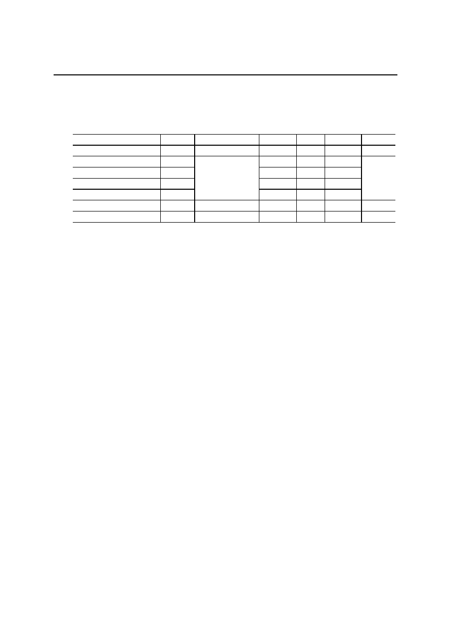
Power Consumption
The values in the following charts are measured values in the operating conditions indicated.
The samples were taken during normal operation in ARM mode with all peripheral clocks activated.
Instructions were being executed from external memory.
I
DD_IO
-f
0
5
10
15
20
25
30
35
40
45
50
0
5
10
15
20
25
30
35
f(MHz)
I
DD_
IO
(mA)
V
DD_IO
=3.3V
Ta=25∞C
CL=50pF
V
DD_IO
=3V
V
DD_IO
=3.6V
I
DD_CORE
-Ta
0
5
10
15
20
25
30
-50
-25
0
25
50
75
100
Ta(∞C)
I
DD
_
CORE
(mA)
f=16MHz
V
DD_CORE
=2.5V
V
DD_CORE
=2.75V
V
DD_CORE
=2.25V
I
DD_IO
-Ta
0
5
10
15
20
25
30
-50
-25
0
25
50
75
100
Ta(∞C)
I
DD
_
IO
(mA)
f=16MHz
CL=50pF
V
DD_IO
=3.6V
V
DD_IO
=3.3V
V
DD_IO
=3V
I
DD_CORE
-f
0
5
10
15
20
25
30
35
40
45
50
0
5
10
15
20
25
30
35
f(MHz)
I
DD_
CORE
(mA)
V
DD_CORE
=2.5V
Ta=25∞C
V
DD_CORE
=2.75V
V
DD_CORE
=2.25V
FEDL674000-02
OKI Semiconductor
ML674000
20/24
Analog-to-Digital Converter Characteristics
(V
DD_CORE
= 2.50 V, V
DD_IO
= 3.3 V, Ta = 25
∞C)
Item
Symbol
Conditions
Minimum Typical Maximum
Unit
Resolution n
--
--
--
10
bit
Linearity error
E
L
--
±3
--
Differential linearity error
E
D
--
±3
--
Zero scale error
E
ZS
--
±3
--
Full scale error
E
FS
Analog input source
impedance
Ri 1k
-- ±3 --
LSB
Conversion time
t
CONV
-- 5
--
--
µs
Throughput
--
10
--
200
kHz
Note: VDD_IO and AVDD should be supplied separately.
∑ Definition of Terms
(1) Resolution: Minimum input analog value recognized. For 10-bit resolution, this is (V
REF
≠
Aground)
˜ 1024.
(2) Linearity error: Difference between the theoretical and actual conversion characteristics.
(Note that it does not include quantization error.) The theoretical conversion characteristic
divides the voltage range between V
REF
and AGND into 1024 equal steps.
(3) Differential linearity error: Difference between the theoretical and actual input voltage change
producing a 1-bit change in the digital output anywhere within the conversion range. This is an
indicator of conversion characteristic smoothness. The theoretical value is (V
REF
≠ Aground)
˜ 1024.
(4) Zero scale error: Difference between the theoretical and actual conversion characteristics at
the point where the digital output switches from "0x000" to "0x001."
(5) Full scale error: Difference between the theoretical and actual conversion characteristics at the
point where the digital output switches from "0x3FE" to "0x3FF."
FEDL674000-02
OKI Semiconductor
ML674000
21/24
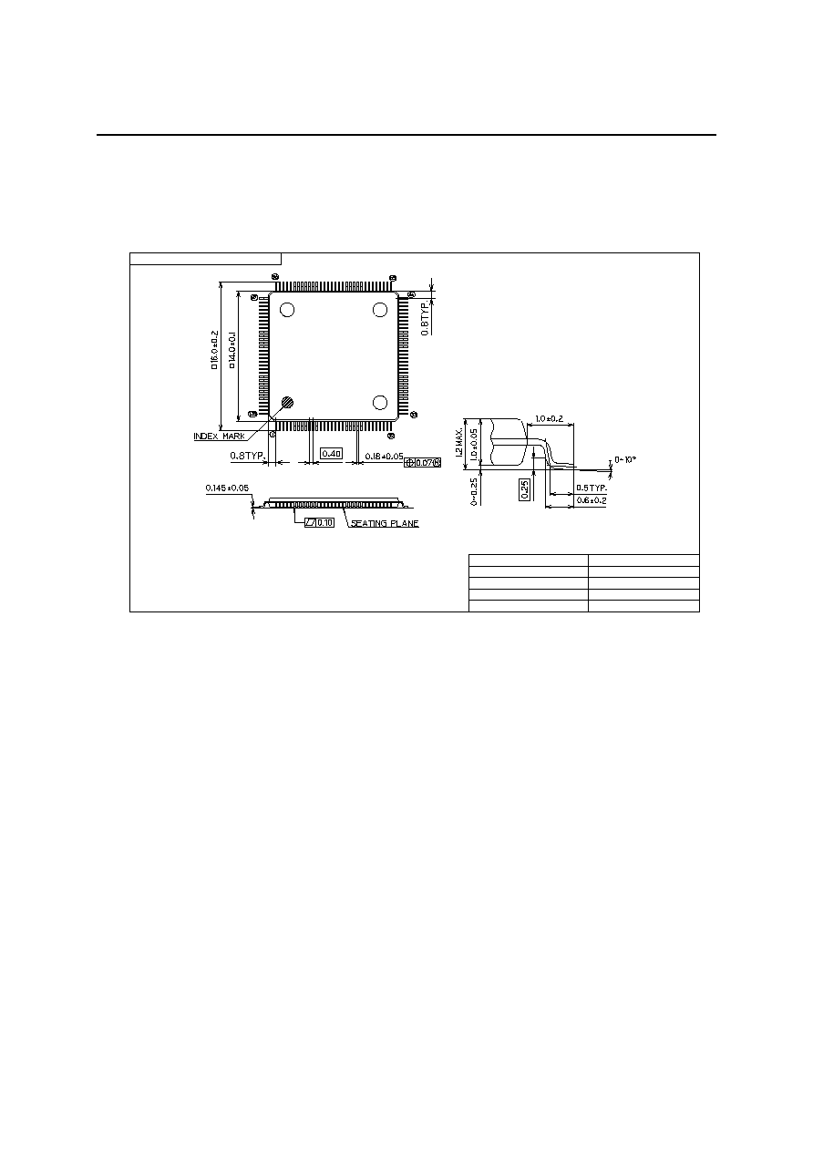
PACKAGE DIMENSIONS
TQFP128-P-1414-0.40-K
Mirror finish
Package material
Epoxy resin
Lead frame material
42 alloy
Pin treatment
Solder plating (
5µm)
Package weight (g)
0.55 TYP.
5
Rev. No./Last Revised
1/Nov. 18, 1999
(Unit : mm)
FEDL674000-02
OKI Semiconductor
ML674000
22/24
Notes for Mounting the Surface Mount Type Package
The surface mount type packages are very susceptible to heat in reflow mounting and humidity
absorbed in storage.
Therefore, before you perform reflow mounting, contact Oki's responsible sales person for the product
name, package name, pin number, package code and desired mounting conditions (reflow method,
temperature and times).

FEDL674000-02
OKI Semiconductor
ML674000
23/24
REVISION HISTORY
Page
Document
No.
Date
Previous
Edition
Current
Edition
Description
PEDL674000-01
Oct., 2001
≠
≠
Preliminary edition 1
≠
≠
Preliminary edition 2
1
1
Feature Table rewritten.
2-13
2-12
Pin names are changed.
14-16 13-15
Description
rewritten.
PEDL674000-02
May 17, 2002
17
16-37
Electrical characteristics added.
≠
≠
Final edition 1
1
1
Number of interrupt sources corrected.
8
8
TBE signal description corrected.
8 8
Pin numbers of XA[23:19] and XA[18:0]
corrected.
FEDL674000-01
Aug. 8, 2002
15-36 15-50
Description
rewritten.
≠
≠
Final edition 2
1
1 to 2
Description changed.
Supported DRAM area changed from 16Mbytes
to 64Mbytes.
Add 144-pin LFBGA package.
≠
5
Add Pin layout for LFBGA package.
4 to 7
6 to 9
Change table of pin list.
(Add LFBGA description and correct some
misdescription.)
8 to 11
10 to 13
Change table of pin description.
(Correct some misdescription.)
12 to 14
14 to 16
Description changed.
18 to 50
≠
Description of AC characteristics Deleted.
Please refer to User's Manual.
51 21
The values of Zero scale error and Full scale
error of Analog-to-Digital converter are
corrected.
FEDL674000-02
Dec. 10, 2002
≠
23
Add Package Dimensions for LFBGA package.

FEDL674000-02
OKI Semiconductor
ML674000
24/24
NOTICE
1. The information contained herein can change without notice owing to product and/or technical improvements.
Before using the product, please make sure that the information being referred to is up-to-date.
2. The outline of action and examples for application circuits described herein have been chosen as an
explanation for the standard action and performance of the product. When planning to use the product, please
ensure that the external conditions are reflected in the actual circuit, assembly, and program designs.
3. When designing your product, please use our product below the specified maximum ratings and within the
specified operating ranges including, but not limited to, operating voltage, power dissipation, and operating
temperature.
4. Oki assumes no responsibility or liability whatsoever for any failure or unusual or unexpected operation
resulting from misuse, neglect, improper installation, repair, alteration or accident, improper handling, or
unusual physical or electrical stress including, but not limited to, exposure to parameters beyond the specified
maximum ratings or operation outside the specified operating range.
5. Neither indemnity against nor license of a third party's industrial and intellectual property right, etc. is
granted by us in connection with the use of the product and/or the information and drawings contained herein.
No responsibility is assumed by us for any infringement of a third party's right which may result from the use
thereof.
6. The products listed in this document are intended for use in general electronics equipment for commercial
applications (e.g., office automation, communication equipment, measurement equipment, consumer
electronics, etc.). These products are not, unless specifically authorized by Oki, authorized for use in any
system or application that requires special or enhanced quality and reliability characteristics nor in any
system or application where the failure of such system or application may result in the loss or damage of
property, or death or injury to humans.
Such applications include, but are not limited to, traffic and automotive equipment, safety devices, aerospace
equipment, nuclear power control, medical equipment, and life-support systems.
7. Certain products in this document may need government approval before they can be exported to particular
countries. The purchaser assumes the responsibility of determining the legality of export of these products
and will take appropriate and necessary steps at their own expense for these.
8.
No part of the contents contained herein may be reprinted or reproduced without our prior permission.
Copyright 2002 Oki Electric Industry Co., Ltd.