
OKI Semiconductor
FEDR57T00101F-02-03
Issue Date: September 17, 2004
MR57T00101F
P2ROM MultiMediaCard
1/24
1. GENERAL
DESCRIPTION
P2ROM MMC stands for P2ROM MultiMediaCard in which an Oki Original Product P2ROM is embedded.
P2ROM (Production Programmed ROM) utilizes Oki unique memory cell, which is an exclusive Oki technology.
Unlike MASKROM, no mask charges apply; Unlike OTP and Flash memory, no additional programming cost is
required.
Features
�
Compliant with MMCA standard (Version 3.1)
�
Card name/capacity
1MB P2ROM MMC: MR57T00101F-xxxKB
�
Operating voltage: 2.7V~3.6V
�
Outside dimension: 32(D)
�24(W)�1.4(H)mm
Notice
This product is different from Secure MMC.
Applications
P2ROM MMC is applied to devices embedded with MultiMediaCard Slot, e.g. Mobile phone,
Electronic dictionary, Game machine, etc.

FEDR57T00101F-02-03
OKI Semiconductor
MR57T00101F / P2ROM MMC
2/24
2. BLOCK
DIAGRAM
GND
VDD
Interface Driver
1
2
3
4
5
6
7
Memory Controller
Register
OCR [31:0]
CID[127:0]
RCA [15:0]
CSD[127:0]
Card
Interface
Controller
Power on R
e
s
e
t
P2ROM
GND

FEDR57T00101F-02-03
OKI Semiconductor
MR57T00101F / P2ROM MMC
3/24
3. PIN
DESCRIPTIONS
MMC Mode
SPI Mode
Pin No
Symbol
Type
Function
Symbol
Type
Function
1 RSV NC
Reserved
CS Input
Chip
select
(50K Pull-up)
2 CMD Input/
Output
Command/Response
(Output: 8mA)
DI Input
Data
in
3
VSS
S
Supply voltage ground
VSS
S
Supply voltage ground
4
VDD
S
Supply voltage
VDD
S
Supply voltage
5 CLK Input
Clock
SCLK Input
Clock
6
VSS
S
Supply voltage ground
VSS
S
Supply voltage ground
7 DAT Input/
Output
Data
(Output: 8mA)
DO Output
Data
out
(Output: 8mA)
Note: No. 6 pin is used to supply Vpp when writing data into P2ROM. It should be connected to GND for general
use.

FEDR57T00101F-02-03
OKI Semiconductor
MR57T00101F / P2ROM MMC
4/24
4. COMMAND
4.1 Command Format (MMC Mode/SPI Mode)
Bit position
47
46
[45:40] [39:08]
[07:01] 00
Bit width
1
1
6
32
7
1
Value "0" "1"
x
x x "1"
Description
Start bit
Transmission bit
Command index
Argument
CRC7
End bit
4.2 Command Class (MMC Mode)
0 1 2 3 4
7
9
10
11
12
13
15
16 17 18 20
23
Class 0 Basic
+
+
+
+
+
+
+
+
+
+
+
Class 1
Stream
read
+
Class 2
Block
read
+
+
+
+
4.3 Command Class (SPI Mode)
0 1 9 10
12
13
16
17 18 23 58
59
Class
0 Basic
+ + + + + + +
Class
1 Non
support
Class
2 Block
read
+ + + + +

FEDR57T00101F-02-03
OKI Semiconductor
MR57T00101F / P2ROM MMC
5/24
4.4 Command
-1/3
MMC mode
SPI mode
CMD Abbreviation
Command
Description
Type
Argument
Resp Argument Resp
0 GO_IDLE_STATE
Resets all cards to Idle
state.
When CS signal is set in
Low state, the card transits
to SPI mode after receiving
this command.
bc [31:00]
stuff bits
- None R1
1
SEND_OP_COND
Asks the card to send an R3
response including OCR
data. The operation voltage
span of the card can be got
according to OCR data.
Moreover, the highest-order
1 bit of OCR is used to
check whether the internal
processing of the card is
finished or not (Ready /Busy
polling).
bcr [31:00]
OCR
without
busy
R3 None
R1
2
ALL_SEND_CID
Asks the cards in Ready
state to send their CID
numbers.
The numbers are sent to
CMD signal when the card
is in MMC mode. When
every 1 bit is transferred,
the CMD signal state is
compared with the state
within the card. If different,
data transmission stops,
and the card returns to
Ready state. If matched, the
card recognizes itself
selected and transits to
Identification state.
bcr [31:00]
stuff bits
R2 - -
3
SET_RELATIVE_ADDR Assigns Relative Card
Address (RCA) to the card
in Identification state.
When RCA is assigned, the
card transits to Stand-by
state, and does not
respond to following CMD2
& CMD3.
ac [31:16]
RCA
[15:00]
stuff bits
R1 - -

FEDR57T00101F-02-03
OKI Semiconductor
MR57T00101F / P2ROM MMC
6/24
4.5 Command-2/3
MMC mode
SPI mode
CMD Abbreviation
Command
Description
Type
Argument
Resp Argument
Resp
4
NOP (SET_DSR)
This command is for setting
DSR (Drive State Register).
But this card does not
support DSR.
bc [31:16]
DSR
[15:00]
stuff bits
- - -
7 SELECT/
DESELECT_CARD
Selects a card and toggles
it between the Stand-by and
Transfer states.
When given an assigned
RCA, the card transits from
Stand-by state to Transfer
state, and responds to the
following read and other
commands. When given an
unassigned RCA, the card
transits to Stand-by state.
When RCA=0000h, the
card transits to Stand-by
state unconditionally.
ac [31:16]
RCA
[15:00]
stuff bits
R1 - -
9
SEND_CSD
Asks the card to send its
CSD data.
ac [31:16]
RCA
[15:00]
stuff bits
R2 None R1
10
SEND_CID
Asks the card to send its
CID data.
ac [31:16]
RCA
[15:00]
stuff bits
R2 None R1
11 READ_DAT_UNTIL_STOP Asks the card to transfer
P2ROM data from the given
address, until interrupted by
CMD12.
adtc
[31:00]
data
address
R1 - -

FEDR57T00101F-02-03
OKI Semiconductor
MR57T00101F / P2ROM MMC
7/24
4.4 Command-3/3
MMC mode
SPI mode
CMD Abbreviation
Command
Description
Type
Argument
Resp Argument Resp
12 STOP
_TRANSMISSION
Forces the card to stop
processing of CMD11 and
CMD18.
ac [31:00]
stuff bits
R1 None
R1
13
SEND_STATUS
Asks the card to send the
information of its status
register.
ac [31:16]
RCA
[15:00]
stuff bits
R1 None
R2
15 GO_INACTIVE
_STATE
Sets the card to inactive
state.
ac [31:16]
RCA
[15:00]
stuff bits
- - -
16
SET_BLOCKLEN
Sets the block length for
following CMD17& CMD18.
ac [31:00]
block
length
R1 [31:00]
block
length
R1
17 READ_SINGLE
_BLOCK
Asks the card to transfer a
data block from the address
assigned by argument. (The
block length is set by
CMD16).
adtc
[31:00]
data
address
R1 [31:00]
data
address
R1
18 READ_MULTIPLE
_BLOCK
Asks the card to transfer data
blocks continuously from the
address assigned by
argument until interrupted by
CMD12. (The block length is
set by CMD16)
adtc
[31:00]
data
address
R1 [31:00]
data
address
R1
23
SET_BLOCK_COUNT
Sets number of blocks to be
transferred for immediately
following CMD18.
ac [31:16]
set to 0
[15:00]
number of
block
R1 [31:16]
set to 0
[15:00]
number of
block
R1
58
READ_OCR
Asks the card to transfer OCR
data.
- - -
None R3
59
CRC_ON_OFF
Makes CRC option to be ON
/OFF. The default in SPI
mode is CRC OFF.
[CRC option bit = 1] means
CRC ON;
[CRC option bit = 0] means
CRC OFF.
- - -
[31:01]
stuff bits
[00:00]
CRC
option
R1

FEDR57T00101F-02-03
OKI Semiconductor
MR57T00101F / P2ROM MMC
8/24
5. RESPONSES (MMC MODE)
5.1 R1
response
Object
commands
CMD3: SET_RELATIVE_ADDR
CMD11: READ_DAT_UNTIL_STOP
CMD12: STOP_TRANSMISSION
CMD13: SEND_STATUS
CMD16: SET_BLOCKLEN
CMD17: READ_SINGLE_BLOCK
CMD18: READ_MULTIPLE_BLOCK
CMD23: SET_BLOCK_COUNT
Bit position
47
46
[45:40] [39:08]
[07:01] 0
Bit width
1
1
6
32
7
1
Value "0" "0"
x
x x "1"
Description
Start bit
Transmission bit
Command index
Card status
CRC7
End bit
5.2 R2
response
Object
commands
CMD2: ALL_SEND_CID
CMD9: SEND_CSD
CMD10: SEND_CID
Bit position
135
134
[133:128] [127:1] 0
Bit width
1
1
6
127
1
Value "0" "0" "111111"
x
"1"
Description
Start bit
Transmission bit
Reserved
CID or CSD register
Internal CRC
End bit
5.3 R3
response
Object
commands
CMD1:
SEND_OP_COND
Bit position
47
46
[45:40] [39:08] [07:01] 0
Bit width
1
1
6
32
7
1
Value "0" "0" "111111" x
"1111111"
"1"
Description
Start bit
Transmission bit
Reserved
OCR register
Reserve
End bit

FEDR57T00101F-02-03
OKI Semiconductor
MR57T00101F / P2ROM MMC
9/24
5.4 Card Status (MMC Mode)
Bit Identifier
type Value
Description
CC
31
out_of_range
ER
"0"= no error
"1"= error
The command's argument was out of the
allowed range for this card.
C
30
address_error
ERX "0"= no error
"1"= error
A misaligned address which did not match the
block length was used in the command.
C
29
block_len_error
ER
"0"= no error
"1"= error
The transferred block length is not allowed for
this card, or the number of transferred bytes
does not match the block length.
C
[28:24] - - x Don't
care.
-
23
com_CRC_error
ER
"0"= no error
"1"= error
The CRC check in the immediately previous
command failed.
B
22
illegal_command
ER
"0"= no error
"1"= error
Command is not legal for the card state.
B
[21:13] - - x Don't
care.
-
[12:09] current_state
SX "0000"=
idle
"0001"= ready
"0010"= ident
"0011"- stby
"0100"= tran
"0101"= data
Others: reserve
Current state of the card.
B
[08:00] - - x Don't
care.
-
5.5 Card status field / command � cross reference (MMC Mode)
Response Format 1 Status bit #
CMD
31 30 29 23 22 12:9
3 x x x
7 x x x
11 x x x x x
12 x x x
13 x x x x x
16 x x x x
17 x x x x x
18 x x x x x
23 x x x
FEDR57T00101F-02-03
OKI Semiconductor
MR57T00101F / P2ROM MMC
10/24
5.6 Card State Transition Table (MMC Mode)
current state
idle
ready
ident
stby
tran data ina
command changes
to
class independent
CRC error
-
-
-
-
-
-
-
command not supported
-
-
-
-
-
-
-
class 0
CMD0 idle
idle
idle
idle
idle
idle
-
CMD1, card VDD range compatible
ready
-
-
-
-
-
-
CMD1, card is busy
idle
-
-
-
-
-
-
CMD1, card VDD range not compatuble
ina
-
-
-
-
-
-
CMD2, card wins bus
-
ident
-
-
-
-
-
CMD2, card loses bus
-
ready
-
-
-
-
-
CMD3 -
-
stby
-
-
-
-
CMD4 -
-
-
stby
-
-
-
CMD7, card is addressed
-
-
-
tran
-
-
-
CMD7, card is not addressed
-
-
-
-
stby stby
-
CMD9 -
-
-
stby
-
-
-
CMD10 -
-
-
stby
-
-
-
CMD12 -
-
-
-
-
tran
-
CMD13 -
-
-
stby
tran
data
-
CMD15 -
-
-
ina
ina
ina
-
class 1
CMD11 -
-
-
-
data
-
-
class 2
CMD16 -
-
-
-
tran
-
-
CMD17 -
-
-
-
data
-
-
CMD18 -
-
-
-
data
-
-
CMD23 -
-
-
-
tran
-
-

FEDR57T00101F-02-03
OKI Semiconductor
MR57T00101F / P2ROM MMC
11/24
6. RESPONSES (SPI MODE)
6.1 R1
response
Object
commands
CMD0: GO_IDLE_STATE
CMD1: SEND_OP_COND
CMD9: SEND_CSD
CMD10: SEND_CID
CMD12: STOP_TRANSMISSION
CMD16: SET_BLOCKLEN
CMD17: READ_SINGLE_BLOCK
CMD18: READ_MULTIPLE_BLOCK
CMD23: SET_BLOCK_COUNT
CMD59: CRC_ON_OFF
7 6 5 4 3 2 1 0
0 0 0
in Idle state
illegal command
communication CRC error
address error
parameter error
6.2 R2
response
Object
commands
CMD13: SEND_STATUS
15 14 13 12 11 10 9 8 7 6 5 4 3 2 1 0
0
0
0
0 0 0 0 0 0 0
Out of Range
in Idle state
illegal command
communication CRC error
address error
parameter error
6.3 R3
response
Object
commands
CMD58: READ_OCR
39 38 37 36 35 34 33 32 31 0
0 0 0
OCR
in Idle state
illegal command
communication CRC error
address error
parameter error

FEDR57T00101F-02-03
OKI Semiconductor
MR57T00101F / P2ROM MMC
12/24
6.4 Data Tokens (SPI Mode)
Data tokens are 4 to (N+3) bytes long (Where N is the data block length set by SET_BLOCK_LENGTH
Command) and have the following format:
Bit Position
Token Type
Transaction Type
7 6 5 4 3 2
1
0
Start Block
Single Block Read
1
1
1
1
1
1
1
0
Start Block
Multiple Block Read
1
1
1
1
1
1
1
0
6.5 Data Error Token
If a read operation fails or the given data is not accepted, following Data Error Token is sent:
7 6 5 4 3 2 1 0
0 0 0 0 0 0 0
Out of Range
Data
Response
Token Type
(1byte)
Data
(512Bytes)
CRC
(2bytes)

FEDR57T00101F-02-03
OKI Semiconductor
MR57T00101F / P2ROM MMC
13/24
6.6 Card Status (SPI Mode)
Bit Identifier
type Value
Description
CC
15 - - 0
"0"
always
-
14
parameter error
ERX "0"= no error
"1"= error
An error occurred in command's parameters.
C
13
address error
ERX "0"= no error
"1"= error
A misaligned address which did not match the
block length was used in the command.
C
12 - - x
Don't
care.
-
11
com crc error
ER
"0"= no error
"1"= error
The CRC check in the immediately previous
command failed.
C
10
illegal command
ER
"0"= no error
"1"= error
Command is not legal for the card state.
C
-
-
x
Don't
care.
-
08
idle state
SR
"0"= card is ready
"1"= card is in
idle state
A
07
out_of_range
ER
"0"= no error
"1"= error
The command's argument was out of the
allowed range for this card.
C
[06:00] - - x Don't
care.
-

FEDR57T00101F-02-03
OKI Semiconductor
MR57T00101F / P2ROM MMC
14/24
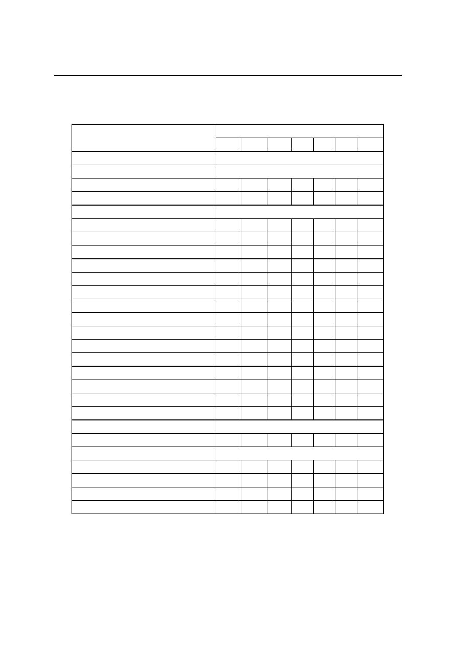
7. REGISTERS
7.1 OCR register (Operation conditions register)
OCR-slice Field Value
Remarks
31
Status after power up
0 or 1
[31:24] reserved
0
23
3.5 � 3.6V
1
22
3.4 � 3.5V
1
21
3.3 � 3.4V
1
20
3.2 � 3.3V
1
19
3.1 � 3.2V
1
18
3.0 � 3.1V
1
17
2.9 � 3.0V
1
16
2.8 � 2.9V
1
15
2.7 � 2.8V
1
14
2.6 � 2.7V
0
13
2.5 � 2.6V
0
12
2.4 � 2.5V
0
11
2.3 � 2.4V
0
10
2.2 � 2.3V
0
09
2.1 � 2.2V
0
08
2.0 � 2.1V
0
07
1.9 � 2.0V
0
06
1.8 � 1.9V
0
05
1.7 � 1.8V
0
04
1.65 � 1.70V
0
03
1.60 � 1.65V
0
02
1.55 � 1.60V
0
01
1.50 � 1.55V
0
00
1.45 � 1.50V
0
7.2 CID register (Card identification register)
This register uses the data written in P2ROM's particular field.
CID-slice Name Field
Bit
Width
Value OKI
original
[127:120] Manufacture ID
MID
8
0x41
OKI ID Assigned by MMCA
[119:104] OEM/Application
ID
OID
16
0x0000
OKI Device Name
[103:56] Product name
PNM
48
P2 001
Product Name
[55:48] Product
revision
PRV
8 0x10
Rev. of Product (version 1.0)
[47:16] Product
serial
number PSN 32 0x00000001
Product serial numer
Default=1, settable
[15:8] Manufacturing
data MDT
8
Month of receiving
Code file
Date OKI recieved Code file
from customer or Programmed
[7:1]
7-bit CRC checksum
CRC7
7
CRC
check sum
[0:0]
-
-
1
1
" 1" always

FEDR57T00101F-02-03
OKI Semiconductor
MR57T00101F / P2ROM MMC
15/24
7.3 CSD register (Card-Specific Data register)
This register uses the data written in P2ROM's particular field.
Value
CSD-slice Name
Filed
Bit
width
Bin. Hex.
Type Remarks
[127:126] CSD
Structure
CSD_STRUCTURE 2 10 0x2
R
Version
3.1
[125:122] spec
version
SEPC_VERS 4
0011
0x3
R
Version
3.1
[121:120] reserved
2
X
X
R Don't
care
[119:112]
data read access
time1
TAAC 8
00001000
0x08
R
1ns
[111:104]
data read access
time2
NSAC 8
00000001
0x01
R
100cycles
[103:96]
max data transfer
rate
TRAN_SPEED 8
00101010
0x2A
R
20Mb/s
[95:84]
card command class
CCC
12
000000000111
0x007
R
Support
Class0,1,2
[83:80]
max read data block
length
READ_BL_LEN 4
1001
0x9
R
512bytes
79
partial blocks for read
allowed
READ_BL_PARTIAL 1 1 0x1
R
78 reserved
1
X
X R
Don't
care
77 read
block
misalignment
READ_BLK_MISALIGN 1
0
0x0
R
Crossing
block is not
allowed
76 DSR
implemented DSR_IMP
1
0
0x0 R
DSR:
Non support
[75:74] reserved
2
X
X
R Don't
care
[73:62] device
size
C_CIZE
12 000111111110
0x1FE R
[61:59]
min. read current
VDD_R_CURR_MIN 3 000 0x0
R
0.5mA
[58:56] max.
read
current VDD_R_CURR_MAX 3 100 0x4
R
35mA
[55:50] reserved
6
X
X
R Don't
care
[49:47]
device size multiplier
C_SIZE_MULT
3
000
0x0
R
[46:31] reserved
16
X
X
R Don't
care
[30:29] manufacture
default
ECC
DEFAULT_ECC 2
00
0x0
R
ECC:
Non support
[28:26] reserved
3
X
X
R Don't
care
[25:22] Max.
write
data
block length
WRITE_BL_LEN 4
1001
0x9
R
[21:16] reserved
6
X
X
R Don't
care
15
file format group
FILE_FORMAT_GRP
1
0
0x0
R
14
Copy flag (OTP)
COPY
1
0
0x0
R
Default=0,
settable
13 permanent
write
protection
PERM_WRITE_PROTEC
T
1 1 0x1
R
12 temporary
write
protection
TMP_WRITE_PROTECT 1
1
0x1 R
[11:10] file
format
FILE_FORMAT
2
00
0x0 R Default=0,
settable
[9:8] ECC
code
ECC
2
00
0x0 R ECC:
Non support
[7:1] CRC
CRC
7
CRC
CRC R
0 reserved
1
1
0x1 R

FEDR57T00101F-02-03
OKI Semiconductor
MR57T00101F / P2ROM MMC
16/24
*1 Card Capacity
Name Card
Capacity
C_SIZE_MULT
C_SIZE
MULT
BLOCKNR
BLOCK_LEN
MR57T00101F 1MB
0
510 4
2044
512
Cross reference of CSD fields vs command class
Command Classes
CSD Field
0 1 2
CSD_STRUCTURE +
+
+
SEPC_VERS +
+
+
TAAC
+
+
NSAC
+
+
TRAN_SPEED
+
+
CCC +
+
+
READ_BL_LEN
+
READ_BL_PARTIAL
+
READ_BLK_MISALIGN
+
DSR_IMP +
+
+
C_CIZE
+
+
VDD_R_CURR_MIN
+
+
VDD_R_CURR_MAX
+
+
DEFAULT_ECC
+
+
FILE_FORMAT_GRP....
COPY +
+
+
PERM_WRITE_PROTECT +
+
+
TMP_WRITE_PROTECT +
+
+
FILE_FORMAT
ECC
+
+
CRC +
+
+

FEDR57T00101F-02-03
OKI Semiconductor
MR57T00101F / P2ROM MMC
17/24
8. ELECTRICAL
CHARACTERISTICS
8.1 General
Parameter Symbol
Min
Max
Unit
Remarks
Peak voltage on all line
-0.3
4.6
V
Absolute maximum
rating
Input Leakage Current
-10
10
�A
Input Leakage Current for CS signal
200
�A
Output Leakage Current
-10
10
�A
8.2 Recommended operating conditions
Parameter Symbol
Min
Max
Unit
Remarks
Power supply voltage
VDD
2.7
3.6
V
Operating frequency (Identification Mode)
FOD
400
KHz
Operating frequency (Data Transfer Mode)
Fpp
20
MHz
Operating temperature
Ta
-10
85
�
C
Storage temperature
Tstg
-40
85
�
C Absolute
maximum
rating
8.3 Open-Drain Bus Signal Level
Parameter Symbol
Min
Max Unit Condition
Output LOW voltage
VOL
0.3
V
IOL=2mA
8.4 Push-Pull bus signal level
Parameter Symbol
Min
Max Unit Condition
Output HIGH voltage
VOH
VDD-0.2
V
IOH=-100�A
@VDD min
Output LOW voltage
VOL
0.125*VDD
V
IOL=100�A
@VDD min
Input HIGH voltage
VIH
0.625*VDD
VDD+0.3
V
Input LOW voltage
VIL
VSS-0.3 0.25*VDD V

FEDR57T00101F-02-03
OKI Semiconductor
MR57T00101F / P2ROM MMC
18/24
8.5 Bus Signal Line Load
Parameter Symbol
Min
TYP Max
Unit
Condition
Pull-up resistance for CS
Rcs
50
K
Bus signal line capacitance
CL
250
pF
Fpp<= 5MHz
Bus signal line capacitance
CL
100
pF
Fpp<= 20MHz
Signal card capacitance
C_CARD
19
pF
8.6 Supply
Current
Parameter Symbol
Min
Max Unit
Condition
Supply Current
IDD
30
mA
VDD=2.7~3.6V,
Ta=-10~85
�
C
at 20MHz
Supply Current
IDDS
200
�A VDD=2.7~3.6V,
CS=VDD,
VIH=VDD, VIL=Vss,
Ta=-10~85
�
C
at 0MHz (standby)
FEDR57T00101F-02-03
OKI Semiconductor
MR57T00101F / P2ROM MMC
19/24
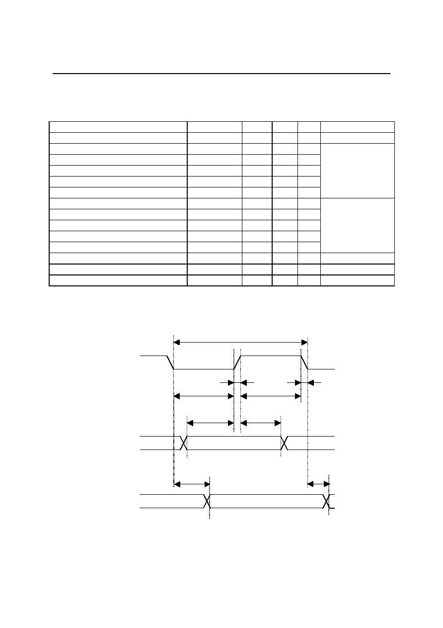
8.7 AC
Characteristics
(VDD=2.7~3.6V,Ta =-10~+85
�
C)
Parameter Symbol
Min
Max
Unit
Remarks
Clock frequency (Identification Mode)
FOD
0
400
KHz
Clock frequency (Data Transfer Mode)
Fpp
20
MHz
Clock Low time
tWL
10
ns
Clock High time
tWH
10
ns
Clock rise time
tTLH
10
ns
Clock fall time
tTHL
10
ns
CL<=100pF
Clock frequency (Data Transfer Mode)
Fpp
5
MHz
Clock Low time
tWL
50
ns
Clock High time
tWH
50
ns
Clock rise time
tTLH
50
ns
Clock fall time
tTHL
50
ns
CL<=250pF
Input set-up time
tISU
3
ns
Input hold time
tIH
3
ns
Output set-up time
tdly
0
15
ns
INPUT
OUTPUT
tWH
tISU
tPP
tWL
tIH
tdly
tdly
CLOCK
tTLH
tTHL
FEDR57T00101F-02-03
OKI Semiconductor
MR57T00101F / P2ROM MMC
20/24
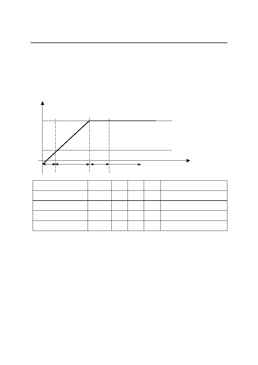
9. POWER
UP
Power up sequence is shown below.
Circuit for detecting power-supply voltage is embedded in this MMC. When the voltage is below a certain value,
power-on reset is generated in order to prevent operation error. As long as enough voltage is reached, the internal
initialization is done automatically.
Parameter Symbol
Min
Max
Unit
Remarks
Min VCC for logic
Vmin
1.5
V
Power up time-1
t1
Clock-supply is not allowed
Power up time-2
t1+t2
1
ms
Initialize time
t2+t3
37
clock
10. SHORTCUT PROTECTION
Cards shall be inserted/removed into/from the bus without damage. If one of the supply pins (VDD or VSS) is not
connected properly, then the current is drawn through a command line or a data line. In such case, the card cannot
work normally.
The device connector for P2ROM MMC insertion should be connected as following steps, for the length of contact
pins is different (length of VSS, VDD > length of other signals).
Step-1: VSS (pin 3), VDD (pin 4) connection
Step-2: Other signals (pin 1~2, 5~7) connection
Minimum operation voltage
for card logic (Vmin)
Vcc
Time
System supply voltage
stable
t1
t2
t3
FEDR57T00101F-02-03
OKI Semiconductor
MR57T00101F / P2ROM MMC
21/24
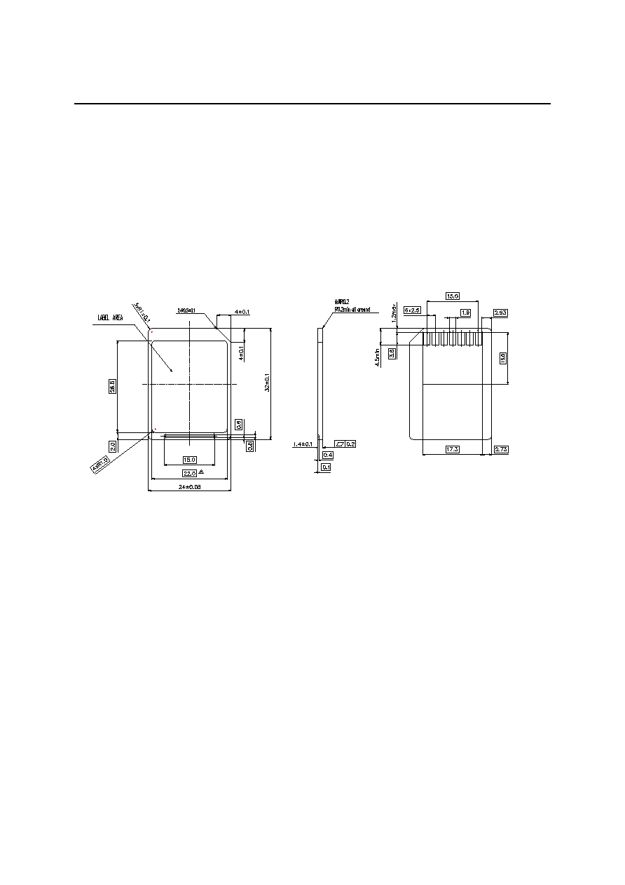
11. CARD DIMENSION DIAGRAM

FEDR57T00101F-02-03
OKI Semiconductor
MR57T00101F / P2ROM MMC
22/24
12. STATE TRANSITION DIAGRAM
CMD0
CMD1
CMD2
Identification
State(ident)
CMD3
Transfer
State(tran)
Idle State
(idle)
CMD11
CMD18
CMD17
CMD16
CMD23
GO_IDLE_STATE
SEND_OP_COND
ALL_SEND_CID
SET_RELATIVE_ADDR
NOP
SEND_CSD
SEND_CID
SELECT/DESELECT_CARD
READ_DAT
_UNTIL_STOP
READ_SINGLE_BLOCK
READ_MULTIPL
E_BLOCK
Sending-data
State(data)
CMD7
CMD12
CMD7
SELECT/DESELE
CT_CARD
STOP
_TRANSMISSION
SET_BLOCKLEN
SET_BLOCK
_COUNT
CMD15
GO_INACTIVE_STATE
Inactive
State(ina)
Power ON
Non compatible voltage range
card loose bus
Ready State
(ready)
MMC mode
SPI mode
CS signal="0"
CMD1
SEND_OP_COND
CMD9
CMD10
SEND_CSD
CMD4
CMD9
CMD10
CMD7
CMD13
SEND_STATUS
CMD13
SEND_STATUS
SELECT/DESELECT
_CARD
SELECT/DESELECT
_CARD
CMD58
READ_OCR
CMD7
CMD18
CMD16
CMD23
READ_MULTIPLE
_BLOCK
STOP_TRANSMISSION
SET
_BLOCKLEN
SET_BLOCK
_COUNT
CMD13
SEND_STATUS
CMD17
READ_SINGL
E_BLOCK
CMD59
CMD12
Stand-by
State(stby)
Sending-data
State(data)
SEND_CID
CRC_ON_OFF

FEDR57T00101F-02-03
OKI Semiconductor
MR57T00101F / P2ROM MMC
23/24
REVISION HISTORY
Page
Document No.
Date
Previous
Edition
Current
Edition
Description
FEDR57T00101F-02-01 June 8, 2004
�
�
Final edition 01
1 1
Change
headline
18 18
8.5 Bus Signal Line Load change following:
Bus signal line capacitance:
Condition: delete "30 cards"
Bus signal line capacitance:
Condition: delete "10 cards"
Signal card capacitance: Max 17->19.
FEDR57T00101F-02-02 June 25, 2004
19 19
8.7 AC Characteristics change following:
Remarks: delete (10cards)
Remarks: delete (30cards)
FEDR57T00101F-02-03 Sept.
17, 2004 1 1
Card name/capacity change following:
MR57T00101F -> MR57T00101F-xxxKB

FEDR57T00101F-02-03
OKI Semiconductor
MR57T00101F / P2ROM MMC
24/24
NOTICE
1. The information contained herein can change without notice owing to product and/or technical improvements.
Before using the product, please make sure that the information being referred to is up-to-date.
2. The outline of action and examples for application circuits described herein have been chosen as an explanation
for the standard action and performance of the product. When planning to use the product, please ensure that the
external conditions are reflected in the actual circuit, assembly, and program designs.
3. When designing your product, please use our product below the specified maximum ratings and within the
specified operating ranges including, but not limited to, operating voltage, power dissipation, and operating
temperature.
4. Oki assumes no responsibility or liability whatsoever for any failure or unusual or unexpected operation
resulting from misuse, neglect, improper installation, repair, alteration or accident, improper handling, or
unusual physical or electrical stress including, but not limited to, exposure to parameters beyond the specified
maximum ratings or operation outside the specified operating range.
5. Neither indemnity against nor license of a third party's industrial and intellectual property right, etc. is granted
by us in connection with the use of the product and/or the information and drawings contained herein. No
responsibility is assumed by us for any infringement of a third party's right which may result from the use
thereof.
6. The products listed in this document are intended for use in general electronics equipment for commercial
applications (e.g., office automation, communication equipment, measurement equipment, consumer
electronics, etc.). These products are not, unless specifically authorized by Oki, authorized for use in any
system or application that requires special or enhanced quality and reliability characteristics nor in any system
or application where the failure of such system or application may result in the loss or damage of property, or
death or injury to humans.
Such applications include, but are not limited to, traffic and automotive equipment, safety devices, aerospace
equipment, nuclear power control, medical equipment, and life-support systems.
7. Certain products in this document may need government approval before they can be exported to particular
countries. The purchaser assumes the responsibility of determining the legality of export of these products and
will take appropriate and necessary steps at their own expense for these.
8. No part of the contents contained herein may be reprinted or reproduced without our prior permission.
Copyright 2004 Oki Electric Industry Co., Ltd.