 | –≠–ª–µ–∫—Ç—Ä–æ–Ω–Ω—ã–π –∫–æ–º–ø–æ–Ω–µ–Ω—Ç: MSA180RS | –°–∫–∞—á–∞—Ç—å:  PDF PDF  ZIP ZIP |

1/16
MSA180
° Semiconductor
GENERAL DESCRIPTION
The MSA180 is a piezo speaker driver for OKI's speech synthesizers. Its voltage gain can be adjusted
by a factor of up to 10. The differential output provides an amplitude of twice the voltage supply.
A separate output connects to the base of an external transistor for controlling system voltage.
A standby function eliminates power loss when no input signal is present.
FEATURES
∑ Power supply voltage
: 2.0 V to 6.0 V (single supply voltage)
∑ Low current consumption
: 4.2 mA typ (V
CC
=3 V, no load)
∑ Standby current
: <1 mA
∑ Differential output
: Twice the supply voltage (maximum output
amplitube)
∑ Package options :
8-pin plastic DIP (DIP8-P-300-2.54) (Product name: MSA180RS)
8-pin plastic SOP (SOP8-P-250-1.27-K) (Product name: MSA180MS-K)
Chip
BLOCK DIAGRAM
V
CC
MODE1
MODE2
A
IN
GND
Logic
V
CC
V
CC
BASE
SP
SP
2.2 kW
+
≠
A
V
=20
A
V
=20
1.3 kW
6.6 kW
6.6 kW
18 kW
+
≠
° Semiconductor
MSA180
Piezo Speaker Amplifier
E2D0049-39-21
This version: Feb. 1999
Previous version: May. 1997
2/16
MSA180
° Semiconductor
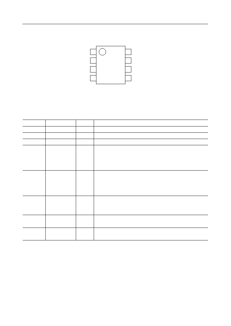
PIN CONFIGURATION (TOP VIEW)
8-Pin Plastic DIP or 8-Pin Plastic SOP
PIN DESCRIPTIONS
1
2
3
4
8
7
6
5
MODE2
A
IN
GND
SP
MODE1
BASE
V
CC
SP
Pin
Type
Description
6
V
CC
--
Power supply pin.
3
GND
--
Ground pin.
2
A
IN
I
Voice signal input pin.
8
MODE1
I
This pin switches the device between operation and standby modes.
The IC is in operation mode if V
IH
> 1.0 V on the MODE1 pin and is in
standby mode if V
IL
< 0.3 V on the MODE1 pin. When MODE1 is used,
MODE2 must be connected to V
CC
.
1
MODE2
I
This pin switches the device between operation and standby modes.
The IC is in operation mode if V
IL
< V
CC
≠1.0 V on MODE1 pin and is in
standby mode if V
IH
> V
CC
≠0.3 V on MODE1 pin. When MODE2 is used
MODE1 must be connected to GND.
7
BASE
O
This pin is connected to the base of an external transistor. If an
external transistor is not used to control system voltage, this pin must
be left open.
4
SP
O
This is a speaker output pin that provides signals with the same phase
as the input.
5
SP
O
This is a speaker output pin that provides signals with an inverted
phase to the input.
Symbol
3/16
MSA180
° Semiconductor
ABSOLUTE MAXIMUM RATINGS
RECOMMENDED OPERATING CONDITIONS
Parameter
Symbol
Condition
Rating
Unit
Remarks
Power Supply Voltage
V
CC
--
≠0.3 to +6.5
V
--
Input Voltage
V
IN
--
≠0.3 to V
CC
+0.3
V
A
IN
MODE1
MODE2
BASE
Maximum Output Current
I
OMAX
V
CC
=3 V
±80
mA
SP, SP
Power Dissipation
P
D
Ta=25∞C
400
mW
DIP type
340
mW
SOP type
Junction Temperature
T
jMAX
--
110
∞C
Chip
Storage Temperature
T
STG
--
≠55 to +150
∞C
--
(Ta=25∞C unless otherwise specified)
Parameter
Symbol
Min.
Max.
Unit
Condition
Power Supply Voltage
V
CC
2.0
6.0
V
--
"L" Input Voltage
V
IL1
--
0.3
V
Applied to MODE1 pin
Operating Temperature
T
op
≠40
+85
∞C
--
Load Impedance
Z
L
200
--
W
--
Peak Load Current
I
O-P
--
±30
mA
--
"H" Input Voltage
V
IH1
1.0
--
V
V
IH2
V
CC
≠0.3
--
V
V
IL2
--
V
CC
≠1.0
V
Applied to MODE2 pin
Applied to MODE1 pin
Applied to MODE2 pin

4/16
MSA180
° Semiconductor
ELECTRICAL CHARACTERISTICS
Parameter
Symbol
Condition
Min.
Typ.
Max.
Unit
Voltage Gain
A
V1
A
IN
∆SP
4.25
5
5.75
V/V
(Ta=25∞C, V
CC
=2 V to 6 V unless otherwise specified)
A
V2
A
IN
∆
SP
4.25
5
5.75
V/V
A
V3
A
IN
∆(SP-SP)
8.5
10
11.5
V/V
A
IN
Input Resistance
R
IN
--
17.2
24.6
32.0
kW
Output DC Voltage
V
CC
=2 V
0.7
1.0
1.3
V
*1
V
CC
=6 V
2.5
3.5
4.6
V
Output DC Offset Voltage
V
CC
=2 V
--
--
0.2
V
*2
V
CC
=6 V
--
--
0.6
V
SP, SP Output "H" Voltage
V
OH
I
OUT
=≠10 mA
V
CC
≠0.25
--
--
V
SP, SP Output "L" Voltage
V
OL
I
OUT
=10 mA
--
--
0.25
V
V
CC
=3 V
Operating Current
I
CC
--
4.2
6.2
mA
Z
L
=∑
BASE=Open
Circuit Current in Standby Mode
I
CCS
A
IN
=Open
--
--
1
µA
MODE1=GND
A
IN
Input DC Bias Voltage
V
AIN
V
CC
=2 V
0.18
0.26
0.34
V
*3
V
CC
=6 V
0.52
0.74
0.96
V
MODE1 "H" Input Current
I
IH1
MODE1=V
CC
--
--
160
µA
MODE2 "H" Input Current
I
IH2
MODE2=V
CC
--
--
1
µA
MODE1 "L" Input Current
I
IL1
MODE1=GND
≠1
--
--
µA
MODE2 "L" Input Current
I
IL2
MODE2=GND
≠160
--
--
µA
Base Output Current
I
BO1
V
CC
=2 V
0.4
--
--
mA
BASE=V
CC
I
BO2
V
CC
=6 V
1.6
--
--
mA
BASE=V
CC
No signal
SP-SP
MODE1=MODE2=GND
or
MODE1=MODE2=V
CC
MODE2=V
CC
V
O
DV
O
*1 Typical value is V
O
= V
CC
• 0.625 ≠ 0.25.
*2 Maximum value is DV
O
= V
CC
• 0.1.
*3 Typical value is V
AIN
= V
CC
• 0.12 + 0.02.

5/16
MSA180
° Semiconductor
APPLICATION CIRCUITS
How to Adjust Gain
Gain control adjustment of the input signal level is shown below. When using OKI's speech
synthesizer devices, insert a diode in series with the variable resistor to reduce pop noise.
The circuit below also implements gain adjustment for a higher impedance signal source.
Signal
R1
100 kW
C1
0.1 mF
A
IN
MSA180
V
DD
BASE
V
CC
SP
SP
GND
MODE1
PIEZO SPEAKER
MODE2
Signal
R1
20 kW
C1
0.1 mF
A
IN
MSA180
V
DD
BASE
V
CC
SP
SP
GND
MODE1
PIEZO SPEAKER
MODE2

6/16
MSA180
° Semiconductor
How to Connect the Piezo Speaker
To achieve the full gain level of 10 V, even at a low supply voltage (V
CC
=3 V), connect a coil in series
with the piezo speaker.
The resonance frequency that occurs in the circuit containing the coil and the piezo speaker is :
f
Q
=
2p C
L
• L
L
1
[Hz]
Where C
L
is the piezo capacitance and L
L
the coil inductance.
For instance, if the piezo capacitance is 0.1 mF and f
Q
is in a range of 2 to 3 kHz, then the coil induct-
ance should be 30 mH.
A
IN
MSA180
V
DD
BASE
V
CC
SP
SP
GND
MODE1
PIEZO SPEAKER
COIL
MODE2
7/16
MSA180
° Semiconductor
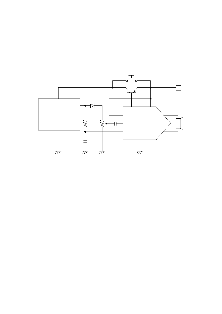
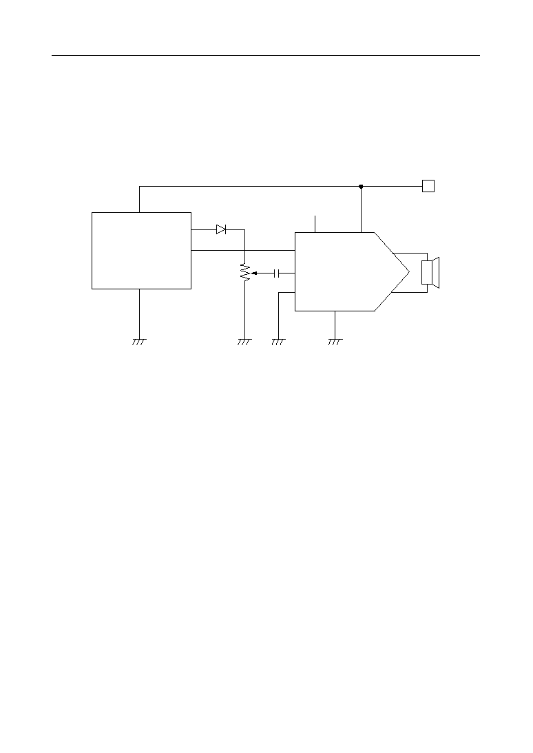
Application Example for Circuits Containing the MSM6378A/MSM6379 Speech Synthesizers
This example shows how to connect the MSA180 with an MSM6378A or MSM6379 speech
synthesizer using an external transistor and the MODE1 pin. The analog output of both synthesizers
lowers to 0 V in their standby mode. For this reason, the voice signal can be used to control operation
and standby modes of the MSA180. The circuit also controls the voltage via an external transistor.
If this function is not used, leave the BASE pin open.
MSM6378A
or MSM6379
V
DD
AOUT
GND
SP
START SWITCH
C1
C2
A
IN
MSA180
V
DD
BASE
V
CC
SP
GND
MODE1
PIEZO SPEAKER
R2
R1
MODE2
Operation Flow
1. When the start switch is pressed, power is supplied to the V
DD
pins on the MSM6378A or
MSM6379, and operation mode is invoked. Voice output level then rises.
2. When operation mode is involved, the voice signal rises above the GND level, and MODE1 on
MSA180 goes high (H).
3. The BASE pin on MSA180 goes low (L) to drive the external transistor for power-supply control.
4. The audio IC continues to operate using the external transistor as a power supply. The device
continues to operate and voice sounds, even if the start switch is released at this time.
5. When the sound ends, MODE1 on MSA180 falls low (L), the voice signal falls to GND level, and
standby mode ensues.
6. The external transistor for power-supply control is switched off, switching the voice synthesizer
off because the power supply is switched off.
8/16
MSA180
° Semiconductor
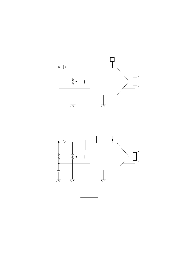
Supplemental Information When Using a Voice Signal on the MODE1 Pin
When using the voice signal on MODE1, as in the circuit below, care must be taken regarding the
voice input level. Application of the voice signal below V
IH1
level to the MODE1 pin causes the
MSA180 to switch into standby mode, interrupting the voice reproduction flow, and causing
undesired noises.
SP
C1
A
IN
MSA180
V
DD
BASE
V
CC
SP
GND
MODE1
PIEZO SPEAKER
R1
MODE2
Signal
When using a voice signal lower than V
IH
, refer to the circuit below. With a low-pass filter consisting
of R2 and C2, voice levels lower than V
IH1
are passed through. However, select values for R2 and C2
such that the input voltage on MODE1 is greater than V
IH2
.
The cutoff frequency of the low-pass filter is calculated as follows:
f
C
=
2p • R2
• C2
1
[Hz]
For instance, if the cutoff frequency is 50 Hz, C2 is 0.1 mF and R2 is 30 kW. For a lower cutoff frequen-
cy, use a larger value for C2 or R2.
SP
C1
C2
A
IN
MSA180
V
DD
BASE
V
CC
SP
GND
MODE1
PIEZO SPEAKER
R2
R1
MODE2
Signal
9/16
MSA180
° Semiconductor
Application Example for Circuits Containing MSM6375/MSM6650 Family Speech Synthesizers
The example below shows how to connect the MSA180 with the MSM6375 or MSM6650 family
speech synthesizers using the synthesizer's BUSY output to control operation and standby mode of
the MSA180. As voice output stops, BUSY rises to the "H" level. For this reason, MODE2 is used to
control operation and standby modes of the MSA180.
Notes: 1. The diode on A
OUT
reduces pop noise.
2. This circuit makes use of the BUSY output of the speech synthesizer.
3. As the voice reproduction stops, BUSY outputs a "H" level to MODE2, setting the stand-
by function.
4. If MODE2 is used, MODE1 must be connected to GND.
5. Leave the BASE pin open if it is not used.
MSM6650
or MSM6375
V
DD
AOUT
GND
SP
C1
A
IN
MSA180
V
DD
BASE
V
CC
SP
GND
MODE1
PIEZO SPEAKER
R1
MODE2
BUSY

10/16
MSA180
° Semiconductor
Application Example for Circuits Containing the MSM6388/MSM6588 Speech Recorders
The example below shows how to connect the MSA180 with the MSM6388 or MSM6588 family
speech recording ICs using the recorders' STBY output to control operation and standby mode of the
MSA180. As voice output stops, STBY rises to the "H" level. For this reason, MODE2 is used to control
operation and standby modes of the MSA180.
Notes: 1. The diode on A
OUT
reduces pop noise.
2. This circuit makes use of the STBY output of the speech synthesizer.
3. As the voice reproduction stops, STBY outputs a "H" level to MODE2, setting the stand-
by function.
4. If MODE2 is used, MODE1 must be connected to GND.
5. Leave the BASE pin open if it is not used.
MSM6388
or MSM6588
V
DD
AOUT
GND
SP
C1
A
IN
MSA180
V
DD
BASE
V
CC
SP
GND
MODE1
PIEZO SPEAKER
R1
MODE2
CS3(STBY)

11/16
MSA180
° Semiconductor
Application Examples for Circuits Containing a Microcontroller or Other Peripheral
Devices
The circuit below uses a voice signal which rises high in operation mode. The MODE1 pin is used.
Be sure to connect the MODE2 pin to V
CC
pin.
Note: If the BASE pin is not used, leave it open.
In the circuit below, the signal falls low in operation mode. The MODE2 pin is used. Be sure to
connect the MODE1 pin to the GND pin.
Note: If the BASE pin is not used, leave it open.
SP
C1
A
IN
MSA180
BASE
V
CC
SP
GND
MODE1
PIEZO SPEAKER
R1
MODE2
Signal
Control Signal Input
V
DD
SP
C1
A
IN
MSA180
V
DD
BASE
V
CC
SP
GND
MODE1
PIEZO SPEAKER
R1
MODE2
Control Signal Input
Signal
12/16
MSA180
° Semiconductor
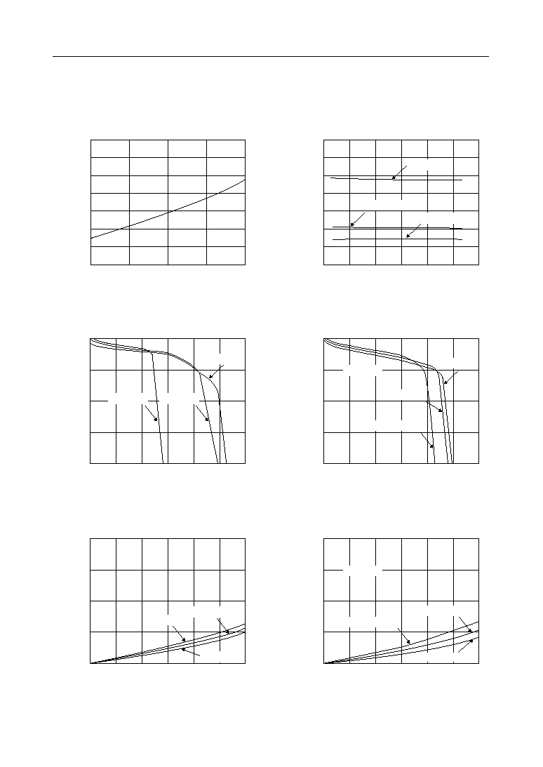
OPERATING CHARACTERISTICS
14
12
10
8
6
4
2
0
2
3
4
5
6
No-load circuit current [mA]
Power Supply Voltage
vs.
No-Load Circuit Current
Power supply [V]
14
12
10
8
6
4
2
0
≠50
0
25
50
100
No-load circuit current [mA]
No-Load Circuit Current
vs.
Temperature Characteristic
Temperature [∞C]
≠25
75
0
≠0.5
≠1
≠1.5
≠2
0
20
30
40
60
Output "H" voltage V
CC
≠V
OH
[V]
Output "H" Voltage Characteristic
Output current [mA]
10
50
0
20
30
40
60
Output "H" voltage V
CC
≠V
OH
[V]
Output "H" Voltage
vs.
Temperature Characteristic
Output current [mA]
10
50
0
≠0.5
≠1
≠1.5
≠2
2
1.5
1
0.5
0
0
20
30
40
60
Output "L" voltage V
OL
[V]
Output "L" Voltage Characteristic
Output current [mA]
10
50
0
20
30
40
60
Output "L" voltage V
OL
[V]
Output "L" Voltage
vs.
Temperature Characteristic
Output current [mA]
10
50
2
1.5
1
0.5
0
V
CC
=6 V
V
CC
=3 V
V
CC
=2 V
V
CC
=2 V
V
CC
=3 V
V
CC
=6 V
Ta=≠40∞C
Ta=25∞C
Ta=85∞C
V
CC
=3 V
V
CC
=2 V
V
CC
=3 V
V
CC
=6 V
V
CC
=3 V
Ta=≠40∞C
Ta=25∞C
Ta=85∞C

13/16
MSA180
° Semiconductor
7
6
5
4
3
2
3
4
5
6
Voltage gain, A
V1
[Magnification]
Power Supply Voltage
vs.
Voltage Gain
Power Supply Voltage [V]
7
6
5
4
3
≠50
0
25
50
100
Voltage gain, A
V1
[Magnification]
Temperature [∞C]
≠25
75
120
100
60
20
≠20
0
2
3
4
6
MODE1 input current [µA]
MODE1 Input voltage
vs.
Input Current
MODE1 input voltage [V]
1
5
0
2
3
4
6
MODE2 input current [µA]
MODE2 Input Voltage
vs.
Input Current
MODE2 input voltage [V]
1
5
20
0
≠20
≠40
≠120
3
2.5
1.5
0.5
0
0
2
3
4
6
BASE pin output current [mA]
BASE Pin Output Current
vs.
Temperature Characteristic
BASE voltage [V]
1
5
80
40
0
≠60
≠80
≠100
2
1
Ta=85∞C
Ta=25∞C
Ta=≠40∞C
V
CC
=6 V
V
CC
=2 V
V
CC
=6 V
V
CC
=2 V
V
CC
=3 V
V
CC
=6 V
V
CC
=6 V
Ta=85∞C
Ta=25∞C
Ta=≠40∞C
Voltage Gain
vs.
Temperature Characteristics
V
CC
=3 V
14/16
MSA180
° Semiconductor
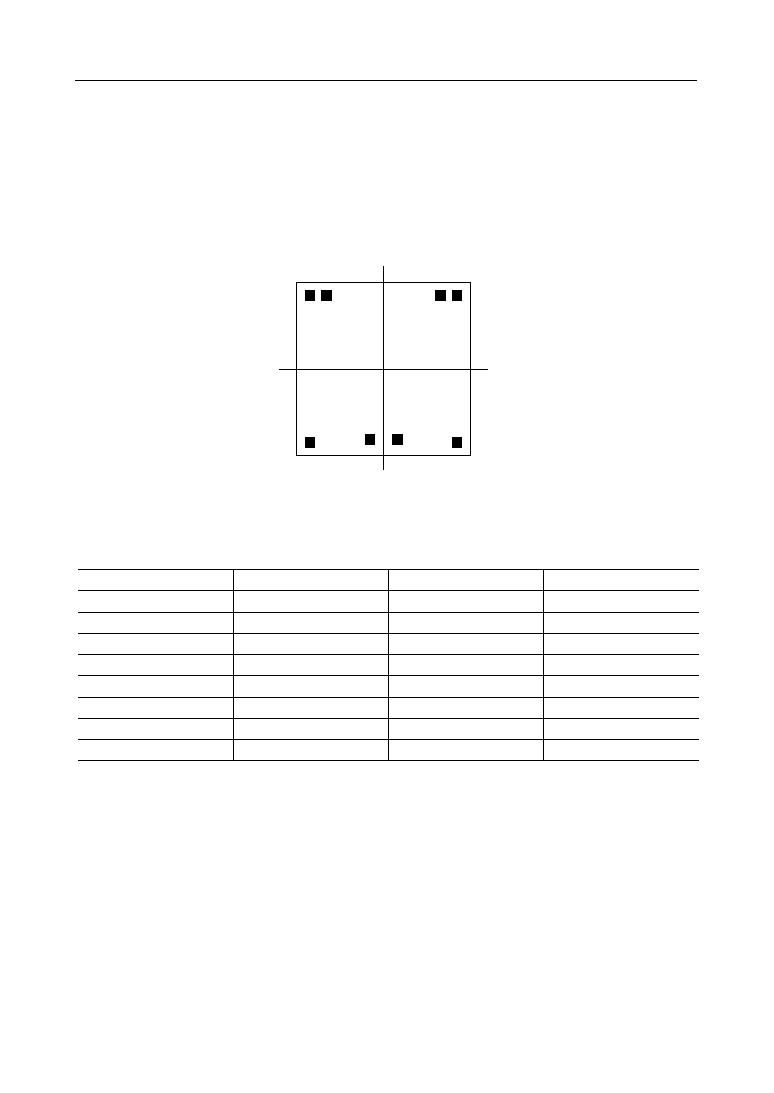
PAD CONFIGURATION
∑ Chip Layout
Chip size
:
2.00 mm • 2.00 mm
Chip thickness
:
350
µ
m
±
30
µ
m
Pad size
:
110
µ
m • 110
µ
m
Board potential
:
GND potential
2 1
8 7
3
6
4
5
Y-axis
X-axis
Pad Coordinates (Chip center: X=0, Y=0)
Pad name
X-coordinate [
mm]
Y-coordinate [
mm]
Pad
MODE2
≠655
835
1
A
IN
≠835
835
2
GND
≠835
≠835
3
SP
≠185
≠789
4
SP
121
≠789
5
V
CC
815
≠835
6
BASE
793
835
7
MODE1
613
835
8

15/16
MSA180
° Semiconductor
(Unit : mm)
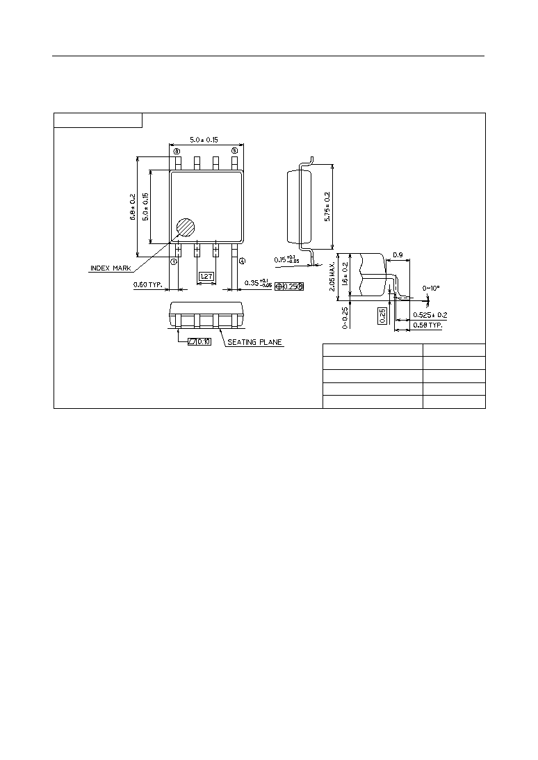
PACKAGE DIMENSIONS
DIP8-P-300-2.54
Package material
Lead frame material
Pin treatment
Solder plate thickness
Package weight (g)
Epoxy resin
42 alloy
Solder plating
5 mm or more
0.46 TYP.
16/16
MSA180
° Semiconductor
(Unit : mm)
Notes for Mounting the Surface Mount Type Package
The SOP, QFP, TSOP, TQFP, LQFP, SOJ, QFJ (PLCC), SHP, and BGA are surface mount type
packages, which are very susceptible to heat in reflow mounting and humidity absorbed in
storage. Therefore, before you perform reflow mounting, contact Oki's responsible sales person
on the product name, package name, pin number, package code and desired mounting conditions
(reflow method, temperature and times).
SOP8-P-250-1.27-K
Package material
Lead frame material
Pin treatment
Solder plate thickness
Package weight (g)
Epoxy resin
42 alloy
Solder plating
5 mm or more
0.10 TYP.
Mirror finish

NOTICE
1.
The information contained herein can change without notice owing to product and/or
technical improvements. Before using the product, please make sure that the information
being referred to is up-to-date.
2.
The outline of action and examples for application circuits described herein have been
chosen as an explanation for the standard action and performance of the product. When
planning to use the product, please ensure that the external conditions are reflected in the
actual circuit, assembly, and program designs.
3.
When designing your product, please use our product below the specified maximum
ratings and within the specified operating ranges including, but not limited to, operating
voltage, power dissipation, and operating temperature.
4.
Oki assumes no responsibility or liability whatsoever for any failure or unusual or
unexpected operation resulting from misuse, neglect, improper installation, repair, alteration
or accident, improper handling, or unusual physical or electrical stress including, but not
limited to, exposure to parameters beyond the specified maximum ratings or operation
outside the specified operating range.
5.
Neither indemnity against nor license of a third party's industrial and intellectual property
right, etc. is granted by us in connection with the use of the product and/or the information
and drawings contained herein. No responsibility is assumed by us for any infringement
of a third party's right which may result from the use thereof.
6.
The products listed in this document are intended for use in general electronics equipment
for commercial applications (e.g., office automation, communication equipment,
measurement equipment, consumer electronics, etc.). These products are not authorized
for use in any system or application that requires special or enhanced quality and reliability
characteristics nor in any system or application where the failure of such system or
application may result in the loss or damage of property, or death or injury to humans.
Such applications include, but are not limited to, traffic and automotive equipment, safety
devices, aerospace equipment, nuclear power control, medical equipment, and life-support
systems.
7.
Certain products in this document may need government approval before they can be
exported to particular countries. The purchaser assumes the responsibility of determining
the legality of export of these products and will take appropriate and necessary steps at their
own expense for these.
8.
No part of the contents cotained herein may be reprinted or reproduced without our prior
permission.
9.
MS-DOS is a registered trademark of Microsoft Corporation.
Copyright 1999 Oki Electric Industry Co., Ltd.
Printed in Japan
E2Y0002-29-11