 | –≠–ª–µ–∫—Ç—Ä–æ–Ω–Ω—ã–π –∫–æ–º–ø–æ–Ω–µ–Ω—Ç: MSC1208 | –°–∫–∞—á–∞—Ç—å:  PDF PDF  ZIP ZIP |

1/14
MSC1208
° Semiconductor
GENERAL DESCRIPTION
The MSC1208 is a Bi-CMOS display driver for 1/2-duty vacuum fluorescent display tube.
It consists of 58-bit shift registers, latch circuits, a 10-bit digital dimming circuit, 4 • 4 switch
matrix, and a keyscan circuit for 2-channel, 3-contact rotary switch. With these features, the
MSC1208 not only can display frequencies for audio systems used in automobile applications
and various information, but also can accept keyboard entry. Thus the front panel functions can
be carried out only by this IC.
Since the MSC1208 has the data parity check function and the self-check functions, inspection
at shipment and failure detection can easily be performed.
In addition, since the MSC1208 uses serial interfacing, only two signal lines, DATA ENABLE
and DATA I/O, are used for connection with a microcontroller.
FEATURES
∑ Power supply voltage
: V
DD
=8 to 18V (Built-in 5V-regulator for logic)
∑ Operating temperature range
: ≠40 to 85
∞
C
∑ Directly drives 23 segments
: I
OH
=≠8.8mA, Max. at V
OH
=V
DD
≠0.8V
∑ Built-in 4 • 4 switch matrix and key scan circuit for 2ch, 3-contact switching
∑ Built-in digital dimming circuit with 10-bit resolution
∑ Data parity check function
∑ Self-check function (segment ON/OFF at intervals of about 1 second in test mode)
∑ Built-in RC oscillator (capacitor is connected externally)
∑ Built-in power-on reset circuit
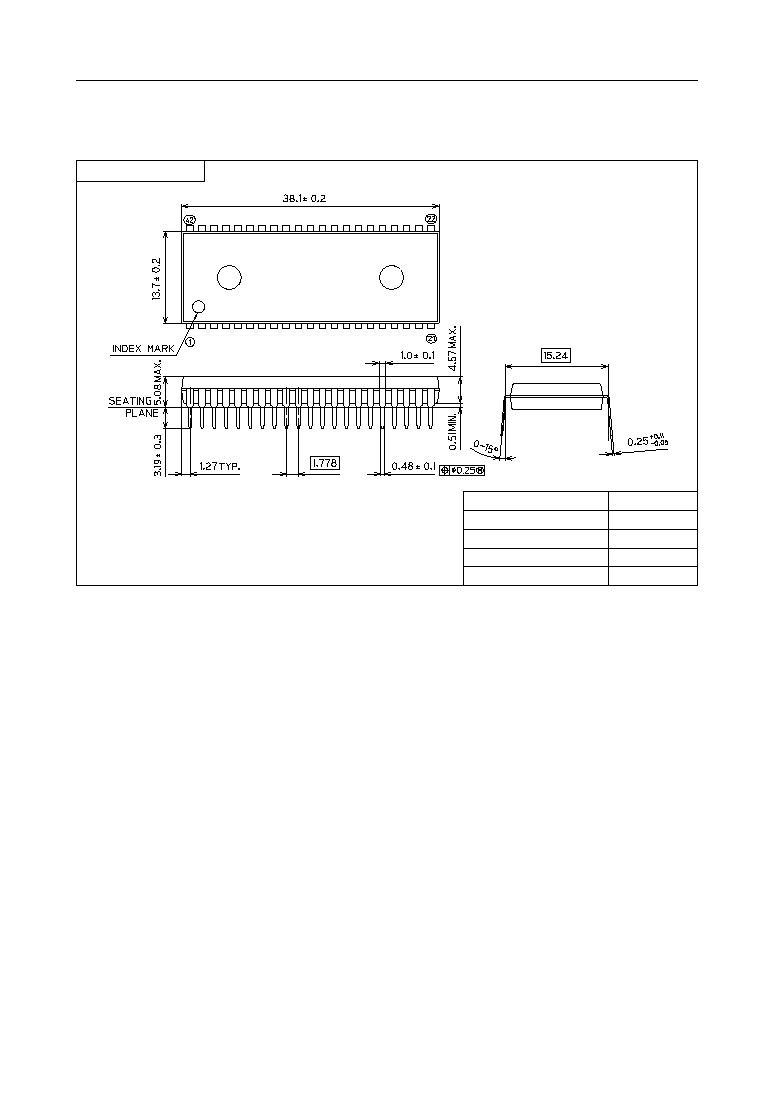
∑ Package:
42-pin plastic shrink DIP (SDIP42-P-600-1.78)
: (Product name : MSC1208SS)
••• indicates the code number.
° Semiconductor
MSC1208
23-bit
•
•
•
•
• 2 Duplex Controller/Driver with Digital Dimming and Keyscan Function
E2C0019-27-Y5
This version: Nov. 1997
Previous version: Jul. 1996
2/14
MSC1208
° Semiconductor
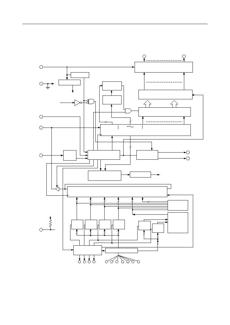
BLOCK DIAGRAM
GRID1
GRID2
V
DD
GND
DATA ENABLE
DATAI/O
PWMOUT
5V
SEG1
SEG23
46
∆23 Segment Control
Segment Driver
POR
Regulator
bit 46 to 24
(Grid2)
bit 23 to 1
(Grid1)
46 bit Latch
L
D
bit46
C
bit1
Display data
R
bit47
bit56
bit58, 57
Dimming data
58 bit Shift Register
bit56 to 1
Parity
Checker
Parity
Generator
SI
C
S
S
S
PE
out
58-bit Shift Register (26-bit presetable+32-bit
•"1")
S
S
S
L
4
4
4-bit
Latch
L
4
4
4-bit
Latch
L
4
4
4-bit
Latch
L
4
4
4-bit
Latch
8
2
L
3-bit
Latch
3
3
OSC
Grid
Pre-driver
OSC
Detector w/debounce
Row 4 3 2 1
Col 7 6 5 4 3 2 1
With100k
W pull-up resistor
Timing Generator
PWM
10-bit Presetable
Down Counter
TEST
Vreg
to PWM OUT
Parity
Parity
Generator
56
56
2
bit56 to 47
L
3-bit
Latch
Col1 to 3
Rotary
Direction
Checker &
Up/down
Counter
Col4 to 7
Timing
Generator

3/14
MSC1208
° Semiconductor
PIN CONFIGURATION (TOP VIEW)
SEG18 1
V
DD
42
SEG19 2
SEG17
41
SEG20 3
SEG16
40
SEG21 4
SEG15
39
SEG22 5
SEG14
38
SEG23 6
SEG13
37
ROW1 7
SEG12
36
ROW2 8
SEG11
35
ROW3 9
SEG10
34
ROW4 10
SEG9
33
COL1 11
SEG8
32
COL2 12
SEG7
31
COL3 13
SEG6
30
COL4 14
SEG5
29
COL5 15
SEG4
28
COL6 16
SEG3
27
COL7 17
SEG2
26
DATA ENABLE 18
SEG1
25
DATAI/O 19
GRID2
24
GND 20
GRID1
23
OSC 21
TEST
22
42-Pin Plastic Shrink DIP

4/14
MSC1208
° Semiconductor
PIN DESCRIPTIONS
Pin
Symbol
Type
42
V
DD
--
Power Sypply Voltage. A 12V power supply is connected.
Description
20
GND
--
19
Ground. 0V is applied.
Serial data input-output.
Enters the input mode when a "H" level signal is input to DATA ENABLE; enters the
output mode when a "L" level signal is input to DATA ENABLE.
DATA
DATA
ENABLE
I/O
18
I
Serial clock input.
During the "H" level of clock pulse, the input data of the DATA I/O pin (display data or
dimming data) is read, and during the "L" level of clock pulse, the output data (key
swich data) is output to the DATA I/O pin.
Input for the key matrix.
These pins are "L" active. When these keys are in the inactive state, these pins are at
"H" level through the internal pull-up resistors. COL1 to COL3 are for the rotary switch
and COL4 to COL7 are for the push-button switch.
11 to 17
COL1 to 7
I
7 to 10
ROW1 to 4
O
Signal outputs for scanning key matrix.
Normally, ROW1 to ROW4 output a "I" level. Key scanning is executed only once when
a transfer of the rotary switch contact or pressing down or release of the push-button
switch is detected. Key scanning is continued if the rotary switch contact is in the open
state after this one-time scanning. Then, scanning stops when the rotary switch contact
makes connection with any of the selective contacts. After key scanning is stopped,
ROW1 to ROW4 return to a "L" level.
21
OSC
I/O
RC oscillator connection. A capacitor is connected between GND and this pin.
25 to 41,
1 to 6
SEG1 to 23
O
Segment signal output.
Inverted GRID signal output. This signal is connected to an external grid driver
(e.g., PNP transistor) input.
Input for test. Since this pin has as internal a pull-up resistor, leave this pin open or
pull it up for use. When a "L" level signal is input, all segment outputs go on and off
at intervals of 1 second.
23 , 24
GRID1,2
O
22
TEST
I

5/14
MSC1208
° Semiconductor
ABSOLUTE MAXIMUM RATINGS
Power Dissipation
P
D
Ta=85∞C
400
Symbol
V
DD
Parameter
Power Supply Voltage
Condition
--
Rating
≠0.3 to+20
Unit
V
Input Voltage
Storage Temperature
V
IN
T
STG
--
≠0.3 to+6
≠55 to+150
∞C
--
V
mW
RECOMENDED OPERATING CONDITIONS
Symbol
V
DD
Parameter
Power Supply Voltage
Condition
--
Unit
V
T
op
Operating Temperature
--
∞C
Min.
8
≠40
Max.
18
85
"H" Input Voltage (1)
"H" Input Voltage (2)
"L" Input Voltage (1)
"L" Input Voltage (2)
Oscillation Frequency
V
IH1
DATA ENABLE, TEST
V
3.8
5.5
V
IH2
DATA I/O
V
4.0
5.5
V
IL1
DATA ENABLE, TEST
V
0
0.8
V
IL2
DATA I/O
V
0
1.2
f
OSC
C=68pF
kHz
256
768
Typ.
--
--
--
--
--
--
512
DATA ENABLE Frequency
DATA ENABLE Pulse Width
DATA ENABLE Rise Time
DATA ENABLE Fall Time
Data Delay Time
Input Data Valid Time
Output Data Valid Time
Frame Frequency
f
E
t
W
t
RE
t
FE
t
X
t
DV1
t
DV2
f
FR
Refer to Fig. 1
Refer to Fig. 1
Refer to Fig. 1
Refer to Fig. 1
Refer to Fig. 1
Refer to Fig. 1
Refer to Fig. 1
--
360
--
--
--
200
150
--
--
--
--
--
--
--
--
250
1.3
--
20
20
20
--
--
--
kHz
ms
ms
ms
ms
ms
ms
Hz
Refer to Fig. 3

6/14
MSC1208
° Semiconductor
ELECTRICAL CHARACTERISTICS
DC Characteristics
Symbol
V
IH1
Parameter
"H" Input Voltage
Condition
DATA ENABLE, TEST
Unit
V
V
IH2
"H" Input Voltage (2)
DATA I/O
V
Min.
3.8
4.0
Max.
--
--
"L" Input Voltage (1)
"L" Input Voltage (2)
"H" Input Current (1)
"L" Input Current (1)
V
IL1
DATA ENABLE, TEST
V
--
0.8
V
IL2
DATA I/O
V
--
1.2
I
IH1
V
IN
=5V, DATA ENABLE, DATA I/O
mA
≠5
5
I
IH2
V
IN
=5V, COL1 to 7, TEST
mA
≠30
30
I
IL1
V
IN
=0V, DATA ENABLE, DATA I/O
mA
≠5
5
I
IL2
V
IN
=0V,COL1 to 7, TEST
mA
≠15
≠160
V
OH1
I
OH1
=≠3mA, SEG1 to 17, V
DD
=13.8V
V
13
--
V
OH2
V
13
--
V
OL1
V
DD
=13.8V, All SEG pins
I
OL
=500
mA
I
OL
=200
mA
I
OL
=2
mA
V
V
V
--
--
--
2
1
0.3
"L" Input Current (2)
"H" Output Voltage (1)
"H" Output Voltage (2)
"L" Output Voltage (1)
"L" Output Voltage (2)
"L" Output Voltage (3)
"L" Output Voltage (4)
Current Consumption
V
OL2
V
OL3
V
OL4
I
DD
V
DD
=13.8V, I
OL
=10mA, GRID1,2
f
osc
=512kHz, No Load
--
--
--
--
V
0.8
V
0.8
V
1.2
mA
20
(Ta=≠40 to+85∞C,V
DD
=8 to 18V)
"H" Input Current (2)
I
OH2
=≠8mA, SEG18 to 23, V
DD
=13.8V
V
DD
=13.8V, I
OL
=200
mA, ROW1 to 4
V
DD
=13.8V, I
OL
=2mA, DATA I/O
AC Characteristics
Symbol
f
E
Parameter
DATA ENABLE Frequency
Condition
Refer to Fig. 1
Unit
kHz
t
W
DATA ENABLE Pulse Width
Refer to Fig. 1
ms
Min.
--
360
Max.
1.3
--
DATA ENABLE Rise Time
DATA ENABLE Fall Time
Data Delay Time
Input Data Valid Time
Output Data Valid Time
Output Data Active-to-High-Impedance
Time
t
RE
Refer to Fig. 1
ms
--
20
t
FE
Refer to Fig. 1
ms
--
20
t
X
Refer to Fig. 1
ms
--
20
t
DV1
Refer to Fig. 1
ms
200
--
t
DV2
Refer to Fig. 1
ms
150
--
t
HZ
Refer to Fig. 1
ms
--
5
(Ta=≠40 to+85∞C, V
DD
=8 to 18V)
Output Through Rate
(SEG, GRID)
DATA ENABLE Setup Time
Oscillation Frequency
t
SE
f
OSC
Refer to Fig. 2
C=68pF
ms
300
--
kHz
256
768
t
R
ms
--
5
C
L
=100pF, t=20 to 80%
or 80 to 20% of V
DD
Key Scan Characteristics
Symbol
t
KS
Parameter
Key Scan Time
Condition
Refer to Fig. 4
Unit
ms
t
SW
Key Scan Width
Refer to Fig. 4
ms
Min.
164
41
Max.
500
125
Typ.
250
62.5

7/14
MSC1208
° Semiconductor
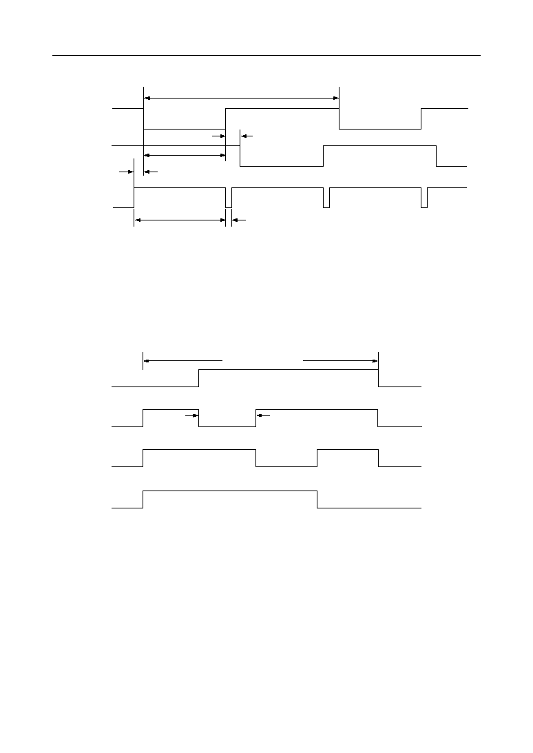
TIMING DIAGRAM
Hi-z
DATA I/O
(OUTPUT)
t
x
t
w
t
RE
t
x
VALID
Hi-z
DATA I/O
(INPUT)
DATA ENABLE
VALID
VALID
t
HZ
t
DV2
Hi-z
Hi-z
t
DV1
t
FE
t
w
f
E
Figure 1. Data Input-Output Timing
8V
DATA ENABLE
t
SE
V
DD
Figure 2. Power-ON Reset Timing
8/14
MSC1208
° Semiconductor
GRID1
GRID2
SEG1-23
1 Frame
2048-bit time (250Hz typ.)
8-bit time
1016-bit time max.
3-bit time
1019-bit time max.
5-bit time
Figure 3. SEG and GRID Output Timing
Note: 1. Shown above is the timing when the duty ratio of digital dimming is 1016/1024.
2. The grid and segment ON time is set by 10-bit digital dimming data.
3. 1-bit time=T
OSC
(=1/f
OSC
)=1.95 ms typ.
ROW1
ROW2
ROW3
Key Scan Time
Scan pulse width
ROW4
Figure 4. Key Scan Timing

9/14
MSC1208
° Semiconductor
FUNCTIONAL DESCRIPTION
Key Scan
In the case of the push-button switch, key scanning is started only when depression or release
of the key is detected for the purpose of minimizing noise caused by scanning signal. Then, after
completion of 1-cycle scanning, all the ROW outputs return to a "L" level.
The push-button switch input pins (COL4-COL7) are connected to a chattering absorption
circuit that absorbs chattering with the chattering time about 25ms (typ.), so input signals
shorter than 25ms are ignored. Because of this, key scanning is started about 25ms after key
input.
In the case of the rotary switch, key scanning is started only once when a transfer of the rotary
switch contact or pressing down or release of the push-button switch is detected. Key scanning
is continued if the rotary switch contact is in the open state after this one-time scanning. Then,
scanning stops when the rotary switch contact makes connection with any of the selective
contacts. After that, all "L" outputs return to a "L" level.
The rotary switch input pins (COL1-COL3) have an internal chattering absorption circuit that
absorbs chattering with the chattering time about 1ms (typ.), so input signals shorter than 1ms
are ignored. Because of this, key scanning is started about 1ms after a change in switch status.
The switch data is stored in the internal latch circuit, and then transferred to the output register
at the rising edge of the first pulse of DATA ENABLE.
The switch data consists of 16-push button switch data (S1-S16) and 2-rotary switch data (RS1
and RS2). The rotary switch data consists of 3 bits for contact-transfer count and 1-bit for
rotating direction. Since the maximum transfer count is "111" in binary, a transfer is counted up
to seven times. The rotating direction bit is "0" for the regular direction and "1" for the opposite
direction.
[Rotating direction]
Regular direction
: R11∆R12∆R13∆R11
Opposite direction : R13∆R12∆R11∆R13 (See figure below)
COL4
COL5
COL6
ROW1
ROW2
ROW3
ROW4
S1
S2
S3
S5
S6
S7
S9
S10
S11
S13
S14
S15
COL7
S4
S8
S12
S16
COL3
COL2
COL1
Figure 5. Key Matrix
ROW1
COL3
COL2
COL1
R11
R12
R13
Figure 6. Rotary Switch Section (RS1)

10/14
MSC1208
° Semiconductor
Digital Dimming
The segment and grid ON time can be controlled in the range of 0/1024 (=0%) to 1016/1024
(=99.2%) duty by 10-bit digital dimming data. (See Figure 3, "SEG and GRID Output Timing.")
Data Transfer
The input data (display data or dimming data) from DATA I/O is read into the internal register
after the DATA ENABLE input level changes from "L" to "H". The output data (key switch data)
is output to the DATA I/O pin after the DATA ENABLE input level changes from "H" to "L".
Using this method, bidirectional serial communication using two signal lines, DATA ENABLE
and DATA I/O, can be made.
The transfer data consists of 58 bits including 2-bit parity bit. Data transfer is completed if no
parity error occurs after the 58-bit data has been transferred to the internal register. If a parity
error occurs, the previously transferred data (display data or dimming data) is remained.
If an abnormality occurs in the DATA ENABLE line and no signal pulse is input for 10ms
±
5ms
or more, the data transfer is terminated even if it is in progress. Then, when the next pulse is
input, it is identified as the first pulse.
Diagnositc Function
1. Parity
Bit 57 and bit 58 (PO and PI) of the input data are used for parity check. For the output data,
parity is internally generated to add parity bit to bits 25 and 26.
The parity value is, for both input and output, "P0, P1=1, 1" when a total number of "1"s (or "0"s)
is even, and "P0, P1=0, 0" when it is odd.
2. Default mode
This device enters the default mode if no pulse is input to DATA ENABLE for about 1 second
or if a parity error keeps occurring for about 1 second.
In this mode, at the state of keeping the contents of the dimming data before entering the default
mode, the two segment outputs (SEG1, SEG2) only go ON.
This state is reset if no parity error is detected after the data has been transferred.
3. Self test
When the TEST pin is set to a "L" level, all segment outputs go on and off at intervals of about
1 second. At this time, the duty ratio for both segment and grid outputs becomes the maximum
(99.2%).
Power-On Reset
When power is turned on, this device is initialized by the internal power-on reset circuit. Then,
about 1second after the initialization, the device enters the default mode. At this time, the SEG1
and SEG2 segments go ON with the maximum duty ratio (99.2%). This state is reset if no parity
error is detected after the data has been transferred.

11/14
MSC1208
° Semiconductor
Input-Output Configuration
1. Input data (58 bits)
58
Bit
First in
PARITY
DATA
P1
57
P0
56
10
46
46
45
45
to
to
2
2
1
1
55
9
48
2
47
1
to
to
Dimming DATA
Display DATA
[Correspondence between input data (Display data) and SEG, GRID]
1 to 23
SEG1 to SEG23
Display DATA
24 to 26
SEG1 to SEG23
GRID1
GRID2
SEG NO.
GRID NO.
[Correspondence between dimming data and duty]
Dimming DATA
(LSB) 1 2 3 4 5 6 7 8 9 10 (MSB)
Duty (%)
0 0 0 0 0 0 0 0 0 0
to
0 0 0 1 1 1 1 1 1 1
to
1 1 1 1 1 1 1 1 1 1
0
to
99.2
* For dimming data greater than or equal to 0001111111, the duty is 99.2%.
(LSB)
(MSB)
[Parity]
When the total number of "1"s or "0"s in the display data and dimming data is even,
add "P0, P1=1, 1" to input data, and when it is odd, add "P0, P1=0, 0".
2. Output data (58 bits)
58 to 27
Bit
First out
ALL"1"
DATA
ALL"1"
26
P1
7
Q22
6
Q21
4
Q13
3
Q12
25
P0
8
Q23
24 to 9
S16 to S1
RS2 DATA
RS1 DATA
PARITY
16 SWITCHES
2
Q11
1
D1
5
D2
[Direction bit (Rotary switch rotating direction)]
D1, D2=Regular direction: 0, Opposite direction: 1
[Contact transfer count (rotary switch)]
Q11(LSB) to 13(MSB), Q21(LSB) to 23(MSB)
[Push-butter switch]
DS1 to S16=Pressing switch down: 1, Release: 0
[Parity]
When the total number of "1"s or "0"s in the key switch data is even, "P0, P1=1, 1" is
added to the output, and when it is odd, "P0, P1=0, 0" is added.
Note: "1" is output to every bit from bit 27 to bit 58.
12/14
MSC1208
° Semiconductor
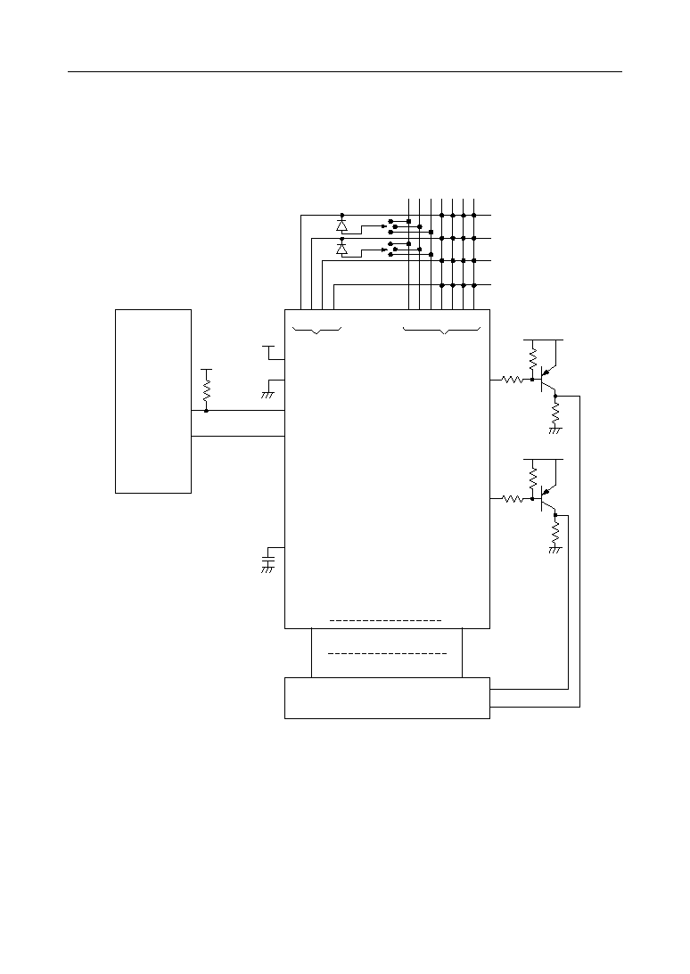
APPLICATION CIRCUITS
Example of a Basic Application Circuit
SEG1
SEG23
1
3
V
DD
GRID1
GRID2
GND
DATA I/O
DATA ENABLE
OSC
MSC1208
1/2-duty VF display tube
1 2 3
5
7
12V
ROW
COL
5V
12V
12V
TEST
4
2
4
6
RS1
RS2
*(Note)
Microcomputer
Note: Connect a diode between the rotary switch common contact and selective contacts, as
shown in the diagram above.
13/14
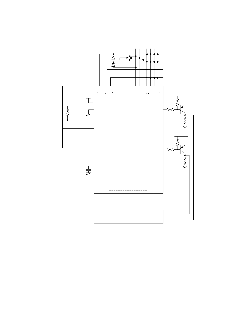
MSC1208
° Semiconductor
Example of Using a Single Rotary Switch
SEG1
SEG23
1
3
V
DD
GRID1
GRID2
GND
DATA I/O
DATA ENABLE
OSC
MSC1208
1/2-duty VF display Tube
1 2 3
5
7
12V
ROW
COL
5V
12V
12V
TEST
4
2
4
6
RS1
* (Note)
Microcomputer
Note: When using a sigle rotary switch, connect the ROW that is not used (ROW1 or ROW2)
and one of COL1 to COL3 via a diode.
If no rotary switch is used, connect ROW1 and one of COL1 to COL3 via a diode, and
also connect ROW2 and one of COL1 to COL3 via a diode.
14/14
MSC1208
° Semiconductor
(Unit : mm)
PACKAGE DIMENSIONS
Notes for Mounting the Surface Mount Type Package
The SOP, QFP, TSOP, SOJ, QFJ (PLCC), SHP and BGA are surface mount type packages, which
are very susceptible to heat in reflow mounting and humidity absorbed in storage.
Therefore, before you perform reflow mounting, contact Oki's responsible sales person for the
product name, package name, pin number, package code and desired mounting conditions
(reflow method, temperature and times).
SDIP42-P-600-1.78
Package material
Lead frame material
Pin treatment
Solder plate thickness
Package weight (g)
Epoxy resin
42 alloy
Solder plating
5
mm or more
4.52 TYP.