1
Semiconductor
MSM534031E
DESCRIPTION
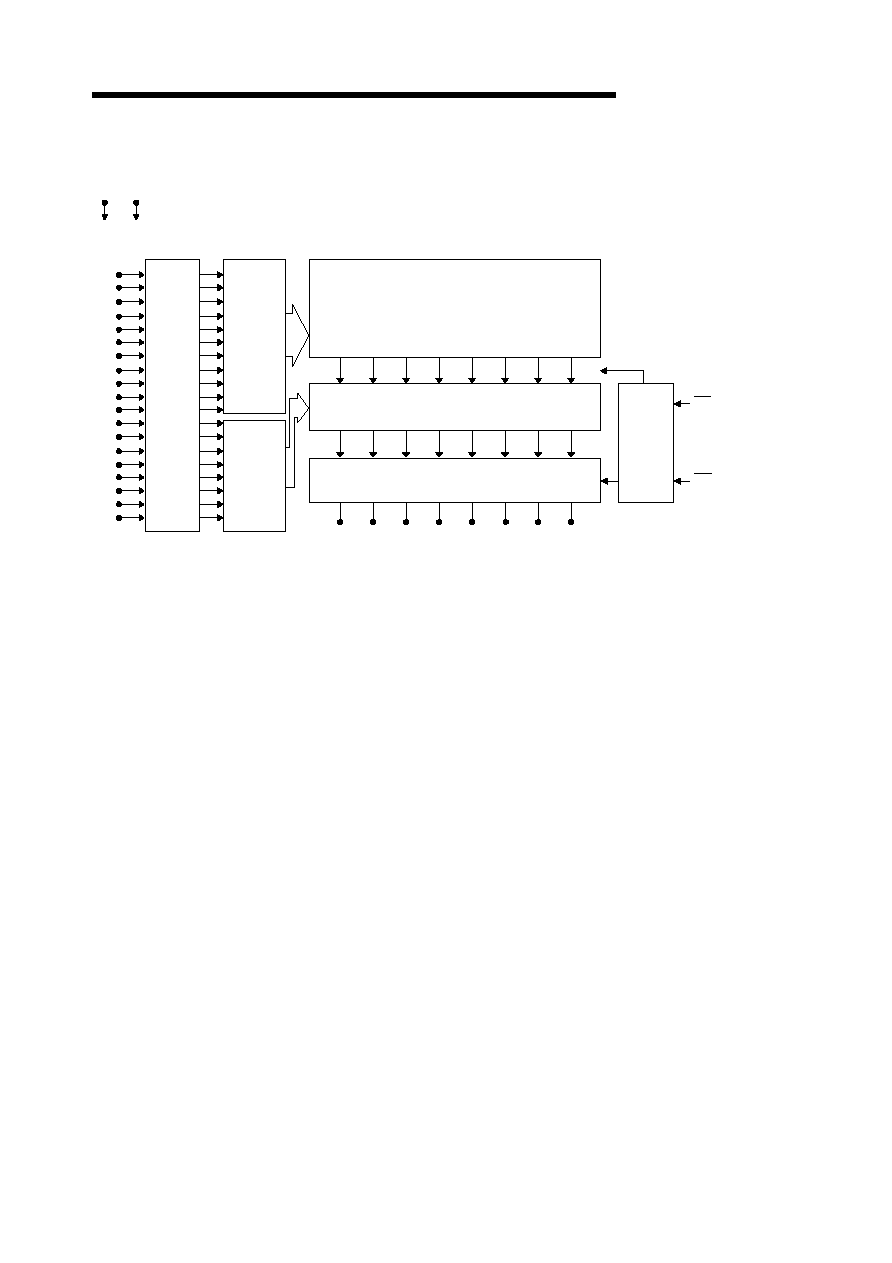
The OKI MSM534031E is a high-speed silicon gate CMOS Mask ROM with 524,288-word x
8-bit capacity. The MSM534031E operates on a single 3.0V or 3.3V power supply but offers
the same fast access times as products that operate at 5.0V. The MSM534031E's 8-bit wide
data path and pin compatibility with UV erasable EPROMs make it suited for use as large
capacity fixed memory for portable microcomputers and data terminals.
FEATURES
Single 3.0V or 3.3V power supply
524,288-words x 8-bit
Access time
--
current consumption
150ns
--
15mA (3.0V±0.3V operation)
120ns
--
20mA (3.3V±0.3V operation)
Tri-State output TTL compatible
Internal powerdown function
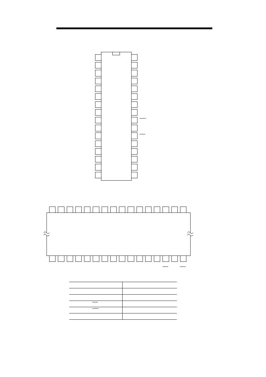
Packages:
32-PIN PLASTIC DIP (DIP32-P-600-2.54)
32-PIN PLASTIC SOP (SOP32-P-525-1.27-K)
32-PIN PLASTIC TSOP (TSOP32-P-814-0.80-K)
4MEPROM (32-PIN) pin compatible
524,288-Word x 8-Bit MASKROM
MSM534031E
4
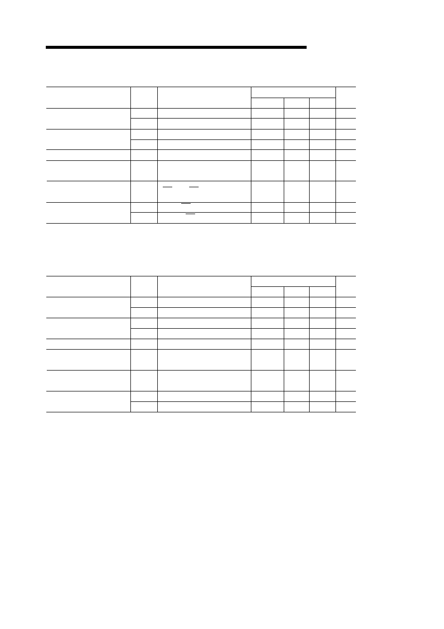
Recommended Operating Conditions (VCC=3.0V)
ELECTRICAL CHARACTERISTICS
Absolute Maximum Ratings
Operating Temperature
Storage Temperature
Power Supply Voltage
Input Voltage
Output Voltage
Power Dissipation
Parameter
Symbol
Unit
Conditions
Power Supply Voltage
"H" Input Voltage
"L" Input Voltage
Parameter
Symbol
Unit
3.3
Typ.
2.7
Conditions
V
V
V
W
to V
SS
Min.
Max.
3.0
V
0.0
0.0
0.0
V
2.0
3.0
V
0.6
0.0
V
Operating Temperature
70
0
Rated Value
6.0
Recommended Operating Conditions (VCC=3.3V)
Per Package T
opr
= 25∞C
0 to 70
≠55 to 150
≠0.3 to 7
≠0.3 to V
CC
+ 0.5
≠0.3 to V
CC
+ 0.5
1.0
Rating
∞C
∞C
T
opr
T
stg
V
CC
V
I
V
O
P
D
≠0.3
--
--
--
--
--
--
V
CC
V
SS
V
IH
V
IL
T
opr
Power Supply Voltage
"H" Input Voltage
"L" Input Voltage
Parameter
Symbol
Unit
3.6
Typ.
3.0
Conditions
Min.
Max.
3.3
V
0.0
0.0
0.0
V
2.0
3.3
V
0.6
0.0
V
Operating Temperature
70
0
Rated Value
6.0
≠0.3
--
--
--
--
--
--
V
CC
V
SS
V
IH
V
IL
T
opr
∞C
∞C
MSM534031E l
5
DC CHARACTERISTICS (VCC=3.0V±0.3V)
"H" Output Voltage
"L" Output Voltage
Parameter
Symbol
V
OH1
Unit
Typ.
Conditions
(Ta = 0 to 70∞C)
Min.
Max.
V
OH2
I
LI
I
LO
I
CC
I
CCSC
I
CCST
V
V
10
uA
20
mA
10
uA
50
uA
Input Leakage Current
Output Leakage Current
10
uA
l
DC CHARACTERISTICS (VCC=3.3V±0.3V)
Rated Value
V
OL1
0.1
V
OL2
V
0.4
V
CE = V
IL
,
OE = V
IH,
t
C
= 120
ns
CE = V
CC
≠0.2V
CE = V
IH MIN
I
OH
= ≠100uA
V
I
= 0 to V
CC
V
O
= 0 to V
CC
CE = V
IH MIN
I
OH
= ≠1.0mA
I
OL
= 100uA
I
OI
= 1.0mA
--
--
--
≠10
≠10
--
--
V
CC
≠ 0.1
V
CC
≠ 0.4
--
--
--
--
--
--
--
--
--
--
--
Power Supply Current
(Operating)
Power Supply Current
(Standby)
"H" Output Voltage
"L" Output Voltage
Parameter
Symbol
V
OH1
Unit
Typ.
Conditions
(Ta = 0 to 70∞C)
Min.
Max.
V
OH2
I
LI
I
LO
I
CC
I
CCSC
I
CCST
V
V
10
µA
15
mA
10
µA
50
µA
Input Leakage Current
Output Leakage Current
10
µA
Rated Value
V
OL1
0.1
V
OL2
V
0.4
V
CE =V
IL
,
OE =V
IH,
t
C
=150ns
CE = V
CC
≠0.2V
CE = V
IH MIN
I
OH
= ≠100µA
V
I
= 0 to V
CC
V
O
= 0 to V
CC
CE = V
IH MIN
I
OH
= ≠1.0mA
I
OL
= 100µA
I
OI
= 1.0mA
--
--
--
≠10
≠10
--
--
V
CC
≠ 0.1
V
CC
≠ 0.4
--
--
--
--
--
--
--
--
--
--
--
Power Supply Current
(Operating)
Power Supply Current
(Standby)