1
° Semiconductor
MSM6636
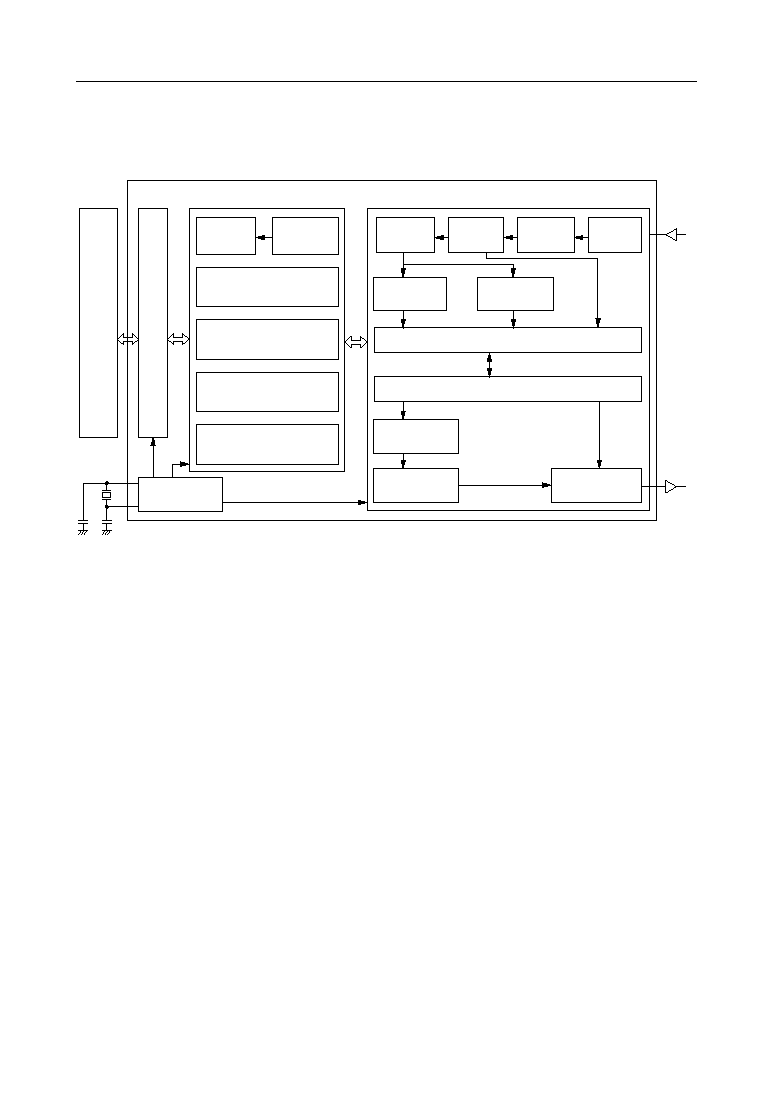
GENERAL DESCRIPTION
The MSM6636 is a transmission controller for automotive LAN based on data communication
protocol SAE-J1850. This LSI can realize a data bus topology bus LAN system with a PWM bit
encoding method (41.6 K bps). In addition to a protocol control circuit, MSM6636 has an enclosed
quartz oscillation circuit, host CPU interface (clock synchronous serial / UART), a transmit/
receive buffer, and a bus receiver circuit that decreases the burden on the host CPU.
FEATURES
∑ Based on SAE-J1850 CLASS B DATA COMMUNICATION NETWORK INTERFACE (issued
August 12, 1991)
∑ CSMA/CD (Carrier-sense multiple access with collision detection)
∑ Internal transmit buffer (1 frame) and receive buffer (2 frames)
∑ Bit encoding: PWM (Pulse Width Modulation)
∑ Transmission Speed: 41.6K bps
∑ Multi-address setting with physical addressing: 1 type / functional addressing: 15 types
∑ Address filter function by multi-addressing (broadcasting possible)
∑ Automatic retransmission function by arbitration loss and non ACK
∑ 3 types of in-frame response support:
q Single-byte response from a single recipient
w Multi-byte response from a single recipient (with CRC code)
e Single-byte response from multiple recipients (ID response as ACK)
∑ Error detection by cyclic redundancy check (CRC)
∑ Various communication error detections
∑ Dual-wire bus abnormality detection by internal bus receiver and fault tolerance function
∑ Host CPU interface is LSB first / serial, 4 modes supported
q Clock synchronous serial (no parity)
Normal mode: 8-bit data
MPC Mode:
8-bit data + MPC bit (1: address / 0: data select bit)
w UART (yes/no parity selectable)
Normal mode: 1 start bit + 8-bit data + (parity) + 1 stop bit
MPC mode:
1 start bit + 8-bit data + MPC bit + (parity) + 1 stop bit
∑ Sleep Function
Low current consumption mode by oscillation stop (IDS Max < 50
µ
A)
SLEEP / WAKE UP control from host CPU, WAKE UP via LAN bus
∑ Available package 18pin DIP, 18 pin QFJ (PLCC) and 24pin SOP.
° Semiconductor
MSM6636
SAE-J1850 Communication Protocol Conformity Transmission Controller for Automo-
tive LAN
3
° Semiconductor
MSM6636
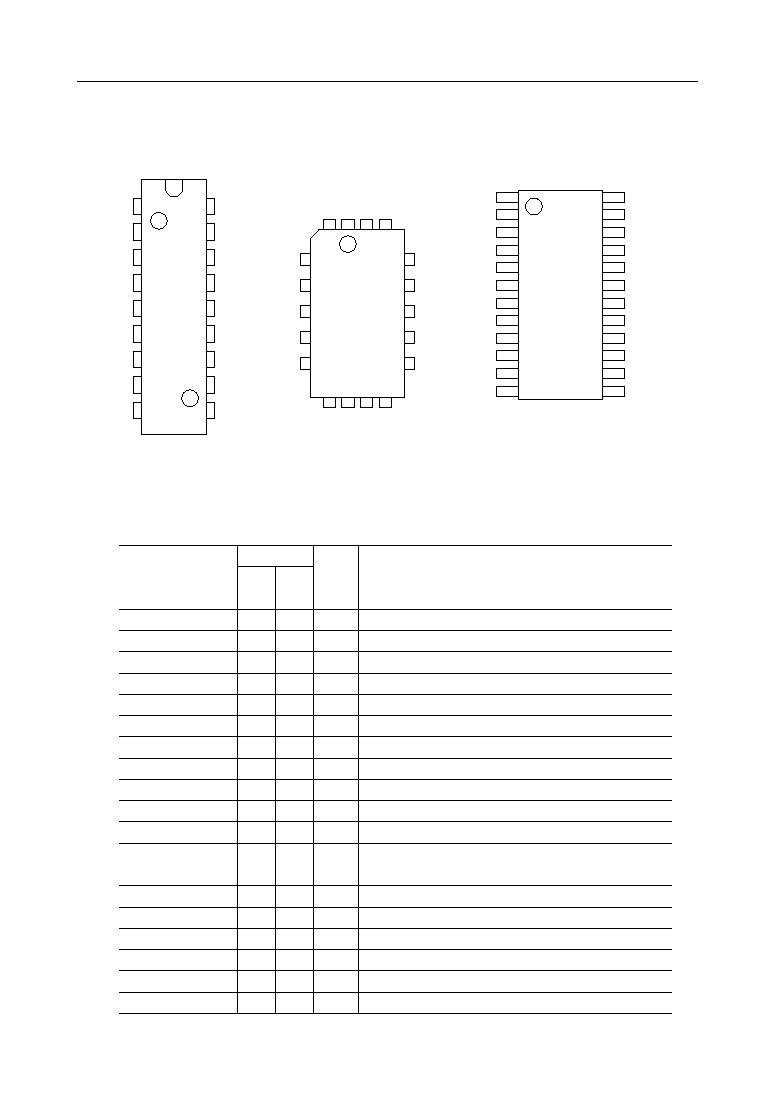
PIN CONFIGURATION (TOP VIEW)
PIN DESCRIPTION
Pin Name
I/O
Function
AVDD
1
--
Analog power supply pin
BO ≠
2
O
LAN - BUS output ≠
BI ≠
3
I
BI +
4
I
BO +
5
O
AGND
9
--
Analog ground pin
U - C
10
I
0: UART
1: clock synchronous serial select pin
M - N
11
I
0: MPC mode
1:normal mode select pin
DGND
12
--
Digital ground pin
OSC 1
13
O
Crystal oscillation output
OSC 0
14
I
Crystal oscillation input
A - D
15
I
0: data communication
1: address communication
SCLK / PAE
16
I
Serial clock input/Parity select pin
RXD
20
I
Serial data input pin
TXD
21
O
Serial data output pin
INT
22
O
Interrupt output pin
RES
23
I
Reset input pin
DVDD
24
--
Digital power supply pin
Pin #
1
2
3
4
5
6
7
8
9
10
11
12
13
14
15
16
17
18
DIP/
QFJ
SOP
LAN - BUS input ≠
LAN - BUS input +
LAN - BUS output +
18pin Plastic DIP
AVDD
DVDD
BO≠
RES
BI≠
INT
BI+
TXD
BO+
RXD
AGND
SCLK
/PAE
U-C
A-D
M-N
OSC0
DGND
OSC1
BI≠
INT
BI+
TXD
BO+
RXD
AGND
SCLK
/PAE
U-C
A-D
BO≠
M-N
AVDD
DGND
DVDD
OSC1
RES
OSC0
18pin Plastic QFJ
AVDD
DVDD
BO≠
RES
BI≠
INT
BI+
TXD
BO+
RXD
NC
NC
NC
NC
NC
NC
AGND
SCLK/PAE
U-C
A-D
M-N
OSC0
DGND
OSC1
24pin Plastic SOP
NC: No Connection
1
2
3
4
5
6
7
8
9
8
7
6
5
4
3
2
1
0
1
1
1
1
1
1
1
1
1
2
1
18 17
8
9
10 11
3
4
5
6
7
16
15
14
13
12
1
2
3
4
5
6
7
8
9
10
11
12
24
23
22
21
20
19
18
17
16
15
14
13

4
MSM6636
° Semiconductor
ABSOLUTE MAXIMUM RATINGS
Parameter
Symbol
Condition
Rated Value
Unit
Power Supply Voltage
DVDD, AVDD
-0.3~7.0
V
Input Voltage
V
I
-0.3~DVDD+0.3
V
Output Voltage
V
O
-0.3~DVDD+0.3
V
P
D(DIP)
*
1
Ta = 25∞C
860
mW
Storage Temperature
T
STG
-55~150
∞C
DGND = AGND = 0V
AVDD = DVDD
AVDD = DVDD
Power Dissipation
P
D(QFJ)
*
2
Ta = 25∞C
960
mW
P
D(SOP)
*
3
Ta = 25∞C
830
mW
P
D(DIP)*1
: 18PIN DIP package power dissipation
P
D(QFJ)*2
: 18PIN QFJ package power dissipation
P
D(SOP)*3
: 24PIN SOP package power dissipation
Power Dissipation Curve
1000
860
500
-40
25
125 150
Ambient temperature Ta (∞C)
Power dissipation P
D(DIP)
[mW]
1000
960
500
-40
25
125 150
Ambient temperature Ta (∞C)
Power dissipation P
D(QFJ)
[mW]
1000
830
500
-40
25
125 150
Ambient temperature Ta (∞C)
Power dissipation P
D(SOP)
[mW]
< 24PIN SOP package >
< 18PIN DIP package >
< 18PIN QFJ package >

5
° Semiconductor
MSM6636
OPERATION RANGE
Parameter
Symbol
Condition
Rated Value
Unit
Power Supply Voltage
DVDD, AVDD
AVDD = DVDD
4.5~5.5
V
Operating Frequency
f
OSC
DVDD = AVDD = 5V±10%
2~16
MHz
Operating Temperature
Ta
-40~+125
∞C
DGND = AGND = 0V
ELECTRICAL CHARACTERISTICS
DC Characteristics
H Level Input Voltage
V
IH1
--
A
DVDD • 0.8
--
DVDD + 0.3
V
Parameter
Symbol Condition Application
MIN
TYP
MAX
Unit
L Level Input Voltage
V
IL1
--
A
DGND - 0.3
--
DVDD • 0.2
V
H Level Input Current
I
IH1
V
I
= V
DD
B
--
--
+ 1
µA
L Level Input Current
I
IL1
V
I
= 0V
B
--
--
- 1
µA
H Level Input Current
I
IH2
V
I
= V
DD
C
--
--
+ 1
µA
L Level Input Current
I
IL2
V
I
= 0V
C
--
--
- 100
µA
H Level Input Current
I
IH3
V
I
= V
DD
BI (+)
--
--
+ 100
µA
L Level Input Current
I
IL3
V
I
= 0V
BI (-)
--
--
- 100
µA
H Level Output Voltage
V
OH1
I
O
= -400µA
D
DVDD - 0.4
--
--
V
L Level Output Voltage
V
OL1
I
O
= +3.2mA
D
--
--
DGND + 0.4
V
H Level Output Voltage
V
OH2
I
O
= -4.0mA
E
DVDD - 0.4
--
--
V
L Level Output Voltage
V
OL2
I
O
= +4.0mA
E
--
--
DGND + 0.4
V
Current Consumption 1
I
DS
During sleep
--
--
50
µA
Current Consumption 2
I
DD
f = 16MHz,
no load
--
--
10
mA
DVDD = AVDD = 5V±10%, DGND = AGND = 0V, Ta = -40 ~ +125∞C
H Level Input Voltage
V
IH2
--
F
DVDD - 2.0
--
DVDD + 1.0
V
L Level Input Voltage
V
IL2
--
F
DGND - 1.0
--
DGND + 2.0
V
Receiver Hysteresis Width
V
H
--
F
100
--
400
mV
GND Offset Voltage
V
OFF
--
--
±1
V
--
--
--
--
A: RES, SCLK/PAE, RXD, U-C, M-N, A-D, OSC0
B: SCLK/PAE, RXD, U-C, M-N, A-D
C: RES
D: TXD, INT
E: BO-, BO+
F: BI-, BI+