 | –≠–ª–µ–∫—Ç—Ä–æ–Ω–Ω—ã–π –∫–æ–º–ø–æ–Ω–µ–Ω—Ç: MSM9225B | –°–∫–∞—á–∞—Ç—å:  PDF PDF  ZIP ZIP |

FEDL9225B-03
1Semiconductor
This version: Aug. 2001
Previous version: Feb. 2001
MSM9225B
CAN (Controller Area Network) Controller
1/16
GENERAL DESCRIPTION
The MSM9225B is a microcontroller peripheral LSI which conforms to the CAN protocol for high-speed LANs
in automobiles.
FEATURES
∑
Conforms to CAN protocol specification (Bosch, V2.0 part B/Active)
∑
Maximum of 1 Mbps bit rate
∑
Communication method:
∑ Transmission line is bi-directional, two-wire serial communication
∑ NRZ (Non-Return to Zero) system using bit stuff function
∑ Multi-master system
∑ Broadcast system
∑
Message boxes:
∑ Up to 16 message boxes can be used, and messages up to 8 bytes long can be transmitted or received for
each message box.
∑ Number of received messages can be extended by group message function (up to 2 groups can be set)
∑ Overwrite flag is provided
∑
Priority control by identifier
∑ 2032 types in standard format, 2032
◊
2
18
types in extended format
∑
Microcontroller interface
∑ Corresponding to both parallel and serial interface
Parallel interface: Separate address/data bus type (with address latch signal/no address latch signal)
and multiplexed address/data bus type
Serial interface:
Synchronous communication type
∑ Three interrupt sources: Transmission/receive/error
∑
Error control:
∑ Bit error/stuff error/CRC error/form error/acknowledgment error detection functions
∑ Retransmission/error status monitoring function when error occurs
∑ Bit error flag/stuff error flag/CRC error flag/form error flag/acknowledge error flag are provided
∑
Communication control by remote data request function
∑
Sleep/Stop mode function
∑
Supply voltage: 5 V±10%
∑
Operating temperature: ≠40 to +125∞C
∑
Package:
44-pin plastic QFP (QFP44-P-910-0.80-2K) (Product name: MSM9225BGA-2K)
FEDL9225B-03
1Semiconductor
MSM9225B
2/16
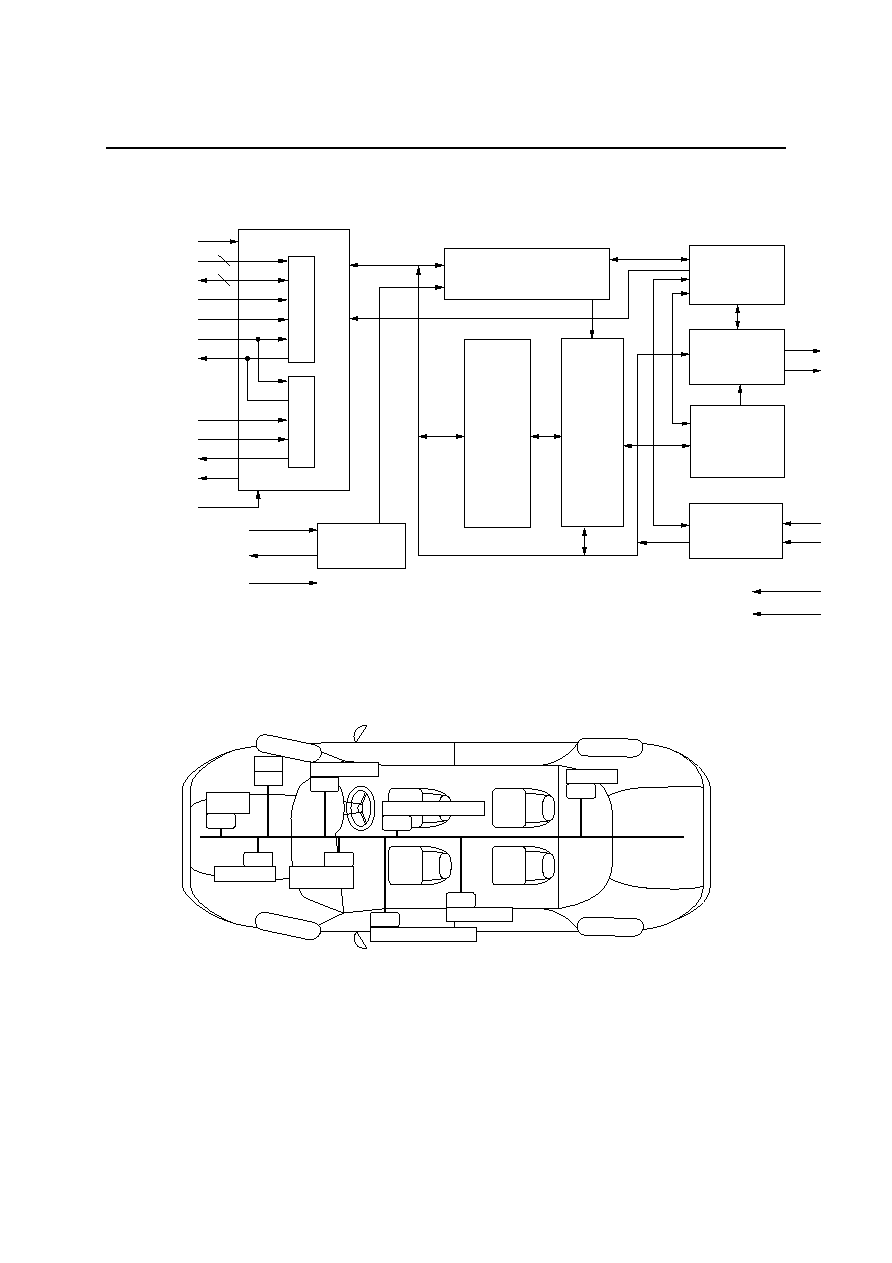
BLOCK DIAGRAM
Rx0
Tx0
Tx1
Rx1
V
DD
GND
Bit stream
logic
(BSL)
Transmission
control logic
(TCL)
Error
management
logic (EML)
Bit timing logic (BTL)
Message
memory
Control
register
Data
manage-
ment
logic
Receive
control logic
(RCL)
XT
XT
RESET
Timing
generator
m
i
cr
ocon
t
r
ol
ler
int
e
r
f
ace
8
Se
ri
a
l
I
/
F
P
a
r
a
llel
I/
F
A7-0
8
AD7-0/D7-0
PALE
PWR
PRD
W
/SR
PRDY/SWAIT
R
W
WAIT
SCLK
SDI
SDO
RD
RDY
Mode1, 0
CS
INT
CONFIGURATION EXAMPLE
CAN
ABS
Engine
controller
CAN
CAN
Transmission
Automatic
air conditioner
CAN
Seat-position controller
CAN
CAN
Outside mirror controller
CAN
Power window
Suspension
CAN
CAN Bus
Power steering
CAN

FEDL9225B-03
1Semiconductor
MSM9225B
3/16
PIN CONFIGURATION
33
32
31
30
29
28
27
26
25
24
23
1
2
3
4
5
6
7
8
9
10
11
A4
A5
A6
A7
SDO
GN
D
SDI
SCL
K
PR
D
W
/S
R
CS
IN
T
AD2
/
D2
AD1
/
D1
AD0
/
D0
M
ode1
M
ode0
GND
PA
L
E
PW
R
RES
E
T
V
DD
T1
X
34
35
36
37
38
39
40
41
42
43
44
A3
A2
A1
A0
V
DD
GND
AD7/D7
AD6/D6
AD5/D5
AD4/D4
AD3/D3
12
13
14
22
21
20
19
18
17
16
15
V
DD
XT
XT
GND
PRDY
/SWAIT
GND
R 0
X
R 1
X
V
DD
GND
T 0
X
44-Pin Plastic QFP (Top View)

FEDL9225B-03
1Semiconductor
MSM9225B
4/16
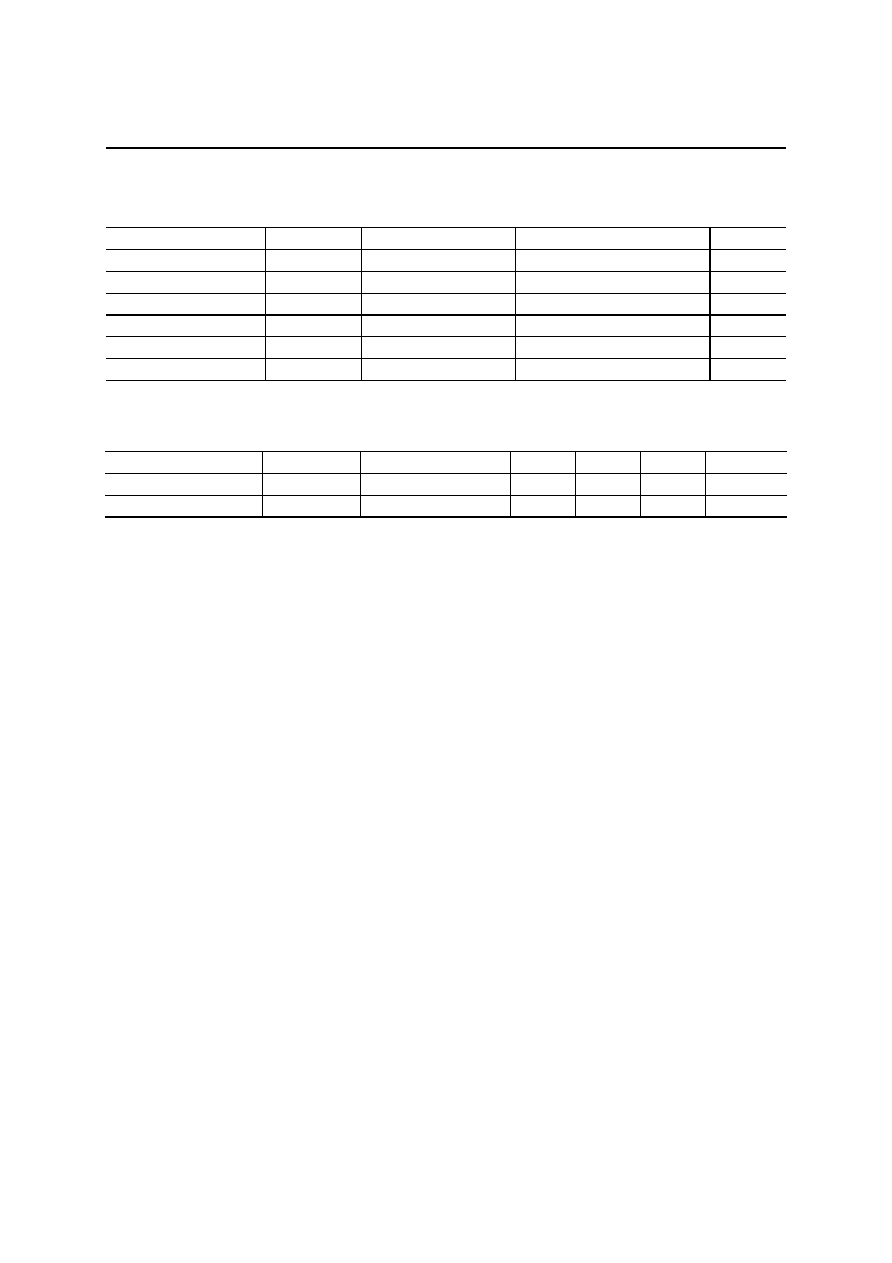
PIN DESCRIPTIONS
Symbol
Pin
Type
Description
CS
10
I
Chip select pin. When "L", PALE,
PWR
,
PRD
/SR
W
, SCLK and SDO
pins (microcontroller interface pins) are valid.
When "H", these pins are invalid.
A7-0
41-44, 1-4
I
Address bus pins (when using separate buses). If used with a
multiplexed bus or if used in the serial mode, fix these pins at "H" or "L"
levels.
AD7-0/
D7-0
31-38
I/O
Multiplexed bus: Address/data pins (AD7-0)
Separate buses: Data pins (D7-0)
If used in the serial mode, fix these pins at a "L" levels.
PWR
26
I
Write input pin if used in the parallel mode. Data is captured when this
pin is at a "L" level.
If used in the serial mode, fix this pin at a "L" level.
PRD
/
SR
W
9
I
Parallel mode: Read signal pin (
PRD
)
When at a "L" level, data is output from the data pins.
Serial mode: Read/write signal pin (SR
W
)
When at a "H" level, data is output from the SDO pin.
When at a "L" level, the SDO pin is at high impedance, and data is
captured beginning with the second byte of data input from the SDI pin.
PALE
27
I
Address latch signal pin
When at a "H" level, addresses are captured.
If used in the parallel mode and the address latch signal is unnecessary
or in the serial mode, fix this pin at a "H" or "L" level.
SDI
7
I
Serial data input pin
Addresses (1st byte) and data (beginning from the 2nd byte) are input to
this pin, LSB first. If used in the parallel mode, fix this pin at a "H" or "L"
level.
SDO
5
O
Serial data output pin
When the
CS
pin is at a "H" level, this pin is at high impedance. When
CS
is at a "L" level, data is output from this pin, LSB first.
If used in the parallel mode, fix this pin at a "H" or "L" level.
SCLK
8
I
Shift clock input pin for serial data
At the rising edge of the shift clock, SDI pin data is captured. At the
falling edge, data is output from the SDO pin.
PRDY
/
SWAIT
16
O
Ready output pin
When required by the MSM9225B, a signal may be output to extend the
bus cycle until the internal access is completed.
Internal access in
progress
After completion of
access
Parallel mode
(
PRDY
)
"L" level output
High impedance
output
Serial mode
(SWAIT)
"H" level output
"L" level output

FEDL9225B-03
1Semiconductor
MSM9225B
5/16
Symbol
Pin
Type
Description
Mode1, 0
29, 30
I
Microcontroller interface select pins
INT
11
O
Interrupt request output pin
When an interrupt request occurs, a "L" level is output. This pin
automatically outputs a "H" level after 32 Ts (T = 1/fosc).
Three types of interrupts share this pin: transmission complete, reception
complete, and error.
RESET
25
I
Reset pin
System is reset when this pin is at a "L" level.
XT
13
I
XT
14
O
Clock pins. If internal oscillator is used, connect a crystal (ceramic
resonator).
If external clock is used, input clock via XT pin. The
XT
pin should be left
open.
Rx0, Rx1
18, 19
I
Receive input pin. Differential amplifier included.
Tx0, Tx1
22, 23
O
Transmission output pin
V
DD
12, 20, 24, 40
--
Power supply pin
GND
6, 15, 17, 21,
28, 39
--
GND pin
Mode1
Mode0
Interface
0
0
No address latch signal
0
1
Separate
buses
With address latch signal
1
0
Parallel
mode
Multiplexed buses
1
1
Serial mode
FEDL9225B-03
1Semiconductor
MSM9225B
6/16
ABSOLUTE MAXIMUM RATINGS
Parameter
Symbol
Condition
Rating
Unit
Power Supply Voltage
V
DD
Ta = 25∞C
≠0.3 to
+7.0
V
Input Voltage
V
I
--
≠0.3 to
V
DD
+3.0
V
Output Voltage
V
O
--
≠0.3 to
V
DD
+3.0
V
Power Dissipation
P
D
Ta
25∞C
615
mW
Operating Temperature
T
OP
--
≠40 to
+125
∞C
Storage Temperature
T
STG
--
≠65 to
+150
∞C
RECOMMENDED OPERATING CONDITIONS
Parameter
Symbol
Condition
Min.
Typ.
Max.
Unit
Power Supply Voltage
V
DD
V
DD
= AV
DD
4.5
5.0
5.5
V
Operating Temperature
T
OP
--
≠40
+25
+125
∞C

FEDL9225B-03
1Semiconductor
MSM9225B
7/16
ELECTRICAL CHARACTERISTICS
DC Characteristics
(V
DD
= 4.5 to 5.5 V, Ta = ≠40 to +125∞C)
Parameter
Symbol
Applicable pin
Condition
Min.
Max.
Unit
"H" Input Voltage
V
IH
Applies to all inputs
--
0.8V
DD
V
DD
+0.3
V
"L" Input Voltage
V
IL
Applies to all inputs
--
≠0.3
+0.2 V
DD
V
I
IH1
XT
3
25
µA
"H" Input Current
I
IH2
Other inputs
V
I
= V
DD
≠1.0
+1.0
µA
I
IL1
XT
≠25
≠3
µA
"L" Input Current
I
IL2
Other input
V
I
= 0V
≠1.0
+1.0
µA
V
OH1
INT
,
PRDY
/SWAIT
I
OH1
= ≠80
µ
A
V
DD
≠1.0
--
V
"H" Output Voltage
V
OH2
AD7-0/D7-0
I
OH2
= ≠400
µ
A
V
DD
≠1.0
--
V
V
OL1
INT
,
PRDY
/SWAIT
I
OL1
= 1.6 mA
--
0.4
V
"L" Output Voltage
V
OL2
AD7-0/D7-0
I
OL2
= 3.2 mA
--
0.4
V
Output Leakage Current
I
IH1
PRDY
/SWAIT
AD7-0/D7-0
V
I
= V
DD
/0 V
≠1.0
+1.0
µA
Dynamic Supply Current
I
DD
--
f
OSC
= 16 MHz,
No Load
--
9
mA
--
SLEEP Mode
--
400
µA
Static Supply Current
I
DDS
--
STOP Mode
--
100
µA
Rx0, Rx1 Characteristics
Differencial input mode
(V
DD
= 4.5 to 5.5 V, Ta = ≠40 to
+125∞C)
Parameter
Symbol
Applicable pin
Condition
Min.
Max.
Unit
`dominant' Input Voltage
VRx0 (d)
Rx0
≠0.3
VRx1 ≠0.4
V
`recessive Input Voltage
VRx0 (r)
Rx0
VRx1 = 0.4 V
DD
to 0.6 V
DD
VRx1 +0.4
V
DD
+3
V
Input Leakage Current
I
LK
Rx0, Rx1
VR
X1
= V
DD
/0 V
≠1
+1
µA
Tx0, Tx1 Characteristics
(V
DD
= 4.5 to 5.5 V, Ta = ≠40 to
+125∞C)
Parameter
Symbol
Condition
Min.
Max.
Unit
"H" Output Voltage
V
OH
I
OH
= ≠3.0 mA
V
DD
≠0.4
--
V
"L" Output Voltage
V
OL
I
OL
= 10.0 mA
--
0.4
V

FEDL9225B-03
1Semiconductor
MSM9225B
8/16
AC Characteristics
Parallel mode
(V
DD
= 4.5 to 5.5 V, Ta = ≠40 to
+125∞C, f
OSC
= 16 MHz)
Parameter
Symbol
Condition
Min.
Max.
Unit
ALE Address Setup Time
t
AS
--
10
--
ns
ALE Address Hold Time
t
AH
--
10
--
ns
PRD
Output Data Delay Time
t
RDLY
--
--
60
*
1
ns
PRD
Output Data Hold Time
t
RDH
--
5
--
ns
ALE "H" Level Width
t
WALEH
--
16.5
--
ns
When
PRDY
is not
generated
4T
--
ns
Access Cycle
When
PRDY
is
generated
t
cyc
--
7T
--
ns
Address Hold Time from
PRD
t
RAH
--
0
--
ns
ALE Delay Time from
PRD
t
HRA
--
27
--
ns
PRD
"H" Level Width
t
WRDH
--
27
--
ns
PRDY
"L" Delay Time
t
ARLDLY
--
--
35
ns
PRDY
"L" Level Width
t
WRDYL
--
0
2.5T
ns
Data Output Delay Time from
PRDY
t
ARDDLY
--
--
35
ns
PWR
Hold Time from
PRDY
t
ARWDLY
--
10
--
ns
Input Data Setup Time
t
WDS
--
30
--
ns
Input Data Hold Time
t
WDH
--
4
--
ns
PRD
Delay Time
t
RS
--
10
--
ns
PWR
Delay Time
t
WS
--
10
--
ns
Address Hold Time from
PWR
t
WAH
--
10
--
ns
ALE Delay Time from
PWR
t
HWA
--
27
--
ns
PWR
"H" Level Width
t
WRH
--
40
--
ns
PWR
"L" Level Width
t
WRL
--
20
*
1
--
ns
CS
Delay Time from
PRD
t
HRC
--
0
--
ns
CS
Delay Time from
PWR
t
HWC
--
0
--
ns
T = 1/f
OSC
The values with *1 indicate those when
PRDY
is not generated.
The values with *1 when
PRDY
is generated are defined by "Data Output Delay Time from
PRDY
"
t
ARDDLY
and "
PWR
Hold Time from
PRDY
" t
ARWDLY
.

FEDL9225B-03
1Semiconductor
MSM9225B
9/16
Serial mode
(V
DD
= 4.5 to 5.5 V, Ta = ≠40 to
+125∞C, f
OSC
= 16 MHz)
Parameter
Symbol
Condition
Min.
Max.
Unit
CS
Setup Time
t
CS
--
10
--
ns
CS
Hold Time
t
CH
--
8T
--
ns
SCLK Cycle
t
CP
--
167
--
ns
SCLK Pulse Width
t
CW
--
83
--
ns
SDI Setup Time
t
DS
--
30
--
ns
SDI Hold Time
t
DH
--
5
--
ns
SDO Output Enable Time
t
CSODLY
--
--
30
ns
SDO Output Disable Time
t
CSZDLY
--
--
30
ns
SDO Output Delay Time
t
PD
--
--
30
ns
SR
W
Setup Time
t
RS
--
10
--
ns
SR
W
Hold Time
t
RH
--
0
--
ns
SWAIT Output Delay Time
t
SRDLY
--
--
2T
ns
SWAIT "H" Level Width
t
WRDY
--
--
6T
ns
Byte Delay
t
WAIT
--
8T
--
ns
T = 1/f
OSC
Other timing characteristics
(V
DD
= 4.5 to 5.5 V, Ta = ≠40 to
+125∞C)
Parameter
Symbol
Condition
Min.
Max.
Unit
System Clock Cycle
t
clkcy
--
62
--
ns
RESET
"H" Level Input Width
t
WRSTH
--
5
--
µs
RESET
"L" Level Input Width
t
WRSTL
--
5
--
µs
INT
"L" Level Output Width
t
WINTL
--
32T
--
ns
T = 1/f
OSC

FEDL9225B-03
1Semiconductor
MSM9225B
10/16
TIMING DIAGRAMS
Separate Bus Mode
Read access timing
t
cyc
t
RAH
t
WRDH
t
RDH
t
ARLDLY
t
WRDYL
t
RDLY
t
RS
t
HRC
CS
A7-0
AD7-0/
D7-0
PRD
/SR
W
PRDY
/SWAIT
t
ARDDLY
Note:
The
PRDY
signal may be output depending on the internal state of the MSM9225B.
Write access timing
t
cyc
t
WAH
t
WRH
t
WDS
t
ARLDLY
t
WRDYL
t
WRL
t
WS
t
HWC
CS
A7-0
AD7-0/
D7-0
PWR
PRDY
/SWAIT
t
WDH
t
ARWDLY
Note:
The
PRDY
signal may be output depending on the internal state of the MSM9225B.
FEDL9225B-03
1Semiconductor
MSM9225B
11/16
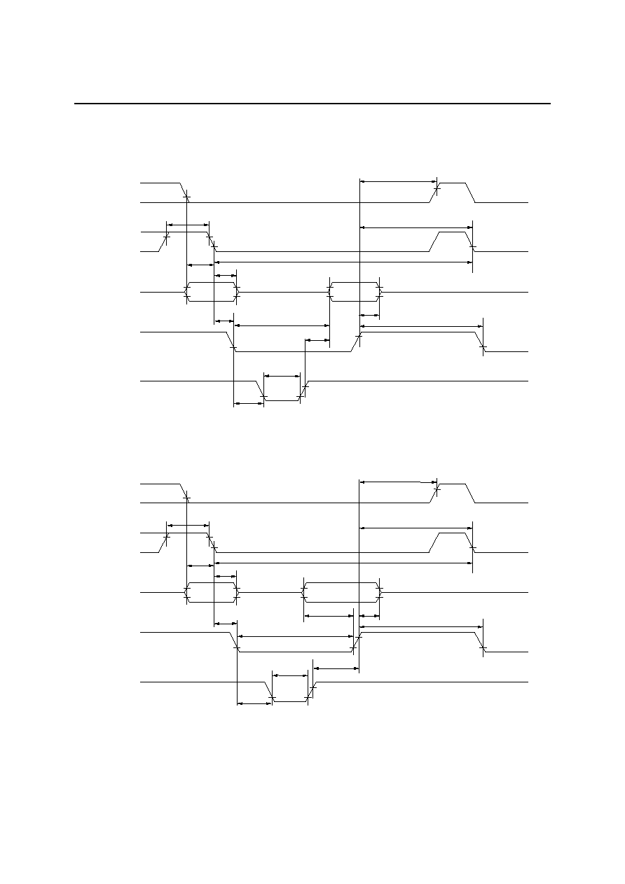
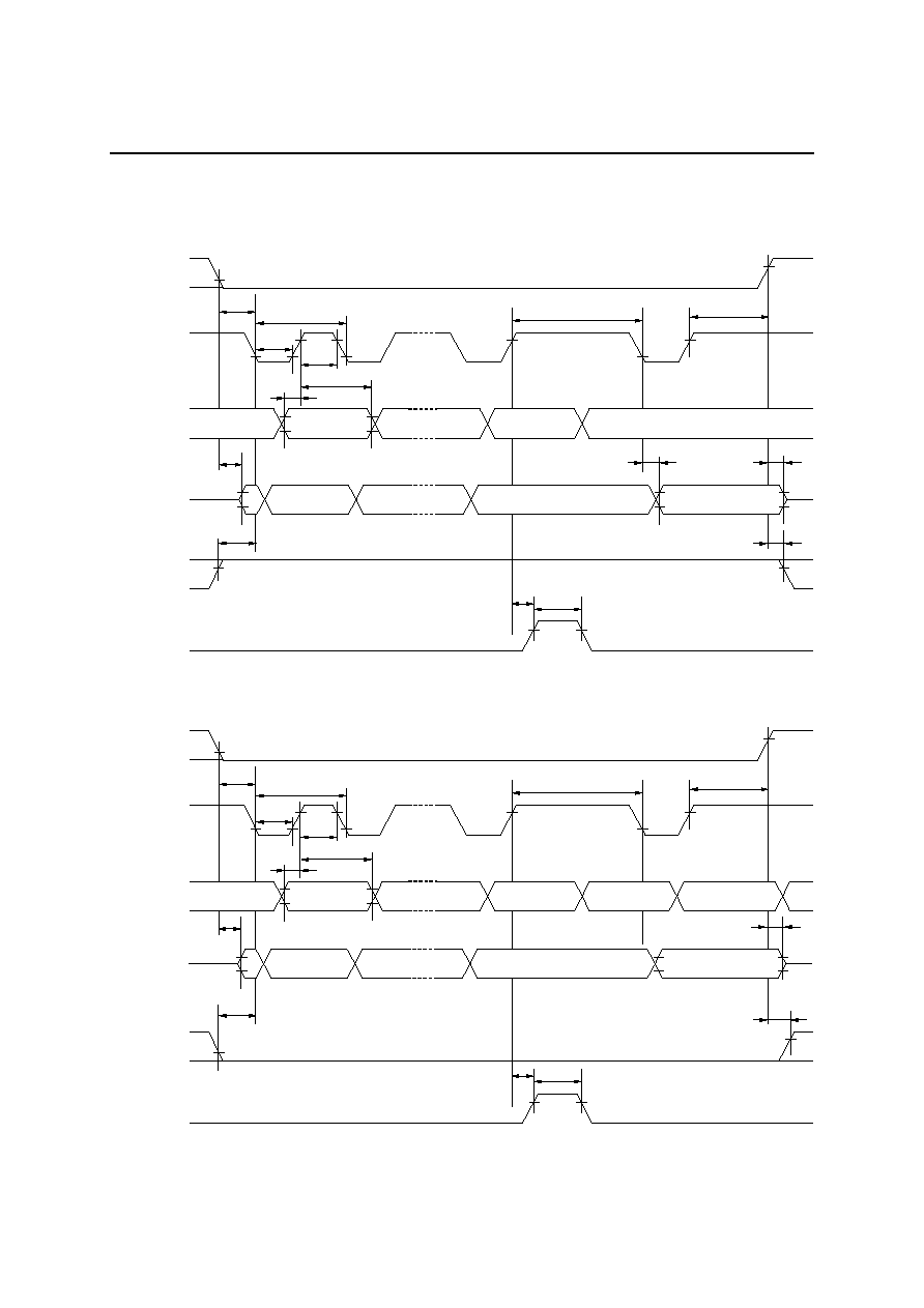
Separate Bus/Address Latch Mode
Read access timing
t
cyc
t
AH
t
WRDH
t
ARLDLY
t
WRDYL
t
RDLY
t
WALEH
t
HRC
CS
A7-0
AD7-0/
D7-0
PRD
/SR
W
PRDY
/SWAIT
t
RDH
t
HRA
t
AS
PALE
don't care
t
ARDDLY
t
RS
Note:
The
PRDY
signal may be output depending on the internal state of the MSM9225B.
Write access timing
t
cyc
t
AH
t
WRH
t
ARLDLY
t
WRDYL
t
WS
t
WALEH
t
HWC
CS
A7-0
AD7-0/
D7-0
PWR
PRDY
/SWAIT
t
WDS
t
HWA
t
AS
PALE
t
WRL
t
WDH
don't care
t
ARWDLY
Note:
The
PRDY
signal may be output depending on the internal state of the MSM9225B.
FEDL9225B-03
1Semiconductor
MSM9225B
12/16
Multiplexed Bus Mode
Read access timing
t
cyc
t
WRDH
t
ARLDLY
t
WRDYL
t
RDLY
t
WALEH
t
HRC
CS
AD7-0/
D7-0
PRD
/SR
W
PRDY
/SWAIT
t
RDH
t
HRA
t
AS
PALE
t
AH
t
ARDDLY
t
RS
Note:
The
PRDY
signal may be output depending on the internal state of the MSM9225B.
Write access timing
t
cyc
t
WRH
t
ARLDLY
t
WRDYL
t
WS
t
WALEH
t
HWC
CS
AD7-0/
D7-0
PWR
PRDY
/SWAIT
t
WDH
t
HWA
t
AS
PALE
t
AH
t
WDS
t
WRL
t
ARWDLY
Note:
The
PRDY
signal may be output depending on the internal state of the MSM9225B.
FEDL9225B-03
1Semiconductor
MSM9225B
13/16
Serial Mode
Read access timing
Note:
The SWAIT signal will be output during the interval between address and data transfers.
Write access timing
Note:
The SWAIT signal will be output during the interval between address and data transfers.
* : don't care
t
WRDY
CS
t
CS
t
CP
t
CW
t
CW
t
DH
t
DS
A0
A1
A6
A7
t
WAIT
Don't Care
t
CH
t
PD
t
CSZDLY
t
CSODLY
DMY0
DMY1
DMY6
DMY7
D0
t
RH
t
RS
t
SRDLY
SCLK
SDI
SDO
PRD
W
/SR
PRDY
/SWAIT
t
WRDY
CS
t
CS
t
CP
t
CW
t
CW
t
DH
t
DS
A0
A1
A6
A7
t
WAIT
t
CH
t
RH
t
RS
t
SRDLY
SCLK
SDI
PRD
W
/SR
PRDY
/SWAIT
D0
t
CSZDLY
t
CSODLY
*
*
*
*
*
SDO

FEDL9225B-03
1Semiconductor
MSM9225B
14/16
Other Timing
t
WRSTL
RESET
t
WRSTH
t
WINTL
INT
t
clkcy
CLK
(XT)
t
clkcy

FEDL9225B-03
1Semiconductor
MSM9225B
15/16
PACKAGE DIMENSIONS
(Unit: mm)
QFP44-P-910-0.80-2K
Mirror finish
Package material
Epoxy resin
Lead frame material
42 alloy
Pin treatment
Solder plating (
5µm)
Package weight (g)
0.41 TYP.
5
Rev. No./Last Revised
4/Nov. 28, 1996
Notes for Mounting the Surface Mount Type Package
The surface mount type packages are very susceptible to heat in reflow mounting and humidity
absorbed in storage. Therefore, before you perform reflow mounting, contact Oki's responsible sales
person on the product name, package name, pin number, package code and desired mounting
conditions (reflow method, temperature and times).

FEDL9225B-03
1Semiconductor
MSM9225B
16/16
NOTICE
1.
The information contained herein can change without notice owing to product and/or technical
improvements. Before using the product, please make sure that the information being referred to is up-to-
date.
2.
The outline of action and examples for application circuits described herein have been chosen as an
explanation for the standard action and performance of the product. When planning to use the product,
please ensure that the external conditions are reflected in the actual circuit, assembly, and program designs.
3.
When designing your product, please use our product below the specified maximum ratings and within the
specified operating ranges including, but not limited to, operating voltage, power dissipation, and operating
temperature.
4.
Oki assumes no responsibility or liability whatsoever for any failure or unusual or unexpected operation
resulting from misuse, neglect, improper installation, repair, alteration or accident, improper handling, or
unusual physical or electrical stress including, but not limited to, exposure to parameters beyond the
specified maximum ratings or operation outside the specified operating range.
5.
Neither indemnity against nor license of a third party's industrial and intellectual property right, etc. is
granted by us in connection with the use of the product and/or the information and drawings contained
herein. No responsibility is assumed by us for any infringement of a third party's right which may result
from the use thereof.
6.
The products listed in this document are intended for use in general electronics equipment for commercial
applications (e.g., office automation, communication equipment, measurement equipment, consumer
electronics, etc.). These products are not authorized for use in any system or application that requires
special or enhanced quality and reliability characteristics nor in any system or application where the failure
of such system or application may result in the loss or damage of property, or death or injury to humans.
Such applications include, but are not limited to, traffic and automotive equipment, safety devices,
aerospace equipment, nuclear power control, medical equipment, and life-support systems.
7.
Certain products in this document may need government approval before they can be exported to particular
countries. The purchaser assumes the responsibility of determining the legality of export of these products
and will take appropriate and necessary steps at their own expense for these.
8.
No part of the contents contained herein may be reprinted or reproduced without our prior permission.
Copyright 2001 Oki Electric Industry Co., Ltd.