©
Semiconductor Components Industries, LLC, 1999
December, 1999 ≠ Rev. 2
1
Publication Order Number:
1SMA10CAT3/D
1SMAXXCAT3 Series
Zener Transient
Voltage Suppressors
GENERAL DATA IS APPLICABLE TO ALL
SERIES IN THIS GROUP
Specification Features:
∑
Reverse Stand≠Off Voltage Range: 10 ≠ 78 V
∑
Bidirectional Operation
∑
Peak Power -- 400 Watts @ 1.0 ms
∑
ESD Rating of Class 3 (>16 kV) per Human Body Model
∑
Pico Seconds Response Time (0 V to BV)
∑
Flat Handling Surface for Accurate Placement
∑
Package Design for Top Side or Bottom Circuit Board Mounting
∑
Available in Tape and Reel
∑
Low Profile Package
Mechanical Characteristics:
CASE:
Void-free, transfer-molded plastic
FINISH:
All external surfaces are corrosion resistant with
readily solderable leads
POLARITY:
None
MOUNTING POSITION:
Any
MAXIMUM CASE TEMPERATURE FOR SOLDERING PURPOSES:
260
∞
C for 10 Seconds
MAXIMUM RATINGS
Rating
Symbol
Value
Unit
Peak Power Dissipation @ TL = 25
∞
C, PW = 10/1000
µ
s (Note 1)
Ppk
400
Watts
Thermal Resistance from Junction to Lead
R
JL
29
∞
C/W
Thermal Resistance from Junction to Ambient
R
JA
150
∞
C/W
Operating and Storage Junction Temperature Range
TJ, Tstg
150
∞
C
* FR4 Board, using ON Semiconductor minimum recommended footprint, as shown in case 403B outline dimensions spec.
NOTES: 1. Non≠repetitive current pulse.
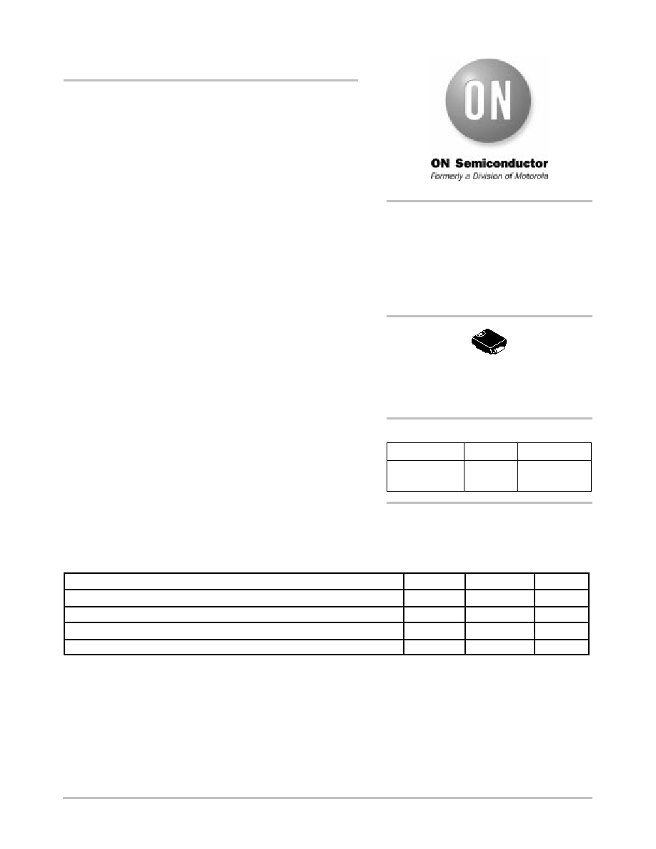
PLASTIC SURFACE MOUNT
BIDIRECTIONAL
ZENER OVERVOLTAGE
TRANSIENT SUPPRESSORS
10≠78 VOLTS VR
400 WATTS PEAK POWER
Devices listed in
bold, italic are ON Semiconductor
Preferred devices. Preferred devices are recommended
choices for future use and best overall value.
Device
Package
Shipping
ORDERING INFORMATION
1SMAXXCAT3
CASE 403B
Tape and Reel
5000 Units/Reel
SMA
PLASTIC
CASE 403B
http://onsemi.com

1SMAXXCAT3 Series
http://onsemi.com
3
RATING AND TYPICAL CHARACTERISTIC CURVES
TA = 25
∞
C
PW (ID) IS DEFINED AS THE
POINT WHERE THE PEAK CURRENT
DECAYS TO 50% OF Ipp.
= 10
µ
s
PEAK VALUE
Ippm
HALF VALUE ≠ Ipp/2
10/1000
µ
s WAVEFORM
AS DEFINED BY R.E.A.
td
120
100
80
60
40
0
0
1
2
3
4
20
5
Figure 1. Pulse Rating Curve
10≠4
100
0.1
1
10
10
1
0.1
tP, PULSE WIDTH (ms)
P
pk
NONREPETITIVE
PULSE WAVEFORM
SHOWN IN FIGURE 2.
TA = 25
∞
C
, PEAK POWER (kW)
0.01
0.001
Figure 2. Pulse Waveform
t, TIME (ms)
I ppm
, PEAK PULSE CURRENT
(%)
Figure 3. Pulse Derating Curve
120
100
80
60
40
0
0
40
80
120
160
TA, AMBIENT TEMPERATURE (
∞
C)
PEAK
PULSE
DERA
TING IN % OF
20
200
PEAK POWER OR CURRENT
10 x 1000 WAVEFORM
AS DEFINED BY R.E.A.
1SMAXXCAT3 Series
http://onsemi.com
4
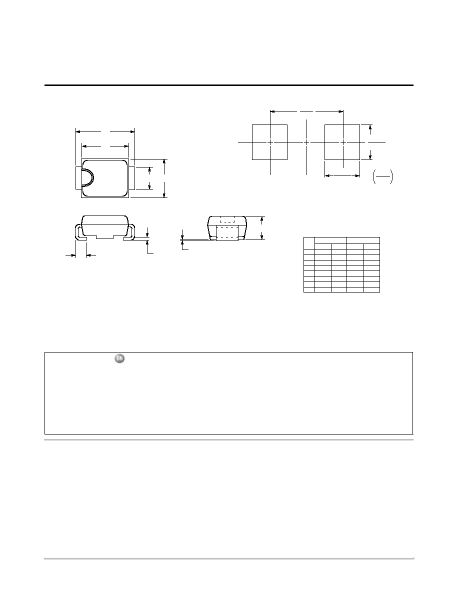
OUTLINE DIMENSIONS
400 Watt Peak Power
Transient Voltage Suppressors ≠ Surface Mounted
CASE 403B≠01
PLASTIC
(Refer to Section 10 of the TVS/Zener Data Book (DL150/D) for Surface Mount, Thermal Data and Footprint Information.)
NOTES:
1. DIMENSIONING AND TOLERANCING PER ANSI
Y14.5M, 1982.
2. CONTROLLING DIMENSION: INCH.
S
A
D
B
K
J
C
H
DIM
MIN
MAX
MIN
MAX
MILLIMETERS
INCHES
A
0.160
0.180
4.06
4.57
B
0.090
0.115
2.29
2.92
C
0.075
0.105
1.91
2.67
D
0.050
0.064
1.27
1.63
H
0.004
0.008
0.10
0.20
J
0.006
0.016
0.15
0.41
K
0.030
0.060
0.76
1.52
S
0.190
0.220
4.83
5.59
SMA
mm
inches
0.157
4.0
0.0787
2.0
0.0787
2.0
ON Semiconductor and are trademarks of Semiconductor Components Industries, LLC (SCILLC). SCILLC reserves the right to make changes
without further notice to any products herein. SCILLC makes no warranty, representation or guarantee regarding the suitability of its products for any particular
purpose, nor does SCILLC assume any liability arising out of the application or use of any product or circuit, and specifically disclaims any and all liability,
including without limitation special, consequential or incidental damages. "Typical" parameters which may be provided in SCILLC data sheets and/or
specifications can and do vary in different applications and actual performance may vary over time. All operating parameters, including "Typicals" must be
validated for each customer application by customer's technical experts. SCILLC does not convey any license under its patent rights nor the rights of others.
SCILLC products are not designed, intended, or authorized for use as components in systems intended for surgical implant into the body, or other applications
intended to support or sustain life, or for any other application in which the failure of the SCILLC product could create a situation where personal injury or
death may occur. Should Buyer purchase or use SCILLC products for any such unintended or unauthorized application, Buyer shall indemnify and hold
SCILLC and its officers, employees, subsidiaries, affiliates, and distributors harmless against all claims, costs, damages, and expenses, and reasonable
attorney fees arising out of, directly or indirectly, any claim of personal injury or death associated with such unintended or unauthorized use, even if such claim
alleges that SCILLC was negligent regarding the design or manufacture of the part. SCILLC is an Equal Opportunity/Affirmative Action Employer.
PUBLICATION ORDERING INFORMATION
ASIA/PACIFIC: LDC for ON Semiconductor ≠ Asia Support
Phone:
303≠675≠2121 (Tue≠Fri 9:00am to 1:00pm, Hong Kong Time)
Toll Free from Hong Kong 800≠4422≠3781
Email: ONlit≠asia@hibbertco.com
JAPAN: ON Semiconductor, Japan Customer Focus Center
4≠32≠1 Nishi≠Gotanda, Shinagawa≠ku, Tokyo, Japan 141≠8549
Phone: 81≠3≠5487≠8345
Email: r14153@onsemi.com
Fax Response Line:
303≠675≠2167
800≠344≠3810 Toll Free USA/Canada
ON Semiconductor Website: http://onsemi.com
For additional information, please contact your local
Sales Representative.
1N6267A/D
North America Literature Fulfillment:
Literature Distribution Center for ON Semiconductor
P.O. Box 5163, Denver, Colorado 80217 USA
Phone: 303≠675≠2175 or 800≠344≠3860 Toll Free USA/Canada
Fax: 303≠675≠2176 or 800≠344≠3867 Toll Free USA/Canada
Email: ONlit@hibbertco.com
N. American Technical Support: 800≠282≠9855 Toll Free USA/Canada
EUROPE: LDC for ON Semiconductor ≠ European Support
German Phone: (+1) 303≠308≠7140 (M≠F 2:30pm to 5:00pm Munich Time)
Email: ONlit≠german@hibbertco.com
French Phone: (+1) 303≠308≠7141 (M≠F 2:30pm to 5:00pm Toulouse Time)
Email: ONlit≠french@hibbertco.com
English Phone: (+1) 303≠308≠7142 (M≠F 1:30pm to 5:00pm UK Time)
Email: ONlit@hibbertco.com