 | –≠–ª–µ–∫—Ç—Ä–æ–Ω–Ω—ã–π –∫–æ–º–ø–æ–Ω–µ–Ω—Ç: CS2082 | –°–∫–∞—á–∞—Ç—å:  PDF PDF  ZIP ZIP |

©
Semiconductor Components Industries, LLC, 2001
July, 2001 ≠ Rev. 7
1
Publication Order Number:
CS2082/D
CS2082
Dual Airbag
Deployment ASIC
The CS2082 controls and monitors two airbag firing loops. The
independent firing loops are low≠ and high≠side controlled. Device
communication is through a Serial Peripheral Interface (SPI) port, and
includes frame error detection circuitry for data reliability.
Diagnostics include squib resistance measurement and continuous
monitoring for shorts to ground, shorts to battery, and for open loops.
The high≠ and low≠side drivers can be individually activated to
guarantee function and to identify shorts between firing loops.
Additional features include power on reset, overtemperature
protection, a charge pump, high≠side safing sensor closure detection,
an analog multiplexer, a monitor to ensure battery potential, and a
programmable monitor to ensure firing potential.
Features
∑
Serial Input Bus
∑
Two Squib Outputs
∑
Low≠ and High≠Side Control
∑
Monitors
≠
Squib Resistance
≠
Short to Ground or Battery
≠
Battery Potential
≠
Firing Potential
∑
Safing Sensor Detection
∑
60 V Peak Transient Voltage
http://onsemi.com
A
= Assembly Location
WL, L
= Wafer Lot
YY, Y
= Year
WW, W
= Work Week
PIN CONNECTIONS AND
MARKING DIAGRAM
Device
Package
Shipping
ORDERING INFORMATION
SO≠20L
37 Units/Rail
SO≠20L
1000 Tape & Reel
SO≠20L
DW SUFFIX
CASE 751D
CS2082EDW20
CS2082EDWR20
1
CS2082
A
W
L
YYWW
20
A
IN
D
OUT
FG2
FG1
SL2
SL1
SH2
SH1
VR2
VR1
D
IN
V
RES
V
CC
CHRG
GND
V
BAT
A
OUT
CLK
CS
MR
CS2082
http://onsemi.com
2
CS CLK D
IN
D
OUT
A
IN
A
OUT
MR
Battery
Monitor
V
RES
Monitor
Charge Pump
Monitor
Charge
Pump
Sensor
Monitor
+
≠
Diagnostic
+
≠
R
2R
R
V
BAT
1
2
Current
Limit
Gate
Drive
CHRG
1.5
Current
Limit
Gate
Drive
Current
Limit
Gate
Drive
Current
Limit
Gate
Drive
V
RES
1.5
CHRG
1.5
V
RES
1.5
V
BAT
V
BAT
10 k
10 k
10 k
10 k
CHRG
V
RES
VR1
SH1
SL1
FG1
SH2
SL2
FG2
V
CC
V
BAT
Overtemperature
Reset
V
CC
GND
VR2
+
≠
Current Limit
+
50 mV
V
BAT
V
CC
Resistive
Measurement
2
1
Analog
MUX
SPI
Figure 1. Block Diagram

CS2082
http://onsemi.com
3
MAXIMUM RATINGS*
Rating
Value
Unit
Storage Temperature
≠40 to 150
∞
C
V
BAT
≠0.3 to 24
V
V
RES
≠0.3 to 30
V
V
CC
≠0.3 to 6.0
V
ESD Susceptibility (Human Body Model)
500
V
Power Dissipation (Non≠Firing)
0.15
W
Power Dissipation (Both Firing Loops With Squibs Shorted)
140
W
Power Dissipation (Squib Resistance Measurement)
1.6
W
Peak Transient Voltage (46 V Load Dump @ 14 V V
BAT
)
60
V
Lead Temperature Soldering:
Reflow: (SMD styles only) (Note 1)
230 peak
∞
C
1. 60 second maximum above 183
∞
C.
*The maximum package power dissipation must be observed.
ELECTRICAL CHARACTERISTICS
(4.75 V < V
CC
< 5.25 V, 8.0 V < V
RES
< 30 V, 9.0 V < V
BAT
< 18 V,
≠40
∞
C < T
A
< +85
∞
C; unless otherwise stated.)
Parameter
Test Conditions
Min
Typ
Max
Unit
Supply Requirements
V
CC
Quiescent Current
V
CC
= 5.25 V
≠
2.0
4.0
mA
V
BAT
Quiescent Current
V
BAT
= 18 V
≠
2.5
5.0
mA
V
BAT
Measurement Current
V
BAT
= 18 V, R
SQUIB
= 1.0
≠
≠
80
mA
V
RES
Quiescent Current
V
RES
= 30 V
≠
≠
1.0
mA
V
RES
Firing Current
V
RES
= 30 V
≠
≠
3.0
mA
Power on Reset
V
BAT
= 9.0 V, V
RES
= 10 V
Power Reset Active Voltage
V
CC
Falling
3.50
4.00
4.25
V
Power Reset Off Voltage
V
CC
Rising
3.65
4.20
4.50
V
Hysteresis
≠
50
≠
≠
mV
Low Side Driver
V
RES
= 8.0 V = V
RX
, V
CC
= 5.0 V, V
BAT
= 8.0 V
Saturation Voltage
I = 1.2 A
≠
≠
1.8
V
Current Limit (I
LIMIT
)
V
SLX
≠ V
FGX
= 5.0 V
1.2
1.6
2.0
A
Turn≠on Delay Time
From CS falling Edge, I
D
= 0.9
◊
I
LIMIT(MIN)
≠
≠
75
µ
s
Turn≠off Delay Time
From CS falling Edge, I
D
= 0.1
◊
I
LIMIT(MIN)
≠
≠
25
µ
s
High Side Driver
V
RES
= 8.0 V = V
RX
, V
CC
= 5.0 V, V
BAT
= 8.0 V
Saturation Voltage
I = 1.2 A
≠
≠
1.8
V
Current Limit (I
LIMIT
)
V
RX
≠ V
SHX
= 5.0 V
1.2
2.0
2.5
A
V
R1
Quiescent Current Drivers off
V
RX
= V
RES
= 30 V
≠
≠
1.0
mA
V
R2
Quiescent Current Drivers off
V
RX
= V
RES
= 30 V
≠
≠
100
µ
A
Turn≠on Delay Time
From CS falling Edge, I
D
= 0.9
◊
I
LIMIT(MIN)
≠
≠
100
µ
s
Turn≠off Delay Time
From CS falling Edge, I
D
= 0.1
◊
I
LIMIT(MIN)
≠
≠
25
µ
s
Thermal Shut Down
Thermal Shutdown Temp
Guaranteed by Design
150
180
210
∞
C
Thermal Hysteresis
Guaranteed by Design
30
40
60
∞
C
CS2082
http://onsemi.com
4
ELECTRICAL CHARACTERISTICS (continued)
(4.75 V < V
CC
< 5.25 V, 8.0 V < V
RES
< 30 V, 9.0 V < V
BAT
< 18 V,
≠40
∞
C < T
A
< +85
∞
C; unless otherwise stated.)
Parameter
Unit
Max
Typ
Min
Test Conditions
Thermal Shut Down
Time to Thermal Shutdown
R
SQUIB
= 0, V
RX
= 30 V, T = 85
∞
C,
Guaranteed by Design
7.0
≠
≠
ms
Squib Resistive Measurements
V
CC
= 5.0 V, R
MR
= 49.9
W
, V
RES
= 30 V
Squib Differential Voltage
V
DIFF
= SHx ≠ SLx, R
SQUIB
= 1.0
to 10
46
53
60
mV
Difference Between SHx & MR
current ≠ SHx reference
I
SQUIB
= 50 mA
≠1.0
≠
1.0
%
SHx Current Limit
R
SQUIB
= 0
67
100
133
mA
SLx Current Limit
R
MR
= 0
77
115
153
mA
MR Voltage Clamp
≠
V
CC
≠ 0.3
≠
V
CC
+ 0.3
V
Turn On Delay Time excluding
external Capacitors
≠
≠
≠
100
µ
s
Turn off Delay Time
≠
≠
≠
50
µ
s
Short Measurements
V
CC
= 5.0 V, V
RES
.
V
BAT,
V
RX
.
V
BAT
SHx pull≠up resistance to V
BAT
SLx pull≠down resistance
V
BAT
= 18 V
4.0
4.0
10
10
17
17
k
k
Pull≠up resistor matching
≠
≠5.0
≠
5.0
%
Pull≠down resistor matching
≠
≠5.0
≠
5.0
%
Short to V
BAT
Trip
SHx short to Battery
SLx bit set to 1
0.73
◊
V
BAT
0.75
◊
V
BAT
0.77
◊
V
BAT
V
Short to GND Trip
SHx short to GND
SGx bit set to 1
0.23
◊
V
BAT
0.25
◊
V
BAT
0.27
◊
V
BAT
V
V
BAT
Monitoring
V
CC
= 5.0 V, External V
BAT
Diode not included, V
RES
= 30 V
V
BAT
Low Trip
BL bit set to 1 when below trip
7.5
8.5
9.5
V
V
BAT
High Trip
BL bit set to 0 when above trip
8.0
9.0
10
V
V
RES
Monitoring
V
CC
= 5.0 V, V
BAT
= 18 V
V
RES
Low Trip
$6d AUX register b0 = 0
15.7
17.5
19.3
V
V
RES
High Trip
$6d AUX register b0 = 0
16.5
18.5
20.5
V
V
RES
Low Trip
$6d AUX register b0 = 1
21.5
24.0
26.5
V
V
RES
High Trip
$6d AUX register b0 = 1
22.5
25
27.5
V
Safing Sensor Monitor
External Resistance Trip Range
SSC bit set when resistance is less
30
400
600
Charge Pump and Monitor
V
CC
= 5.0 V, V
BAT
= 10 V
Oscillator Frequency
V
RES
= 10 V
200
≠
800
kHz
Charge Pump charge time
C
CHG
= 0.1
µ
F, V
RES
= 8.0 V,
Chrg from 8.0 V to 14 V
≠
≠
20
ms
Charge Pump Low Voltage
CL bit set to 1 when below trip
14.5
16.0
17.5
V
Charge Pump High Voltage
CL bit set to 0 when above trip
15.0
17.5
18.0
V
Analog MUX
V
CC
= 5.0 V
A
OUT
Output Range
≠
0.1
≠
V
CC
≠ 0.1
V
A
IN
Input Range
≠
0
≠
V
CC
V
CS2082
http://onsemi.com
5
ELECTRICAL CHARACTERISTICS (continued)
(4.75 V < V
CC
< 5.25 V, 8.0 V < V
RES
< 30 V, 9.0 V < V
BAT
< 18 V,
≠40
∞
C < T
A
< +85
∞
C; unless otherwise stated.)
Parameter
Unit
Max
Typ
Min
Test Conditions
Analog MUX
V
CC
= 5.0 V
MUX internal voltage drop
I
OUT
= 100
µ
A
≠
≠
100
mV
Proportion of V
BAT
on A
OUT
with V
BAT
selected
≠
23
25
27
%
A
OUT
Impedance with V
BAT
selected
≠
6.0
15.0
35
k
Proportion of V
RES
on A
OUT
with V
RES
selected
≠
15
17
19
%
A
OUT
Impedance with V
RES
selected
≠
6.0
12.5
25.5
k
Digital Inputs ≠ D
IN
, CLK, CS
V
CC
= 5.25 V, V
BAT
= 18 V, V
RES
= 30 V
Input Low Voltage (V
IL
)
≠
0
≠
0.3
◊
V
CC
V
Input High Voltage (V
IH
)
≠
0.7
◊
V
CC
≠
V
CC
V
Input Voltage Hysteresis
≠
100
≠
≠
mV
Input Pull Down Current (I
IH
)
≠
50
100
200
µ
A
Digital Outputs ≠ D
OUT
V
CC
= 4.75 V, V
BAT
= 18 V, V
RES
= 30 V
Output Low Voltage (V
OL
)
I
SINK
= 1.0 mA
≠
≠
0.4
V
Output High Voltage (V
OH
)
I
SOURCE
= 1.0 mA
V
CC
≠ 0.75
≠
≠
V
Tri≠State Pull≠up Current
CS = 0, D
OUT
= 0
50
100
200
µ
A
Rise | Fall Time
C
LOAD
= 200 pF
≠
≠
50
ns
PACKAGE PIN DESCRIPTION
Package Lead Number
SO≠20L
Pin Symbol
Function
1
V
BAT
Battery Supply Voltage.
2
CHRG
Charge pump Storage.
3
V
RES
Reserve Supply Voltage.
4
VR1
Loop 1 Supply.
5
SH1
Squib 1 High Side.
6
SL1
Squib 1 Low Side.
7
FG1
Loop 1 Return.
8
D
OUT
Serial Port output.
9
CLK
Serial Port Clock.
10
MR
Squib Resistance Output Current.
11
CS
Serial Port Chip Select.
12
A
OUT
Analog MUX Output.
13
A
IN
Analog MUX Input.
14
FG2
Loop 2 Return.
15
SL2
Squib 2 Low Side.
16
SH2
Squib 2 High Side.
17
VR2
Loop 2 Supply.

CS2082
http://onsemi.com
6
PACKAGE PIN DESCRIPTION
(continued)
Package Lead Number
Function
Pin Symbol
SO≠20L
Function
Pin Symbol
18
D
IN
Serial Port Input.
19
V
CC
5.0 V Regulated Supply.
20
GND
Signal Ground.
FUNCTIONAL DESCRIPTION
The CS2082 is an automotive air bag deployment and
diagnostic system for up to two independent firing loops.
Communication with the ASIC is through a synchronous
serial port using Serial Peripheral Interface (SPI) protocol,
at CLK rates up to 2.0 MHz.
Data is simultaneously sent from the D
OUT
pin and
received at the D
IN
pin under the control of the CS and CLK
pins. Error detection logic is included in the SPI to guard
against glitches on either the CS or CLK logic signal inputs.
A valid CS frame must contain exactly 8 CLK cycles for
each CS low≠high≠low transition. Detection of a frame error
will cause input data for that frame to be ignored and an error
code ($FE) to be sent during the next valid CS frame.
The data at D
OUT
is sent MSB first and is guaranteed valid
before the rising edge of CLK. The 8 bits sent from D
OUT
after CS goes high will be the previous data received, data
from either the status register or the fault register, or the CS
frame error code ($FE).
The data at D
IN
is received MSB first and must be valid
before the rising edge of CLK. The 8 bits received at D
IN
before CS goes low will be the current command. Table 1
defines the legal 8≠bit SPI commands, where d = four data
bits and x = don't care. All other inputs will be ignored.
Table 1. Valid CS2082 SPI Commands
COMMAND
FUNCTION
$1x
Read Staus Register
$2x
Read Fault Register
$3d
Squib Resistance Measurements
$4d
Analog MUX Select
$5d
Low Side Switch Control
$6d
Auxiliary Control Register
$Ad
High Side Switch Control
Read Status Register ≠ $1x
The $1x command causes the data contained in the status
register to be sent from D
OUT
during the next valid CS
frame. The status register reports the condition of the firing
paths, closure detection of an external safing switch between
the V
RES
and VR1 pins, the state of the internal charge
pump, and the state of external V
BAT
and V
RES
power
supplies. The status register is an 8≠bit active≠high register
with bit definition as shown in Table 2.
Table 2. Status Register Bit Definition
BIT
VALUE
DESCRIPTION
D7
0
Always Logic zero
D6
0
Always Logic zero
D5
F1
SH1 and SL1 switches active
D4
F2
SH2 and SL2 switches active
D3
SSC
Safing Sensor is closed
D2
RL
V
RES
voltage is below trip
D1
BL
V
BAT
voltage is below trip
D0
CL
CHRG voltage is below trip
Read Fault Register ≠ $2x
The $2x command causes the data contained in the fault
register to be sent from D
OUT
during the next valid CS
frame. The register reports fire path faults by continuously
comparing each path to a portion of the voltage at the V
BAT
pin. The fault register is an 8≠bit active≠high register with
bit definition as shown in Table 3.
Table 3. Fault Register Bit Definition
BIT
VALUE
DESCRIPTION
D7
0
Always Logic zero
D6
0
Always Logic zero
D5
0
Always Logic zero
D4
0
Always Logic zero
D3
SB2
High Side of Sqib 2 above
75% V
BAT
trip threshold
D2
SB1
High Side of Sqib 1 above
75% V
BAT
trip threshold
D1
SG2
Low Side of Sqib 2 below
25% V
BAT
trip threshold
D0
SG1
Low Side of Sqib 1 below
25% V
BAT
trip threshold

CS2082
http://onsemi.com
7
Each SHx pin is pulled up to V
BAT
while each SLx pin is
pulled down to GND through separate nominal 10 k
resistors, thus biasing each normal fire path to about 1/2
V
BAT
. An open fire path has been detected if both the SBx
and SGx bits are set for that path. To detect faults between
fire paths and to test driver function, each driver should be
activated individually. The activated driver should cause its
respective fault bit to be set. If an activated driver does not
set its respective fault bit, a driver fault has been detected. If
an activated driver causes the fault bit of an inactivated
driver to be set, a fault between fire paths has been detected.
Table 4 defines the implied ranges over which the various
types of faults can be detected.
Table 4. Implied Resistive Fault Detection Ranges
Fault
Min
Nom
Max
Unit
Short to Ground
1
5
10
k
Short to Battery
1
5
10
k
Open
5
20
40
k
Driver Open
1
5
10
k
Driver Shorted
1
5
10
k
Squib to Squib
1
5
10
k
Squib Resistance Measurement ≠ $3d
The $3d command activates squib resistance
measurement for the selected firing path. The respective
active≠high bit definitions are shown in Table 5. At
power≠up, the default path is `None.'
Table 5. Squib Resistance Path Select
D3
D2
D1
D0
Path
x
x
0
0
NONE
x
x
0
1
SQUIB 1
x
x
1
0
SQUIB 2
x
x
1
1
NONE
Squib resistance is measured by forcing 50 mV nominal
(proportional to V
CC
) across the squib. The resulting squib
current is passed to an external load resistor at the MR pin,
converting the current back into a voltage. This voltage may
be read directly at the MR pin, or passed through the analog
multiplexer to be read at the A
OUT
pin. The known values of
the squib differential voltage (V
DIFF
) and the MR resistance
(R
MR
), and the measured MR voltage (V
MR
) indicate squib
resistance such that:
RSQUIB
+
RMR
VDIFF
VMR
Typical MR voltage response for R
MR
= 50
over a squib
resistance range of 0.6
to 6.0
is illustrated in Figure 2.
Figure 2. Typical MR Voltage Response
4.5
4.0
3.5
3.0
2.5
2.0
1.5
1.0
0.5
0
0.6
1.4
2.2
3.0
3.8
4.6
5.4
R
SQUIB
V
MR
Measurement accuracy of the CS2082 with combined
tolerances and with and external 1% load resistor at the MR
pin can be defined by the equation:
RSQ(E)
+
VDIFF(IDEAL)
RMR(IDEAL)
VDIFF
"
12%
RSQ(A)
"
1%
RMR
"
1%
+
RSQ(A)
)
12.5%
*
15.94%
where V
DIFF(IDEAL)
and R
MR(IDEAL)
are the assumed
values for the squib resistance solution algorithm, R
SQ(A)
is
the actual squib resistance, and R
SQ(E)
is the result of the
solution algorithm. An additional error may be added if the
MR voltage is measured through the analog multiplexer.
In operation, current is sourced from V
BAT
to the SHx pin,
through the squib to the SLx pin, and returned to ground
through the MR load resistor. Current clamps are provided
for both the SHx and SLx pins and a voltage clamp is
provided for the MR pin. These clamps along with the
resolution of the ADC are the constraining factors for the
minimum and maximum measurable squib resistance
values.
The minimum measurable squib resistance can be defined
as:
VDIFF(MIN)
ILIM(MAX)
v
RSQUIB(MIN)
v
VDIFF(MIN)
RMR(MIN)
VCLAMP(MAX)
The maximum measurable squib resistance can be
defined as:
RSQUIB(MAX)
+
VDIFF(MAX)
RMR(MAX)
(2n
*
1)
VCC(MIN)
In the above equations, V
DIFF
is the SHx≠SLx forced
differential voltage, I
LIM
is the SHx resistive measure
current limit, V
CLAMP
is the MR clamp voltage, R
MR
is the
toleranced MR load resistor value and n is the number of bits
of resolution of the ADC.
It should be noted that during resistive measurements,
faults to GND or BAT (dependent on V
BAT
voltage and
CS2082
http://onsemi.com
8
squib resistance) may be reported by the fault register and
should be ignored.
Power Dissipation during resistive measurement can be
calculated as:
P
+
ISQUIB(VBAT
*
VDIFF)
*
(ISQUIB
RMR)
where V
BAT
is the voltage at the CS2082 V
BAT
pin and
I
SQUIB
is the measurement current through the squib. A
typical value for P is 300 mW when V
BAT
= 13.5,
V
DIFF
= 50 mV, R
SQUIB
= 2.0
and R
MR
= 49.9
.
The resultant increase in power dissipation will cause a
corresponding increase in die temperature which will cause
a corresponding decrease in time to thermal shutdown of the
CS2082. To minimize the impact of squib resistive
measurements on time to thermal shutdown a 5% duty cycle
is recommended.
Analog MUX ≠ $4d
The $4d command selects one of five states at the A
OUT
pin. The states are: High≠Z; MR voltage; A
IN
voltage;
proportion of V
BAT
; proportion of V
RES
. The active≠high
Analog Mux select register bit definitions are shown in
Table 6. All other states will be interpreted as High≠Z. At
power≠up, the default state is `High≠Z.'
Table 6. Analog MUX Output Select
D3
D2
D1
D0
State
0
0
0
0
High≠Z
0
0
0
1
MR
0
0
1
0
AIN
0
1
0
0
BAT
1
0
0
0
RES
Low Side Switch Control ≠ $5d
The $5d command activates the low side switches. When
a data bit is low that switch is turned on. More than one
switch can be activated at a time. Bit assignment is shown in
Table 7. At power≠up, no switches are active.
Table 7. Low Side Switch Select
D3
D2
D1
D0
Active
x
x
0
0
BOTH
x
x
0
1
SL2
x
x
1
0
SL1
x
x
1
1
NONE
Auxiliary Control Register ≠ $6d
The $6d command selects the V
RES
Monitoring trip
threshold. The threshold determines when the $1x Status
Register reports V
RES
= 1. Bit assignment is shown in Table
8. At power≠up, default trip is 17 V.
Table 8. V
RES
Monitor Trip Select
D3
D2
D1
D0
Trip
x
x
x
0
17 V
x
x
x
1
23 V
High Side Switch Control ≠ $Ad
The $Ad command activates the high side switches. When
a data bit is high, that switch is turned on. More than one
switch can be activated at a time. Bit assignment is shown in
Table 9. Note that the $5d and $Ad commands are binary
complements, i.e., by sending 1010xx11, both high side
switches are activated, and by sending the complement
0101xx00, both low side switches are activated. At
power≠up, no switches are active.
Table 9. High Side Switch Select
D3
D2
D1
D0
Active
x
x
0
0
NONE
x
x
0
1
SH1
x
x
1
0
SH2
x
x
1
1
BOTH
CS2082
http://onsemi.com
9
GND
V
CC
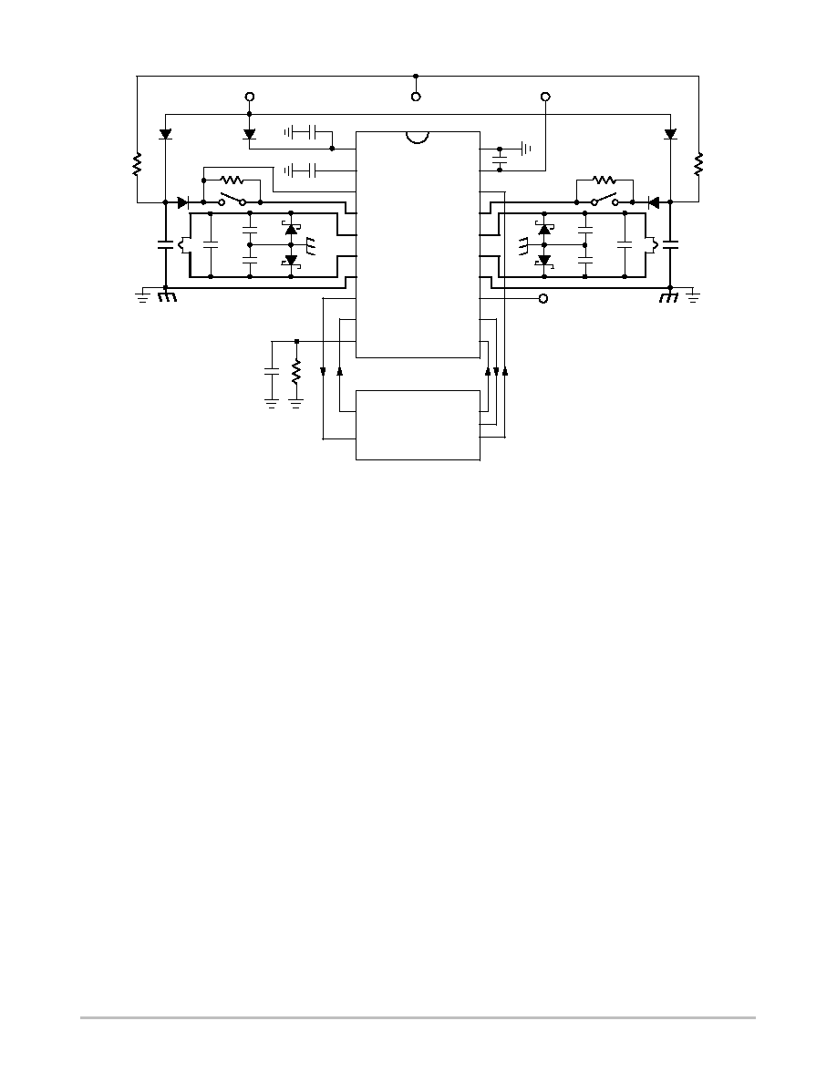
D
IN
VR2
SH2
SL2
FG2
A
IN
A
OUT
CS
V
BAT
CHRG
V
RES
VR1
SH1
SL1
FG1
D
OUT
CLK
MR
CS2082
C
CM
C
CM
C
CM
C
CM
C
DM
C
DM
+
+
C
RES
C
RES
MCU
C
MR
V
IGN
V
CC
V
BOOST
Analog
Input
Figure 3. Application Diagram
CS2082
http://onsemi.com
10
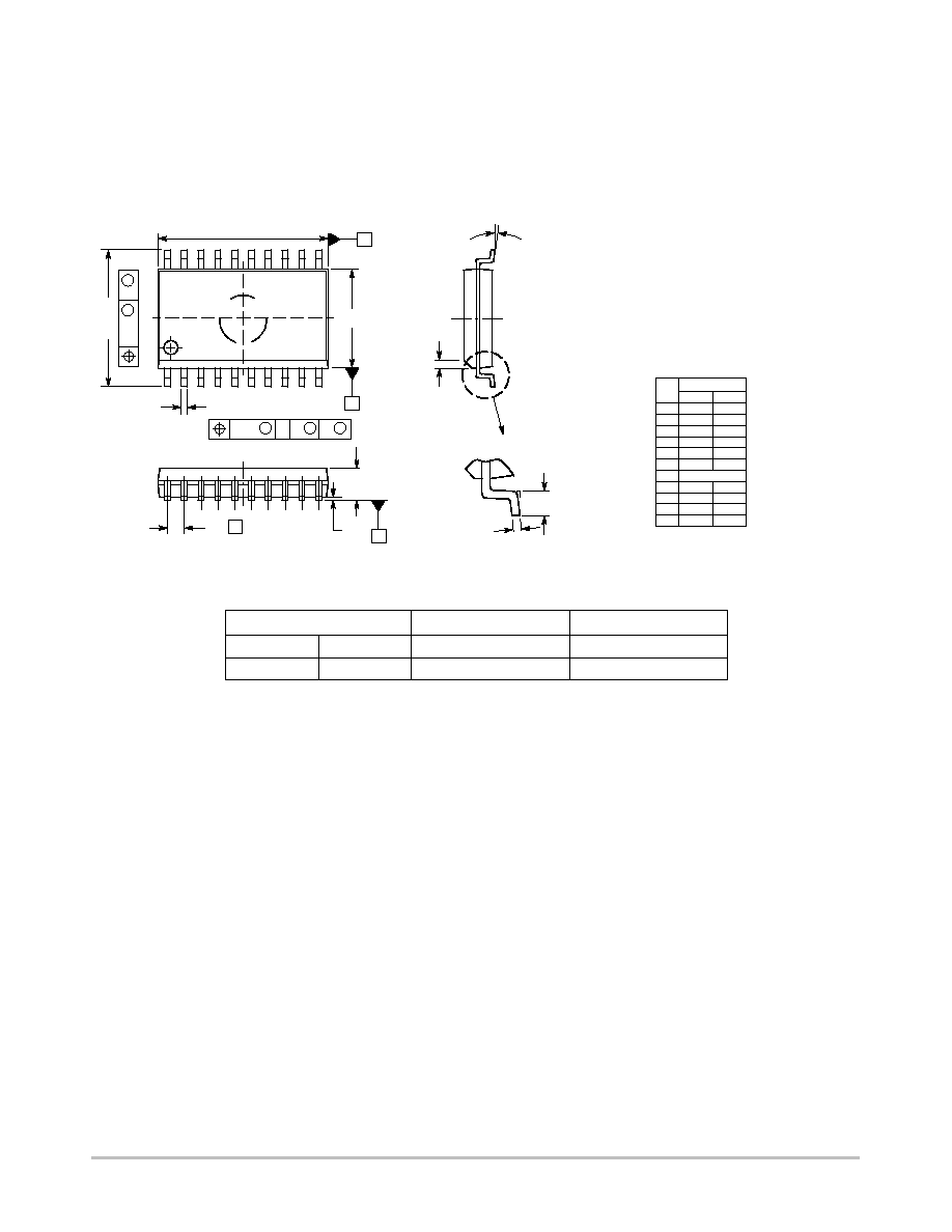
PACKAGE DIMENSIONS
SO≠20L
DW SUFFIX
CASE 751D≠05
ISSUE F
20
1
11
10
B
20X
H
10X
C
L
18X
A1
A
SEATING
PLANE
q
h
X 45
_
E
D
M
0.25
M
B
M
0.25
S
A
S
B
T
e
T
B
A
DIM
MIN
MAX
MILLIMETERS
A
2.35
2.65
A1
0.10
0.25
B
0.35
0.49
C
0.23
0.32
D
12.65
12.95
E
7.40
7.60
e
1.27 BSC
H
10.05
10.55
h
0.25
0.75
L
0.50
0.90
q
0
7
NOTES:
1. DIMENSIONS ARE IN MILLIMETERS.
2. INTERPRET DIMENSIONS AND TOLERANCES
PER ASME Y14.5M, 1994.
3. DIMENSIONS D AND E DO NOT INCLUDE MOLD
PROTRUSION.
4. MAXIMUM MOLD PROTRUSION 0.15 PER SIDE.
5. DIMENSION B DOES NOT INCLUDE DAMBAR
PROTRUSION. ALLOWABLE PROTRUSION SHALL
BE 0.13 TOTAL IN EXCESS OF B DIMENSION AT
MAXIMUM MATERIAL CONDITION.
_
_
PACKAGE THERMAL DATA
Parameter
SO≠20L
Unit
R
JC
Typical
17
∞
C/W
R
JA
Typical
90
∞
C/W

CS2082
http://onsemi.com
11
Notes

CS2082
http://onsemi.com
12
ON Semiconductor and are trademarks of Semiconductor Components Industries, LLC (SCILLC). SCILLC reserves the right to make changes
without further notice to any products herein. SCILLC makes no warranty, representation or guarantee regarding the suitability of its products for any particular
purpose, nor does SCILLC assume any liability arising out of the application or use of any product or circuit, and specifically disclaims any and all liability,
including without limitation special, consequential or incidental damages. "Typical" parameters which may be provided in SCILLC data sheets and/or
specifications can and do vary in different applications and actual performance may vary over time. All operating parameters, including "Typicals" must be
validated for each customer application by customer's technical experts. SCILLC does not convey any license under its patent rights nor the rights of others.
SCILLC products are not designed, intended, or authorized for use as components in systems intended for surgical implant into the body, or other applications
intended to support or sustain life, or for any other application in which the failure of the SCILLC product could create a situation where personal injury or
death may occur. Should Buyer purchase or use SCILLC products for any such unintended or unauthorized application, Buyer shall indemnify and hold
SCILLC and its officers, employees, subsidiaries, affiliates, and distributors harmless against all claims, costs, damages, and expenses, and reasonable
attorney fees arising out of, directly or indirectly, any claim of personal injury or death associated with such unintended or unauthorized use, even if such claim
alleges that SCILLC was negligent regarding the design or manufacture of the part. SCILLC is an Equal Opportunity/Affirmative Action Employer.
PUBLICATION ORDERING INFORMATION
JAPAN: ON Semiconductor, Japan Customer Focus Center
4≠32≠1 Nishi≠Gotanda, Shinagawa≠ku, Tokyo, Japan 141≠0031
Phone: 81≠3≠5740≠2700
Email: r14525@onsemi.com
ON Semiconductor Website: http://onsemi.com
For additional information, please contact your local
Sales Representative.
CS2082/D
Literature Fulfillment:
Literature Distribution Center for ON Semiconductor
P.O. Box 5163, Denver, Colorado 80217 USA
Phone: 303≠675≠2175 or 800≠344≠3860 Toll Free USA/Canada
Fax: 303≠675≠2176 or 800≠344≠3867 Toll Free USA/Canada
Email: ONlit@hibbertco.com
N. American Technical Support: 800≠282≠9855 Toll Free USA/Canada