 | –≠–Ľ–Ķ–ļ—ā—Ä–ĺ–Ĺ–Ĺ—č–Ļ –ļ–ĺ–ľ–Ņ–ĺ–Ĺ–Ķ–Ĺ—ā: LM293 | –°–ļ–į—á–į—ā—Ć:  PDF PDF  ZIP ZIP |
©
Semiconductor Components Industries, LLC, 2002
October, 2002 ≠ Rev. 10
1
Publication Order Number:
LM393/D
LM393, LM293, LM2903,
LM2903V, NCV2903
Low Offset Voltage
Dual Comparators
The LM393 series are dual independent precision voltage
comparators capable of single or split supply operation. These devices
are designed to permit a common mode range≠to≠ground level with
single supply operation. Input offset voltage specifications as low as
2.0 mV make this device an excellent selection for many applications
in consumer, automotive, and industrial electronics.
∑
Wide Single≠Supply Range: 2.0 Vdc to 36 Vdc
∑
Split≠Supply Range:
Ī
1.0 Vdc to
Ī
18 Vdc
∑
Very Low Current Drain Independent of Supply Voltage: 0.4 mA
∑
Low Input Bias Current: 25 nA
∑
Low Input Offset Current: 5.0 nA
∑
Low Input Offset Voltage: 5.0 mV (max) LM293/393
∑
Input Common Mode Range to Ground Level
∑
Differential Input Voltage Range Equal to Power Supply Voltage
∑
Output Voltage Compatible with DTL, ECL, TTL, MOS, and CMOS
Logic Levels
∑
ESD Clamps on the Inputs Increase the Ruggedness of the Device
without Affecting Performance
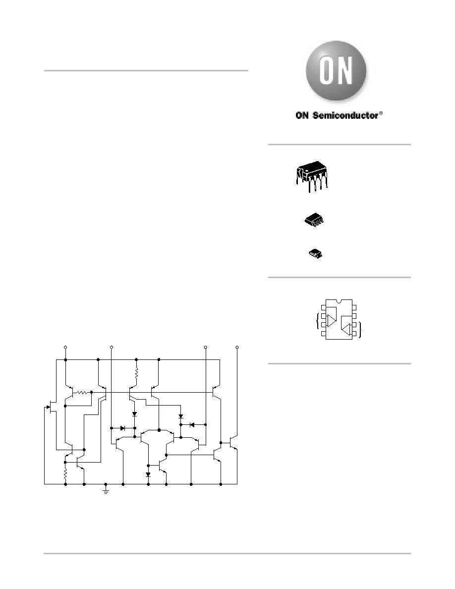
V
CC
+ Input
- Input
Output
Q3
R4
Q4
Q5
R2
Q6
Q14
Q16
Q15
Q12
Q11
Q10
Q9
Q8
Q2
Q1
F1
2.0 k
2.1 k
R1
4.6 k
Figure 1. Representative Schematic Diagram
(Diagram shown is for 1 comparator)
See detailed ordering and shipping information and marking
information in the package dimensions section on page 6 of
this data sheet.
ORDERING & DEVICE MARKING
INFORMATION
PDIP≠8
N SUFFIX
CASE 626
1
8
SO≠8
D SUFFIX
CASE 751
1
8
PIN CONNECTIONS
(Top View)
Gnd
Inputs A
Inputs B
Output B
Output A
V
CC
≠
≠
+
+
1
2
3
4
8
7
6
5
http://onsemi.com
Micro8
E
DM SUFFIX
CASE 846A
8
1
LM393, LM293, LM2903, LM2903V, NCV2903
http://onsemi.com
2
MAXIMUM RATINGS
Rating
Symbol
Value
Unit
Power Supply Voltage
V
CC
+36 or
Ī
18
Vdc
Input Differential Voltage Range
V
IDR
36
Vdc
Input Common Mode Voltage Range
V
ICR
≠0.3 to +36
Vdc
Output Short Circuit≠to≠Ground
I
SC
Continuous
mA
Output Sink Current (Note 1)
I
Sink
20
Power Dissipation @ T
A
= 25
į
C
P
D
570
mW
Derate above 25
į
C
1/R
q
JA
5.7
mW/
į
C
Operating Ambient Temperature Range
T
A
į
C
LM293
≠25 to +85
LM393
0 to +70
LM2903
≠40 to +105
LM2903V, NCV2903 (Note 2)
≠40 to +125
Maximum Operating Junction Temperature
T
J(max)
į
C
LM393, 2903, LM2903V
150
LM293, NCV2903
150
Storage Temperature Range
T
stg
≠65 to +150
į
C
1. The maximum output current may be as high as 20 mA, independent of the magnitude of V
CC
, output short circuits to V
CC
can cause
excessive heating and eventual destruction.
2.
NCV2903 is qualified for automotive use.
LM393, LM293, LM2903, LM2903V, NCV2903
http://onsemi.com
3
ELECTRICAL CHARACTERISTICS
(V
CC
= 5.0 Vdc, T
low
T
A
T
high
, unless otherwise noted.)
LM293, LM393
LM2903, LM2903V,
NCV2903
Characteristic
Symbol
Min
Typ
Max
Min
Typ
Max
Unit
Input Offset Voltage (Note 4)
V
IO
mV
T
A
= 25
į
C
≠
Ī
1.0
Ī
5.0
≠
Ī
2.0
Ī
7.0
T
low
T
A
T
high
≠
≠
9.0
≠
9.0
15
Input Offset Current
I
IO
nA
T
A
= 25
į
C
≠
Ī
5.0
Ī
50
≠
Ī
5.0
Ī
50
T
low
T
A
T
high
≠
≠
Ī
150
≠
Ī
50
Ī
200
Input Bias Current (Note 5)
I
IB
nA
T
A
= 25
į
C
≠
25
250
≠
25
250
T
low
T
A
T
high
≠
≠
400
≠
200
500
Input Common Mode Voltage Range (Note 5)
V
ICR
V
T
A
= 25
į
C
0
≠
V
CC
≠1.5
0
≠
V
CC
≠1.5
T
low
T
A
T
high
0
≠
V
CC
≠2.0
0
≠
V
CC
≠2.0
Voltage Gain
A
VOL
50
200
≠
25
200
≠
V/mV
R
L
15 k
W
, V
CC
= 15 Vdc, T
A
= 25
į
C
Large Signal Response Time
≠
≠
300
≠
≠
300
≠
ns
V
in
= TTL Logic Swing, V
ref
= 1.4 Vdc
V
RL
= 5.0 Vdc, R
L
= 5.1 k
W
, T
A
= 25
į
C
Response Time (Note 7)
t
TLH
≠
1.3
≠
≠
1.5
≠
m
s
V
RL
= 5.0 Vdc, R
L
= 5.1 k
W
, T
A
= 25
į
C
Input Differential Voltage (Note 8)
V
ID
≠
≠
V
CC
≠
≠
V
CC
V
All V
in
Gnd or V≠ Supply (if used)
Output Sink Current
I
Sink
6.0
16
≠
6.0
16
≠
mA
V
in
1.0 Vdc, V
in+
= 0 Vdc, V
O
1.5 Vdc T
A
= 25
į
C
Output Saturation Voltage
V
OL
mV
V
in
1.0 Vdc, V
in+
= 0, I
Sink
4.0 mA, T
A
= 25
į
C
≠
150
400
≠
≠
400
T
low
T
A
T
high
≠
≠
700
≠
200
700
Output Leakage Current
I
OL
nA
V
in≠
= 0 V, V
in+
1.0 Vdc, V
O
= 5.0 Vdc, T
A
= 25
į
C
≠
0.1
≠
≠
0.1
≠
V
in≠
= 0 V, V
in+
1.0 Vdc, V
O
= 30 Vdc,
T
low
T
A
T
high
≠
≠
1000
≠
≠
1000
Supply Current
I
CC
mA
R
L
=
Both Comparators, T
A
= 25
į
C
≠
0.4
1.0
≠
0.4
1.0
R
L
=
Both Comparators, V
CC
= 30 V
≠
≠
2.5
≠
≠
2.5
LM293 T
low
= ≠25
į
C, T
high
= +85
į
C
LM393 T
low
= 0
į
C, T
high
= +70
į
C
LM2903 T
low
= ≠40
į
C, T
high
= +105
į
C
LM2903V & NCV2903 T
low
= ≠40
į
C, T
high
= +125
į
C
NCV2903 is qualified for automotive use.
3. The maximum output current may be as high as 20 mA, independent of the magnitude of V
CC
, output short circuits to V
CC
can cause
excessive heating and eventual destruction.
4. At output switch point, V
O
]
1.4 Vdc, R
S
= 0
W
with V
CC
from 5.0 Vdc to 30 Vdc, and over the full input common mode range (0 V to
V
CC
= ≠1.5 V).
5. Due to the PNP transistor inputs, bias current will flow out of the inputs. This current is essentially constant, independent of the output state,
therefore, no loading changes will exist on the input lines.
6. Input common mode of either input should not be permitted to go more than 0.3 V negative of ground or minus supply. The upper limit of
common mode range is V
CC
≠1.5 V.
7. Response time is specified with a 100 mV step and 5.0 mV of overdrive. With larger magnitudes of overdrive faster response times are
obtainable.
8. The comparator will exhibit proper output state if one of the inputs becomes greater than V
CC
, the other input must remain within the common
mode range. The low input state must not be less than ≠0.3 V of ground or minus supply.
LM393, LM293, LM2903, LM2903V, NCV2903
http://onsemi.com
4
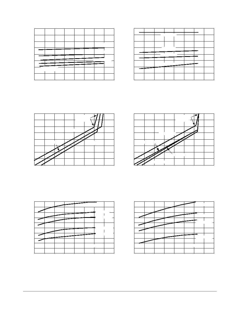
LM293/393
LM2903
Figure 2. Input Bias Current versus
Power Supply Voltage
Figure 3. Input Bias Current versus
Power Supply Voltage
Figure 4. Output Saturation Voltage
versus Output Sink Current
Figure 5. Output Saturation Voltage
versus Output Sink Current
Figure 6. Power Supply Current versus
Power Supply Voltage
Figure 7. Power Supply Current versus
Power Supply Voltage
V
CC
, SUPPLY VOLTAGE (Vdc)
V
CC
, SUPPLY VOLTAGE (Vdc)
V
CC
, SUPPLY VOLTAGE (Vdc)
V
CC
, SUPPLY VOLTAGE (Vdc)
I
Sink
, OUTPUT SINK CURRENT (mA)
I
Sink
, OUTPUT SINK CURRENT (mA)
I , INPUT
BIAS CURRENT
(nA)
IB
V , SA
TURA
TION VOL
T
AGE (Vdc)
OL
I , SUPPL
Y
CURRENT
(mA)
CC
80
70
60
50
40
30
20
10
0
0
5.0
10
15
20
25
30
35
40
80
70
60
50
40
30
20
10
0
0
5.0
10
15
20
25
30
35
40
10
1.0
0.1
0.01
0.001
0.01
0.1
1.0
10
100
1.0
0.8
0.6
0.4
0.2
0
5.0
10
15
20
25
30
35
40
1.2
0.4
10
1.0
0.1
0.01
0.001
0.01
0.1
1.0
10
100
0
5.0
10
15
20
25
30
35
40
T
A
= 0
į
C
T
A
= +25
į
C
T
A
= +25
į
C
T
A
= +85
į
C
T
A
= -40
į
C
T
A
= +70
į
C
T
A
= +125
į
C
R
L
=
R
T
A
= 0
į
C
T
A
= +25
į
C
T
A
= +25
į
C
T
A
= 0
į
C
T
A
= +25
į
C
T
A
= -40
į
C
T
A
= -40
į
C
T
A
= 0
į
C
T
A
= +25
į
C
T
A
= +85
į
C
1.0
0.8
0.6
I , SUPPL
Y
CURRENT
(mA)
CC
V , SA
TURA
TION VOL
T
AGE (Vdc)
OL
I , INPUT
BIAS CURRENT
(nA)
IB
T
A
= +125
į
C
R
L
=
R
T
A
= -55
į
C
T
A
= +70
į
C
T
A
= +125
į
C
T
A
= -55
į
C
Out of
Saturation
T
A
= +85
į
C
Out of
Saturation
T
A
= -55
į
C
T
A
= 0
į
C
LM393, LM293, LM2903, LM2903V, NCV2903
http://onsemi.com
5
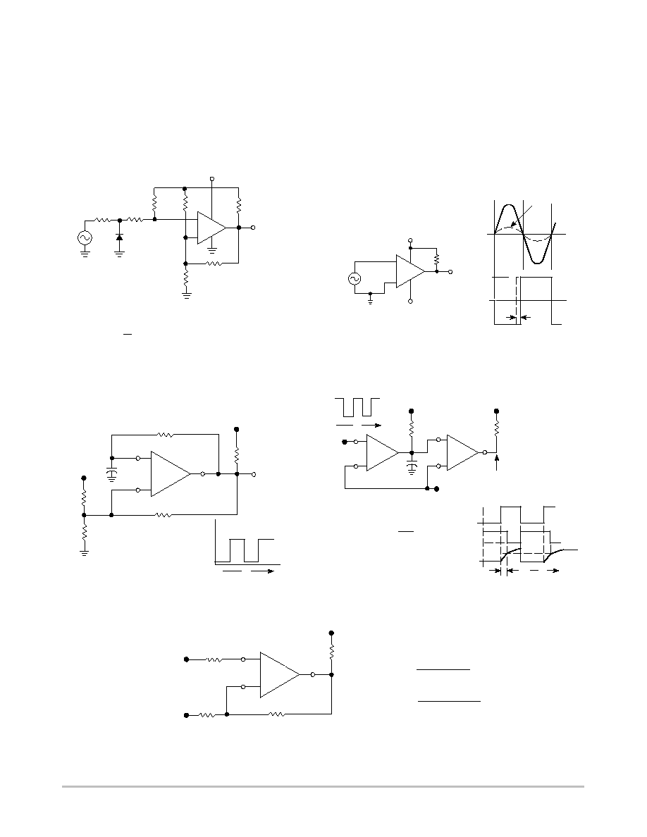
APPLICATIONS INFORMATION
These dual comparators feature high gain, wide
bandwidth characteristics. This gives the device oscillation
tendencies if the outputs are capacitively coupled to the
inputs via stray capacitance. This oscillation manifests itself
during output transitions (V
OL
to V
OH
). To alleviate this
situation, input resistors <10 k
W should be used.
The addition of positive feedback (<10 mV) is also
recommended. It is good design practice to ground all
unused pins.
Differential input voltages may be larger than supply
voltage without damaging the comparator's inputs. Voltages
more negative than ≠0.3 V should not be used.
Figure 8. Zero Crossing Detector
(Single Supply)
Figure 9. Zero Crossing Detector
(Split Supply)
Figure 10. Free≠Running Square≠Wave Oscillator
Figure 11. Time Delay Generator
Figure 12. Comparator with Hysteresis
10
D1 prevents input from going negative by more than 0.6 V.
R1 + R2 = R3
R3
R5
for small error in zero crossing.
V
in
10 k
D1
R1
8.2 k
6.8 k
R2
15 k
R3
+15 V
10 M
R5
220 k
R4
220 k
LM393
V
in(min)
[ 0.4 V peak for 1% phase distortion (DQ).
*
Q
+V
CC
10 k
V
in
-V
EE
V
in
V
in(min)
V
CC
V
O
- V
EE
DQ
Q
LM393
-
+
LM393
51 k
51 k
51 k
R
L
10 k
V
CC
V
CC
V
CC
V
O
V
O
t
0
1.0 MW
0.001 mF
-
+
LM393
V
CC
V
CC
V
O
V
in
V
O
+ V
ref
V
ref
V
ref
0
0
0
V
C
t
O
t
``ON'' for t t
O
+ Dt
where:
Dt = RC n (
V
ref
V
CC
)
R
R
L
V
C
C
LM393
-
+
R
S
V
CC
R
L
V
ref
R1
R2
R
S
= R1 | | R2
V
th1
= V
ref
+
(V
CC
-V
ref
) R1
R1 + R2 + R
L
V
th2
= V
ref
-
(V
ref
-V
O
Low) R1
R1 + R2
R1
t
-
+
LM393
)
*
)

LM393, LM293, LM2903, LM2903V, NCV2903
http://onsemi.com
6
MARKING DIAGRAMS
AWL
LM393N
1
8
YYWW
x
= 2 or 3
A
= Assembly Location
WL, L
= Wafer Lot
YY, Y
= Year
WW, W = Work Week
ALYW
LMx93
1
8
PDIP≠8
N SUFFIX
CASE 626
AWL
LM2903N
1
8
YYWW
SO≠8
D SUFFIX
CASE 751
ALYW
2903
1
8
ALYW
2903V
1
8
*
*This marking diagram also applies to NCV2903DR2.
Micro8
DM SUFFIX
CASE 846A
x93
AYW
1
8
2903
AYW
1
8
ORDERING INFORMATION
Device
Package
Shipping
LM293D
SO≠8
98 Units / Rail
LM293DR2
SO≠8
2500 Units / Reel
LM293DMR2
Micro8
4000 Tape and Reel
LM393D
SO≠8
98 Units / Rail
LM393DR2
SO≠8
2500 Units / Reel
LM393N
PDIP8
50 Units / Rail
LM393DMR2
Micro8
4000 Tape and Reel
LM2903D
SO≠8
98 Units / Reel
LM2903DR2
SO≠8
2500 Units /Reel
LM2903N
PDIP8
50 Units / Rail
LM2903DMR2
Micro8
4000 Tape and Reel
LM2903VD
SO≠8
98 Units / Reel
LM2903VDR2
SO≠8
2500 Units /Reel
LM2903VN
PDIP8
50 Units / Rail
NCV2903DR2 (Note 9)
SO≠8
2500 Tape and Reel
NCV2903DMR2 (Note 9)
Micro8
4000 Tape and Reel
9. NCV2903 is qualified for automotive use.

LM393, LM293, LM2903, LM2903V, NCV2903
http://onsemi.com
7
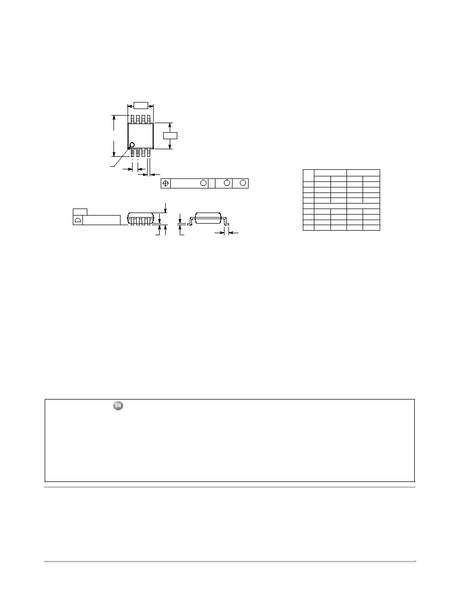
PACKAGE DIMENSIONS
PDIP≠8
N SUFFIX
CASE 626≠05
ISSUE L
NOTES:
1. DIMENSION L TO CENTER OF LEAD WHEN
FORMED PARALLEL.
2. PACKAGE CONTOUR OPTIONAL (ROUND OR
SQUARE CORNERS).
3. DIMENSIONING AND TOLERANCING PER ANSI
Y14.5M, 1982.
1
4
5
8
F
NOTE 2
≠A≠
≠B≠
≠T≠
SEATING
PLANE
H
J
G
D
K
N
C
L
M
M
A
M
0.13 (0.005)
B
M
T
DIM
MIN
MAX
MIN
MAX
INCHES
MILLIMETERS
A
9.40
10.16
0.370
0.400
B
6.10
6.60
0.240
0.260
C
3.94
4.45
0.155
0.175
D
0.38
0.51
0.015
0.020
F
1.02
1.78
0.040
0.070
G
2.54 BSC
0.100 BSC
H
0.76
1.27
0.030
0.050
J
0.20
0.30
0.008
0.012
K
2.92
3.43
0.115
0.135
L
7.62 BSC
0.300 BSC
M
---
10
---
10
N
0.76
1.01
0.030
0.040
_
_
SO≠8
D SUFFIX
CASE 751≠07
ISSUE AA
SEATING
PLANE
1
4
5
8
N
J
X 45
_
K
NOTES:
1. DIMENSIONING AND TOLERANCING PER ANSI
Y14.5M, 1982.
2. CONTROLLING DIMENSION: MILLIMETER.
3. DIMENSION A AND B DO NOT INCLUDE MOLD
PROTRUSION.
4. MAXIMUM MOLD PROTRUSION 0.15 (0.006) PER
SIDE.
5. DIMENSION D DOES NOT INCLUDE DAMBAR
PROTRUSION. ALLOWABLE DAMBAR
PROTRUSION SHALL BE 0.127 (0.005) TOTAL IN
EXCESS OF THE D DIMENSION AT MAXIMUM
MATERIAL CONDITION.
6. 751-01 THRU 751-06 ARE OBSOLETE. NEW
STANDAARD IS 751-07
A
B
S
D
H
C
0.10 (0.004)
DIM
A
MIN
MAX
MIN
MAX
INCHES
4.80
5.00
0.189
0.197
MILLIMETERS
B
3.80
4.00
0.150
0.157
C
1.35
1.75
0.053
0.069
D
0.33
0.51
0.013
0.020
G
1.27 BSC
0.050 BSC
H
0.10
0.25
0.004
0.010
J
0.19
0.25
0.007
0.010
K
0.40
1.27
0.016
0.050
M
0
8
0
8
N
0.25
0.50
0.010
0.020
S
5.80
6.20
0.228
0.244
≠X≠
≠Y≠
G
M
Y
M
0.25 (0.010)
≠Z≠
Y
M
0.25 (0.010)
Z
S
X
S
M
_
_
_
_
LM393, LM293, LM2903, LM2903V, NCV2903
http://onsemi.com
8
PACKAGE DIMENSIONS
S
B
M
0.08 (0.003)
A
S
T
DIM
MIN
MAX
MIN
MAX
INCHES
MILLIMETERS
A
2.90
3.10
0.114
0.122
B
2.90
3.10
0.114
0.122
C
---
1.10
---
0.043
D
0.25
0.40
0.010
0.016
G
0.65 BSC
0.026 BSC
H
0.05
0.15
0.002
0.006
J
0.13
0.23
0.005
0.009
K
4.75
5.05
0.187
0.199
L
0.40
0.70
0.016
0.028
NOTES:
1. DIMENSIONING AND TOLERANCING PER ANSI
Y14.5M, 1982.
2. CONTROLLING DIMENSION: MILLIMETER.
3. DIMENSION A DOES NOT INCLUDE MOLD FLASH,
PROTRUSIONS OR GATE BURRS. MOLD FLASH,
PROTRUSIONS OR GATE BURRS SHALL NOT
EXCEED 0.15 (0.006) PER SIDE.
4. DIMENSION B DOES NOT INCLUDE INTERLEAD
FLASH OR PROTRUSION. INTERLEAD FLASH OR
PROTRUSION SHALL NOT EXCEED 0.25 (0.010)
PER SIDE.
5. 846A-01 OBSOLETE, NEW STANDARD 846A-02.
≠B≠
≠A≠
D
K
G
PIN 1 ID
8 PL
0.038 (0.0015)
≠T≠
SEATING
PLANE
C
H
J
L
Micro8
DM SUFFIX
CASE 846A≠02
ISSUE F
ON Semiconductor and are registered trademarks of Semiconductor Components Industries, LLC (SCILLC). SCILLC reserves the right to make
changes without further notice to any products herein. SCILLC makes no warranty, representation or guarantee regarding the suitability of its products for any
particular purpose, nor does SCILLC assume any liability arising out of the application or use of any product or circuit, and specifically disclaims any and all
liability, including without limitation special, consequential or incidental damages. "Typical" parameters which may be provided in SCILLC data sheets and/or
specifications can and do vary in different applications and actual performance may vary over time. All operating parameters, including "Typicals" must be
validated for each customer application by customer's technical experts. SCILLC does not convey any license under its patent rights nor the rights of others.
SCILLC products are not designed, intended, or authorized for use as components in systems intended for surgical implant into the body, or other applications
intended to support or sustain life, or for any other application in which the failure of the SCILLC product could create a situation where personal injury or death
may occur. Should Buyer purchase or use SCILLC products for any such unintended or unauthorized application, Buyer shall indemnify and hold SCILLC
and its officers, employees, subsidiaries, affiliates, and distributors harmless against all claims, costs, damages, and expenses, and reasonable attorney fees
arising out of, directly or indirectly, any claim of personal injury or death associated with such unintended or unauthorized use, even if such claim alleges that
SCILLC was negligent regarding the design or manufacture of the part. SCILLC is an Equal Opportunity/Affirmative Action Employer.
PUBLICATION ORDERING INFORMATION
JAPAN: ON Semiconductor, Japan Customer Focus Center
2≠9≠1 Kamimeguro, Meguro≠ku, Tokyo, Japan 153≠0051
Phone: 81≠3≠5773≠3850
Email: r14525@onsemi.com
ON Semiconductor Website: http://onsemi.com
For additional information, please contact your local
Sales Representative.
LM393/D
Micro8 is a trademark of International Rectifier.
Literature Fulfillment:
Literature Distribution Center for ON Semiconductor
P.O. Box 5163, Denver, Colorado 80217 USA
Phone: 303≠675≠2175 or 800≠344≠3860 Toll Free USA/Canada
Fax: 303≠675≠2176 or 800≠344≠3867 Toll Free USA/Canada
Email: ONlit@hibbertco.com
N. American Technical Support: 800≠282≠9855 Toll Free USA/Canada