 | –≠–ª–µ–∫—Ç—Ä–æ–Ω–Ω—ã–π –∫–æ–º–ø–æ–Ω–µ–Ω—Ç: MC10H350 | –°–∫–∞—á–∞—Ç—å:  PDF PDF  ZIP ZIP |

MOTOROLA
SEMICONDUCTOR TECHNICAL DATA
2≠57
REV 6
©
Motorola, Inc. 1996
9/96
PECL* to TTL Translator
(+5 Vdc Power Supply Only)
The MC10H350 is a member of Motorola's 10H family of high performance
ECL logic. It consists of 4 translators with differential inputs and TTL outputs.
The 3≠state outputs can be disabled by applying a HIGH TTL logic level on the
common OE input.
The MC10H350 is designed to be used primarily in systems incorporating
both ECL and TTL logic operating off a common power supply. The separate
VCC power pins are not connected internally and thus isolate the noisy TTL VCC
runs from the relatively quiet ECL VCC runs on the printed circuit board. The
differential inputs allow the H350 to be used as an inverting or noninverting
translator, or a differential line receiver. The H350 can also drive CMOS with the
addition of a pullup resistor.
∑
Propagation Delay, 3.5 ns Typical
∑
MECL 10K≠Compatible
MAXIMUM RATINGS
Characteristic
Symbol
Rating
Unit
Power Supply (VEE = Gnd)
VCC
7.0
Vdc
Operating Temperature Range
TA
0 to +75
∞
C
Storage Temperature Range -- Plastic
-- Ceramic
Tstg
≠55 to +150
≠55 to +165
∞
C
∞
C
ELECTRICAL CHARACTERISTICS (VCC = 5.0 V
±
5%) (See Note 1)
TA = 0
∞
C to 75
∞
C
Characteristic
Symbol
Min
Max
Unit
Power Supply Current
TTL
ECL
ICC
--
--
20
12
mA
Input Current High
Pin 9
Others
IIH
IINH
--
--
20
50
µ
A
Input Current Low
Pin 9
Others
IIL
IINL
--
--
≠0.6
50
mA
µ
A
Input Voltage High
Pin 9
VIH
2.0
--
Vdc
Input Voltage Low
Pin 9
VIL
--
0.8
Vdc
Differential Input Voltage (1)
Pins 3≠6, 11≠14 (1)
VDIFF
350
--
mV
Voltage Common Mode
Pins 3≠6, 11≠14
VCM
2.8
VCC
Vdc
Output Voltage High
IOH = 3.0 mA
VOH
2.7
--
Vdc
Output Voltage Low
IOL = 20 mA
VOL
--
0.5
Vdc
Short Circuit Current
VOUT = 0 V
IOS
≠60
≠150
mA
Output Disable Current High
VOUT = 2.7 V
IOZH
--
50
µ
A
Output Disable Current Low
VOUT = 0.5 V
IOZL
--
≠50
µ
A
(1) Common mode input voltage to pins 3≠4, 5≠6, 11≠12, 13≠14 must be between the values of 2.8
V and 5.0 V. This common mode input voltage range includes the differential input swing.
(2) For single ended use, apply 3.75 V (VBB) to either input depending on output polarity required.
Signal level range to other input is 3.3 V to 4.2 V.
(3) Any unused gates should have the inverting inputs tied to VCC and the non≠inverting inputs tied
to ground to prevent output glitching.
(4) 1.0 V to 2.0 V w/50 pF into 500 ohms.
*Positive Emitter Coupled Logic
LOGIC DIAGRAM
DIP
PIN ASSIGNMENT
ECL VCC
AOUT
AIN
AIN
BIN
BIN
BOUT
GND
TTL VCC
COUT
CIN
CIN
DIN
DIN
DOUT
OE
16
15
14
13
12
11
10
9
1
2
3
4
5
6
7
8
VCC (+5.0 VDC) = PINS 1 AND 16
GND = PIN 8
15
14
13
10
12
11
7
6
5
2
4
3
9
MC10H350
L SUFFIX
CERAMIC PACKAGE
CASE 620≠10
P SUFFIX
PLASTIC PACKAGE
CASE 648≠08
FN SUFFIX
PLCC
CASE 775≠02
Pin assignment is for Dual≠in≠Line Package.
For PLCC pin assignment, see the Pin Conversion
Tables on page 6≠11 of the Motorola MECL Data
Book (DL122/D).
MC10H350
MOTOROLA
MECL Data
DL122 -- Rev 6
2≠58
ELECTRICAL CHARACTERISTICS (VCC = 5.0 V
±
5%) (See Notes 1 & 4)
TA = 0
∞
C to 75
∞
C
Characteristic
Symbol
Min
Max
Unit
AC PARAMETERS (CL = 50 pF) (VCC = 5.0
±
5%) (TA = 0
∞
C to 75
∞
C)
Propagation Delay
Data
tpd
1.5
5.0
ns
Rise Time
tr
0.3
1.6
ns
Fall Time
tf
0.3
1.6
ns
Output Disable Time
tpdLZ
tpdHZ
2.0
2.0
6.0
6.0
ns
Output Enable Time
tpdZL
tpdZH
2.0
2.0
8.0
8.0
ns
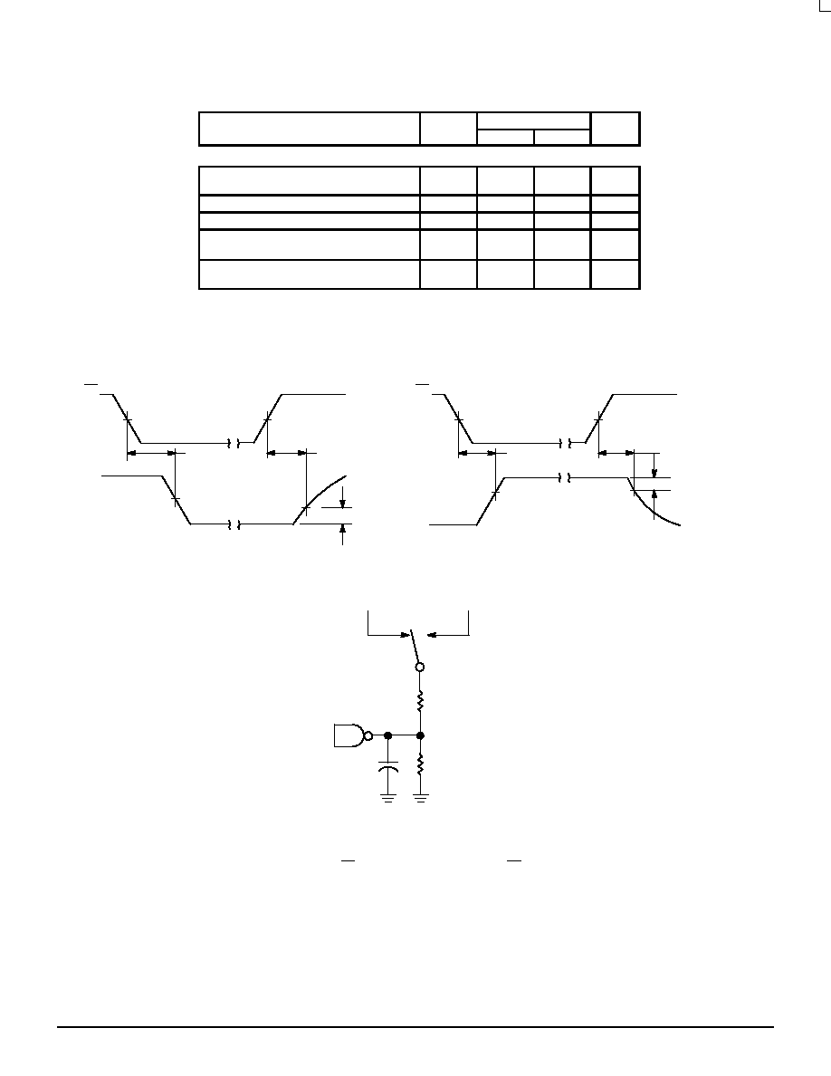
TPZL
0.3 V
OE
1.5 V
1.5 V
1.5 V
TPZH
TPHZ
3≠STATE OUTPUT HIGH ENABLE AND
DISABLE TIMES
OE
VOUT
0.3 V
VOL
1.5 V
1.5 V
1.5 V
TPLZ
Q
VOH
3.5 V
+7.0 V
OPEN
ALL OTHER
TPZL, TPLZ, O, C,
500
500
D.U.T
.
50 PF
3≠STATE SWITCHING WAVEFORMS
3≠STATE OUTPUT LOW ENABLE AND
DISABLE TIMES
TEST LOAD
*INCLUDES JIG AND PROBE CAPACITANCE
VOUT
Application Note: Pin 9 is an OE and the 10H350 is disabled when OE is at VIH or higher.
MC10H350
2≠59
MOTOROLA
MECL Data
DL122 -- Rev 6
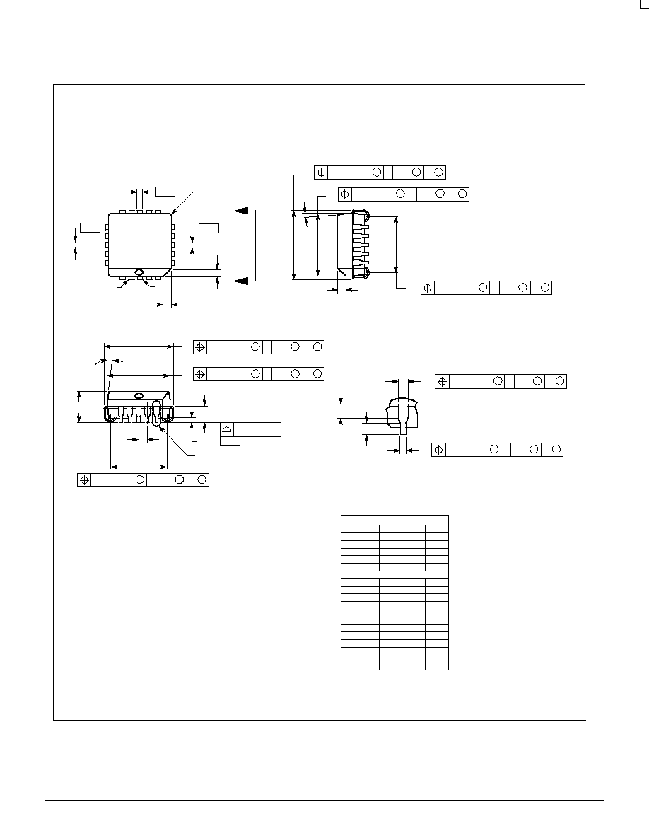
OUTLINE DIMENSIONS
FN SUFFIX
PLASTIC PLCC PACKAGE
CASE 775≠02
ISSUE C
NOTES:
1. DATUMS ≠L≠, ≠M≠, AND ≠N≠ DETERMINED
WHERE TOP OF LEAD SHOULDER EXITS PLASTIC
BODY AT MOLD PARTING LINE.
2. DIMENSION G1, TRUE POSITION TO BE
MEASURED AT DATUM ≠T≠, SEATING PLANE.
3. DIMENSIONS R AND U DO NOT INCLUDE MOLD
FLASH. ALLOWABLE MOLD FLASH IS 0.010 (0.250)
PER SIDE.
4. DIMENSIONING AND TOLERANCING PER ANSI
Y14.5M, 1982.
5. CONTROLLING DIMENSION: INCH.
6. THE PACKAGE TOP MAY BE SMALLER THAN THE
PACKAGE BOTTOM BY UP TO 0.012 (0.300).
DIMENSIONS R AND U ARE DETERMINED AT THE
OUTERMOST EXTREMES OF THE PLASTIC BODY
EXCLUSIVE OF MOLD FLASH, TIE BAR BURRS,
GATE BURRS AND INTERLEAD FLASH, BUT
INCLUDING ANY MISMATCH BETWEEN THE TOP
AND BOTTOM OF THE PLASTIC BODY.
7. DIMENSION H DOES NOT INCLUDE DAMBAR
PROTRUSION OR INTRUSION. THE DAMBAR
PROTRUSION(S) SHALL NOT CAUSE THE H
DIMENSION TO BE GREATER THAN 0.037 (0.940).
THE DAMBAR INTRUSION(S) SHALL NOT CAUSE
THE H DIMENSION TO BE SMALLER THAN 0.025
(0.635).
≠M≠
≠N≠
≠L≠
Y BRK
W
V
D
D
S
L≠M
M
0.007 (0.180)
N
S
T
S
L≠M
M
0.007 (0.180)
N
S
T
S
L≠M
S
0.010 (0.250)
N
S
T
X
G1
B
U
Z
VIEW D≠D
20
1
S
L≠M
M
0.007 (0.180)
N
S
T
S
L≠M
M
0.007 (0.180)
N
S
T
S
L≠M
S
0.010 (0.250)
N
S
T
C
G
VIEW S
E
J
R
Z
A
0.004 (0.100)
≠T≠
SEATING
PLANE
S
L≠M
M
0.007 (0.180)
N
S
T
S
L≠M
M
0.007 (0.180)
N
S
T
H
VIEW S
K
K1
F
G1
DIM
MIN
MAX
MIN
MAX
MILLIMETERS
INCHES
A
0.385
0.395
9.78
10.03
B
0.385
0.395
9.78
10.03
C
0.165
0.180
4.20
4.57
E
0.090
0.110
2.29
2.79
F
0.013
0.019
0.33
0.48
G
0.050 BSC
1.27 BSC
H
0.026
0.032
0.66
0.81
J
0.020
≠≠≠
0.51
≠≠≠
K
0.025
≠≠≠
0.64
≠≠≠
R
0.350
0.356
8.89
9.04
U
0.350
0.356
8.89
9.04
V
0.042
0.048
1.07
1.21
W
0.042
0.048
1.07
1.21
X
0.042
0.056
1.07
1.42
Y
≠≠≠
0.020
≠≠≠
0.50
Z
2
10
2
10
G1
0.310
0.330
7.88
8.38
K1
0.040
≠≠≠
1.02
≠≠≠
_
_
_
_
MC10H350
MOTOROLA
MECL Data
DL122 -- Rev 6
2≠60
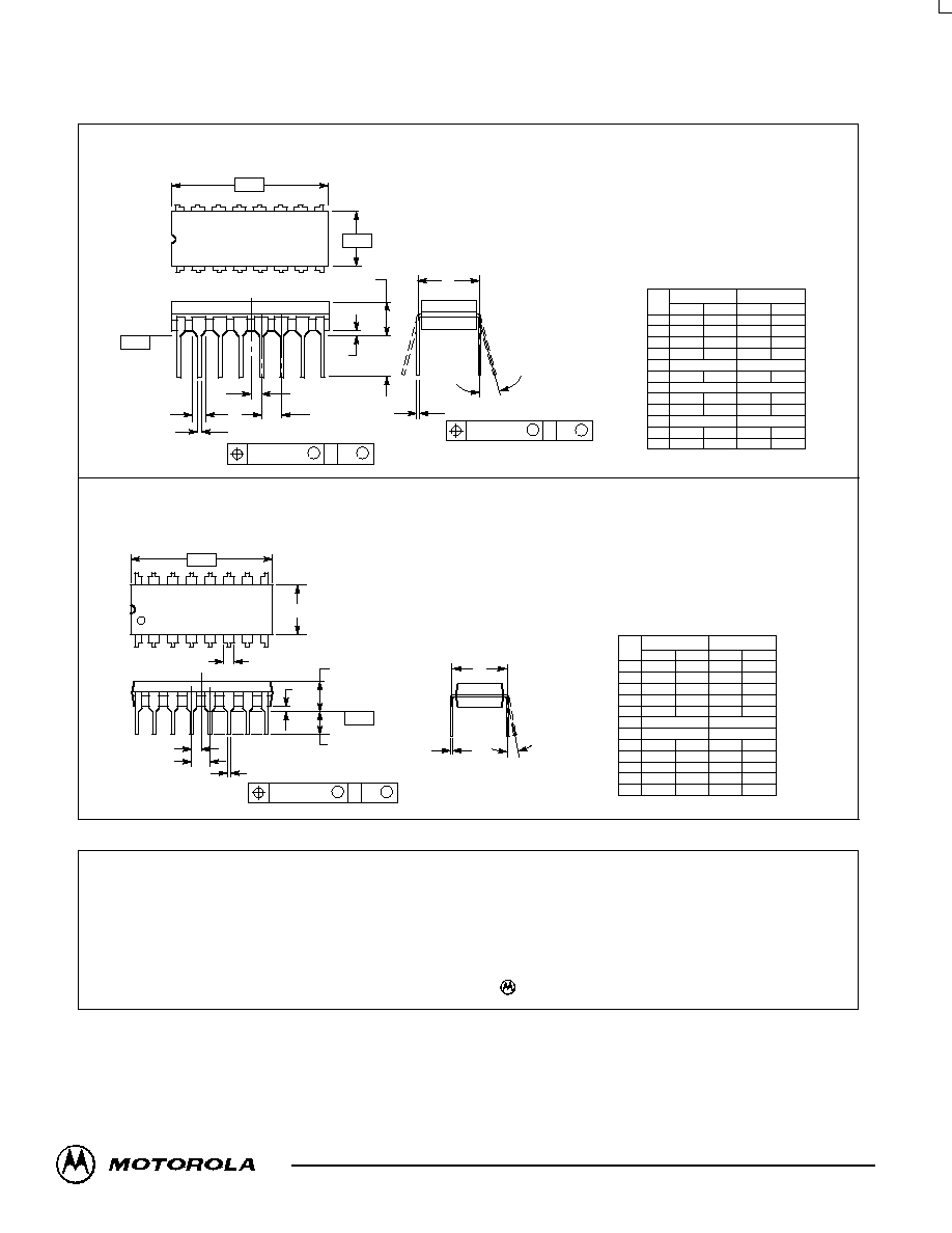
OUTLINE DIMENSIONS
P SUFFIX
PLASTIC DIP PACKAGE
CASE 648≠08
ISSUE R
NOTES:
1. DIMENSIONING AND TOLERANCING PER ANSI
Y14.5M, 1982.
2. CONTROLLING DIMENSION: INCH.
3. DIMENSION L TO CENTER OF LEADS WHEN
FORMED PARALLEL.
4. DIMENSION B DOES NOT INCLUDE MOLD FLASH.
5. ROUNDED CORNERS OPTIONAL.
≠A≠
B
F
C
S
H
G
D
J
L
M
16 PL
SEATING
1
8
9
16
K
PLANE
≠T≠
M
A
M
0.25 (0.010)
T
DIM
MIN
MAX
MIN
MAX
MILLIMETERS
INCHES
A
0.740
0.770
18.80
19.55
B
0.250
0.270
6.35
6.85
C
0.145
0.175
3.69
4.44
D
0.015
0.021
0.39
0.53
F
0.040
0.70
1.02
1.77
G
0.100 BSC
2.54 BSC
H
0.050 BSC
1.27 BSC
J
0.008
0.015
0.21
0.38
K
0.110
0.130
2.80
3.30
L
0.295
0.305
7.50
7.74
M
0
10
0
10
S
0.020
0.040
0.51
1.01
_
_
_
_
L SUFFIX
CERAMIC DIP PACKAGE
CASE 620≠10
ISSUE V
NOTES:
1. DIMENSIONING AND TOLERANCING PER
ANSI Y14.5M, 1982.
2. CONTROLLING DIMENSION: INCH.
3. DIMENSION L TO CENTER OF LEAD WHEN
FORMED PARALLEL.
4. DIMENSION F MAY NARROW TO 0.76 (0.030)
WHERE THE LEAD ENTERS THE CERAMIC
BODY.
≠A≠
≠B≠
≠T≠
F
E
G
N
K
C
SEATING
PLANE
16 PL
D
S
A
M
0.25 (0.010)
T
16 PL
J
S
B
M
0.25 (0.010)
T
M
L
DIM
MIN
MAX
MIN
MAX
MILLIMETERS
INCHES
A
0.750
0.785
19.05
19.93
B
0.240
0.295
6.10
7.49
C
≠≠≠
0.200
≠≠≠
5.08
D
0.015
0.020
0.39
0.50
E
0.050 BSC
1.27 BSC
F
0.055
0.065
1.40
1.65
G
0.100 BSC
2.54 BSC
H
0.008
0.015
0.21
0.38
K
0.125
0.170
3.18
4.31
L
0.300 BSC
7.62 BSC
M
0
15
0
15
N
0.020
0.040
0.51
1.01
_
_
_
_
16
9
1
8
Motorola reserves the right to make changes without further notice to any products herein. Motorola makes no warranty, representation or guarantee regarding
the suitability of its products for any particular purpose, nor does Motorola assume any liability arising out of the application or use of any product or circuit, and
specifically disclaims any and all liability, including without limitation consequential or incidental damages. "Typical" parameters which may be provided in Motorola
data sheets and/or specifications can and do vary in different applications and actual performance may vary over time. All operating parameters, including "Typicals"
must be validated for each customer application by customer's technical experts. Motorola does not convey any license under its patent rights nor the rights of
others. Motorola products are not designed, intended, or authorized for use as components in systems intended for surgical implant into the body, or other
applications intended to support or sustain life, or for any other application in which the failure of the Motorola product could create a situation where personal injury
or death may occur. Should Buyer purchase or use Motorola products for any such unintended or unauthorized application, Buyer shall indemnify and hold Motorola
and its officers, employees, subsidiaries, affiliates, and distributors harmless against all claims, costs, damages, and expenses, and reasonable attorney fees
arising out of, directly or indirectly, any claim of personal injury or death associated with such unintended or unauthorized use, even if such claim alleges that
Motorola was negligent regarding the design or manufacture of the part. Motorola and are registered trademarks of Motorola, Inc. Motorola, Inc. is an Equal
Opportunity/Affirmative Action Employer.
How to reach us:
USA/EUROPE/Locations Not Listed: Motorola Literature Distribution;
JAPAN: Nippon Motorola Ltd.; Tatsumi≠SPD≠JLDC, 6F Seibu≠Butsuryu≠Center,
P.O. Box 20912; Phoenix, Arizona 85036. 1≠800≠441≠2447 or 602≠303≠5454
3≠14≠2 Tatsumi Koto≠Ku, Tokyo 135, Japan. 03≠81≠3521≠8315
MFAX: RMFAX0@email.sps.mot.com ≠ TOUCHTONE 602≠244≠6609
ASIA/PACIFIC: Motorola Semiconductors H.K. Ltd.; 8B Tai Ping Industrial Park,
INTERNET: http://Design≠NET.com
51 Ting Kok Road, Tai Po, N.T., Hong Kong. 852≠26629298
MC10H350/D
*MC10H350/D*