©
Semiconductor Components Industries, LLC, 2001
November, 2001 ≠ Rev. 7
1
Publication Order Number:
MC12026A/D
MC12026A
1.1 GHz Dual Modulus
Prescaler
The MC12026 is a high frequency, low voltage dual modulus
prescaler used in phase≠locked loop (PLL) applications.
The MC12026A can be used with CMOS synthesizers requiring
positive edges to trigger internal counters in a PLL to provide tuning
signals up to 1.1 GHz in programmable frequency steps.
A Divide Ratio Control (SW) permits selection of an 8/9 or 16/17
divide ratio as desired.
The Modulus Control (MC) selects the proper divide number after
SW has been biased to select the desired divide ratio.
Features
∑
1.1 GHz Toggle Frequency
∑
Supply Voltage 4.5 to 5.5 V
∑
Low Power 4.0 mA Typical
∑
Operating Temperature Range of ≠40 to 85
∞
C
∑
The MC12026 is Pin Compatible with the MC12022
∑
Short Setup Time (tset ) 6.0 ns Typical @ 1.1 GHz
∑
Modulus Control Input Level is Compatible with Standard CMOS
and TTL
FUNCTIONAL TABLE
SW
MC
Divide Ratio
H
H
8
H
L
9
L
H
16
L
L
17
1. SW: H = VCC, L = Open. A logic L can also be applied by grounding this pin,
but this is not recommended due to increased power consumption.
2. MC: H = 2.0 V to VCC, L = GND to 0.8 V.
MAXIMUM RATINGS
Characteristics
Symbol
Value
Unit
Power Supply Voltage, Pin 2
VCC
≠0.5 to 7.0
Vdc
Operating Temperature Range
TA
≠40 to 85
∞
C
Storage Temperature Range
Tstg
≠65 to 150
∞
C
Modulus Control Input, Pin 6
MC
≠0.5 to 6.5
Vdc
Maximum Output Current, Pin 4
IO
10.0
mA
NOTE: ESD data available upon request.
http://onsemi.com
SO≠8
D SUFFIX
CASE 751
8
1
PIN CONNECTIONS
Device
Package
Shipping
ORDERING INFORMATION
MC12026AD
SO≠8
98 Units/Rail
MC12026ADR2
SO≠8
2500 Tape & Reel
(Top View)
IN
8
IN
VCC
SW
OUT
NC
MC
Gnd
7
6
5
1
2
3
4
See general marking information in the device marking
section on page 6 of this data sheet.
DEVICE MARKING INFORMATION
MC12026A
http://onsemi.com
2
ELECTRICAL CHARACTERISTICS
(VCC = 4.5 to 5.5; TA = ≠40 to 85
∞
C, unless otherwise noted.)
Characteristic
Symbol
Min
Typ
Max
Unit
Toggle Frequency (Sin Wave)
ft
0.1
1.4
1.1
GHz
Supply Current Output Unloaded (Pin 2)
ICC
≠
4.0
5.3
mA
Modulus Control Input High (MC)
VIH1
2.0
≠
VCC
V
Modulus Control Input Low (MC)
VIL1
GND
≠
0.8
V
Divide Ratio Control Input High (SW)
VIH2
VCC ≠ 0.5 V
VCC
VCC + 0.5 V
V
Divide Ratio Control Input Low (SW)
VIL2
OPEN
OPEN
OPEN
≠
Output Voltage Swing
(RL = 560
; IO = 5.5 mA) (Note 1)
(RL = 1.1 k
; IO = 2.9 mA) (Note 2)
Vout
1.0
1.6
≠
Vpp
Modulus Setup Time MC to Out (Note 3)
tSET
≠
6.0
9.0
ns
Input Voltage Sensitivity
100≠250 MHz
250≠1100 MHz
Vin
400
100
≠
≠
1000
1000
mVpp
1. Divide Ratio of
˜
8/9 at 1.1 GHz, CL = 8.0 pF.
2. Divide Ratio of
˜
16/17 at 1.1 GHz, CL = 8.0 pF.
3. Assuming RL = 560
at 1.1 GHz.
D
Q
C QB
D
Q
C QB
D
Q
C QB
M
In
In
MC
D
C
QB
Q
D
C
QB
Q
Out
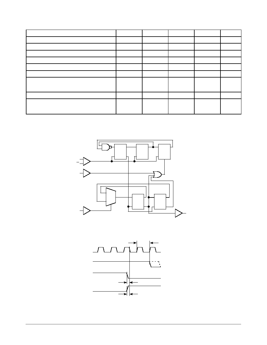
Figure 1. Logic Diagram (MC12026A)
1
0
SW
Figure 2. Modulus Setup Time
Modulus setup time MC to out is the MC
setup or MC release plus the prop delay.
Prop. Delay
In
Out
MC
MC Setup
MC Release

MC12026A
http://onsemi.com
3
Figure 3. AC Test Circuit
SINE WAVE GENERATOR
50
C1
C2
MC INPUT
C3
VCC = 4.5 to 5.5V
CL
RL
VCC
SW
IN
IN
MC
GND
OUT
EXTERNAL COMPONENTS
C1 = C2 = 1000 pF
C3 = 0.1
µ
F
CL = 8pF (Including Scope and Jig Capacitance)
RL = 560
(for
˜
8/9 at 1.1GHz)
………………………………………
………………………………………
………………………………………
………………………………………
………………………………………
0
200
400
600
800
1000
1200
1400
1600
1800
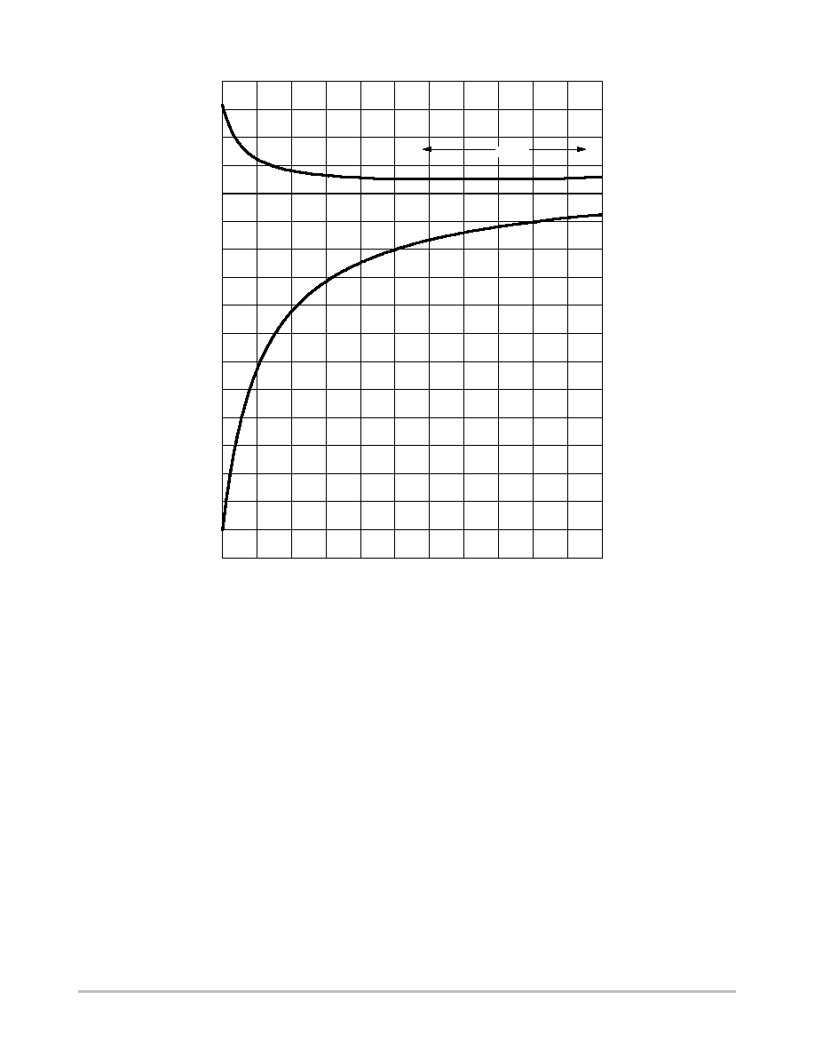
Figure 4. Input Signal Amplitude versus Input Frequency
+15.0
+10.0
+5.0
0
-5.0
-10.0
-15.0
-20.0
-25.0
-30.0
-35.0
-40.0
-45.0
-50.0
+1257.40
+0.71
+1.26
+2.24
+3.98
+7.07
+12.57
+22.36
+39.76
+70.71
+125.74
+223.61
+397.64
+707.11
0
200
400
600
800
1000
1200
1400
1600
1800
FREQUENCY (MHz)
AMPLITUDE (dBm)
mV
rms
FREQUENCY (MHz)
0
400
800
1200
1600
2000
mVpp
Figure 5. Output Amplitude versus Input Frequency
OPERATING
WINDOW
Divide Ratio = 8; VCC = 5.0 V; TA = 25
∞
C
MC12026A
http://onsemi.com
4
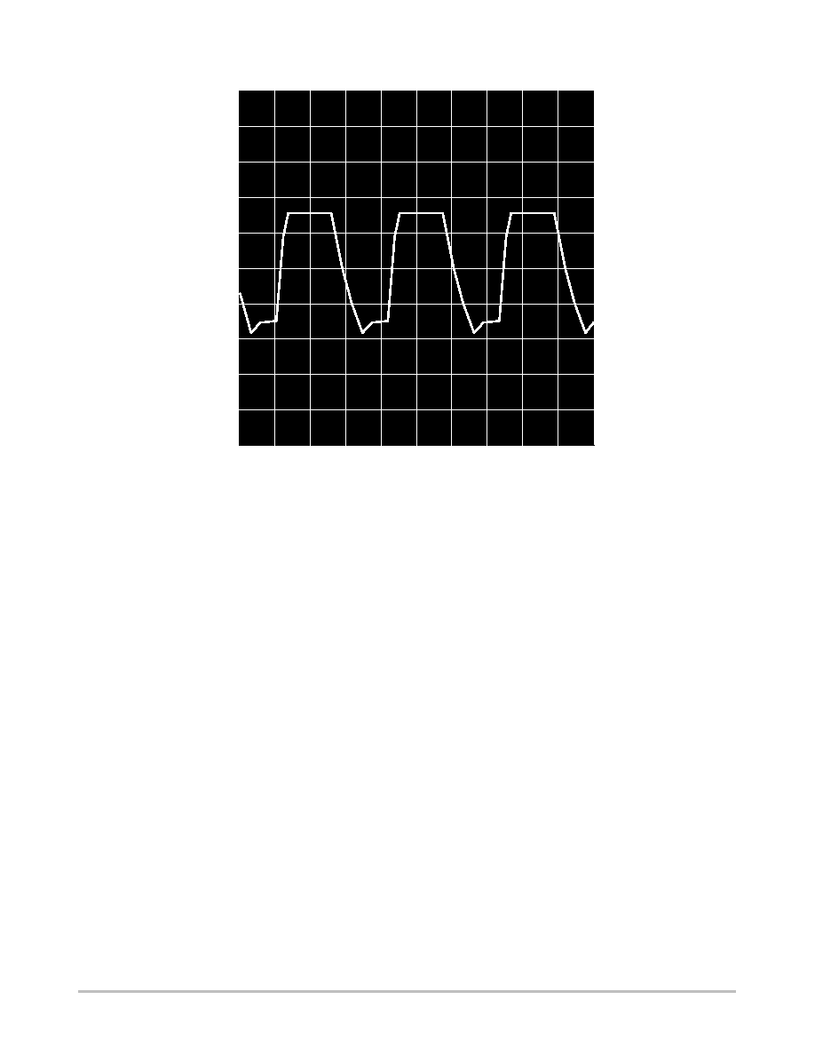
Figure 6. Typical Output Waveform
880mV
36.6ns
86.6ns
5.88V
(
˜
8, 1.1 GHz Input Frequency, VCC = 5.0, TA = 25
∞
C, Output Loaded With 8.0pF)