 | –≠–ª–µ–∫—Ç—Ä–æ–Ω–Ω—ã–π –∫–æ–º–ø–æ–Ω–µ–Ω—Ç: MC74AC377 | –°–∫–∞—á–∞—Ç—å:  PDF PDF  ZIP ZIP |
©
Semiconductor Components Industries, LLC, 2001
May, 2001 ≠ Rev.6
1
Publication Order Number:
MC74AC377/D
MC74AC377, MC74ACT377
Octal D Flip-Flop with
Clock Enable
The MC74AC377/74ACT377 has eight edge-triggered, D-type
flip-flops with individual D inputs and Q outputs. The common
buffered Clock (CP) input loads all flip-flops simultaneously, when
the Clock Enable (CE) is LOW. The register is fully edge-triggered.
The state of each D input, one setup time before the LOW-to-HIGH
clock transition, is transferred to the corresponding flip-flop's Q
output. The CE input must be stable only one setup time prior to the
LOW-to-HIGH clock transition for predictable operation.
∑
Ideal for Addressable Register Applications
∑
Clock Enable for Address and Data Synchronization Applications
∑
Eight Edge-Triggered D Flip-Flops
∑
Buffered Common Clock
∑
Outputs Source/Sink 24 mA
∑
See MC74AC273 for Master Reset Version
∑
See MC74AC373 for Transparent Latch Version
∑
See MC74AC374 for 3-State Version
∑
ACT377 Has TTL Compatible Inputs
∑
MSL = 1 for all Surface Mount
∑
Chip Complexity: 292 FETS or 73 Gates
http://onsemi.com
1
20
PDIP≠20
N SUFFIX
CASE 738
1
20
1
20
1
20
SO≠20
DW SUFFIX
CASE 751
TSSOP≠20
DT SUFFIX
CASE 948E
EIAJ≠20
M SUFFIX
CASE 967
See general marking information in the device marking
section on page 8 of this data sheet.
DEVICE MARKING INFORMATION
See detailed ordering and shipping information in the package
dimensions section on page 7 of this data sheet.
ORDERING INFORMATION

MC74AC377, MC74ACT377
http://onsemi.com
2
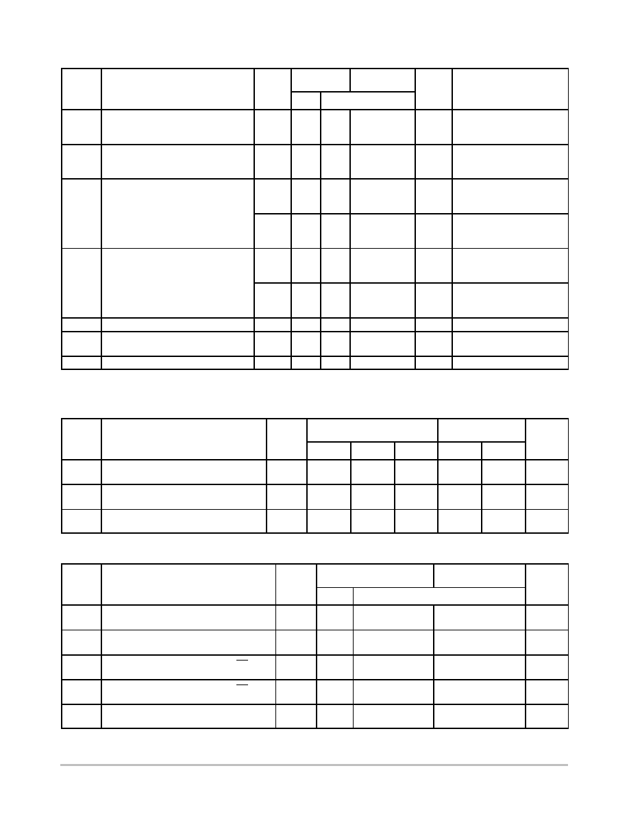
19
20
18
17
16
15
14
2
1
3
4
5
6
7
VCC
13
8
12
9
11
10
O7
D7
D6
O6
O5
D5
D4
O4
CP
CE
O0
D0
D1
O1
O2
D2
D3
O3
GND
Figure 1. Pinout: 20≠Lead Packages Conductors
(Top View)
Figure 2. LOGIC SYMBOL
O0 O1 O2 O3 O4 O5 O6 O7
D0 D1 D2 D3 D4 D5 D6 D7
CP
CE
PIN NAMES
PIN
FUNCTION
D0≠D7
Data Inputs
CE
Clock Enable (Active LOW)
Q0≠Q7
Data Outputs
CP
Clock Pulse Input
MODE SELECT-FUNCTION TABLE
Operating Mode
Inputs
Outputs
Operating Mode
CP
CE
Dn
Qn
Load
1
L
H
H
Load
0
L
L
L
Hold (Do Nothing)
H
X
No Change
Hold (Do Nothing)
X
H
X
No Change
H = HIGH Voltage Level
L = LOW Voltage Level
X = Immaterial
= LOW-to-HIGH Clock Transition
Please note that this diagram is provided only for the understanding of logic
operations and should not be used to estimate propagation delays.
Figure 3. LOGIC DIAGRAM
D
Q
CP
D
Q
CP
D
Q
CP
D
Q
CP
D
Q
CP
D
Q
CP
D
Q
CP
D
Q
CP
D0
D1
D2
D3
D4
D5
D6
D7
O0
O1
O2
O3
O4
O5
O6
O7
CE
CP
MC74AC377, MC74ACT377
http://onsemi.com
3
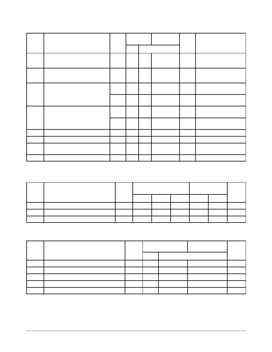
MAXIMUM RATINGS*
Symbol
Parameter
Value
Unit
VCC
DC Supply Voltage (Referenced to GND)
≠0.5 to +7.0
V
Vin
DC Input Voltage (Referenced to GND)
≠0.5 to VCC +0.5
V
Vout
DC Output Voltage (Referenced to GND)
≠0.5 to VCC +0.5
V
Iin
DC Input Current, per Pin
±
20
mA
Iout
DC Output Sink/Source Current, per Pin
±
50
mA
ICC
DC VCC or GND Current per Output Pin
±
50
mA
Tstg
Storage Temperature
≠65 to +150
∞
C
JA
Thermal Resistance (Junction to Ambient)
SOIC, DW
TSSOP, DT
PDIP, N
97
129
69
∞
C/W
VESD
ESD Withstand Voltage
Human Body Model (Note 1)
Machine Model (Note 2)
Charged Device Model (Note 3)
> 2000
> 200
> 1000
V
ILatch≠Up Latch≠Up Performance
VCC = 5.5 V; TA = 125
∞
C (Note 4)
> 100
mA
* Maximum Ratings are those values beyond which damage to the device may occur. Functional operation should be restricted to the
Recommended Operating Conditions.
1. Tested to EIA/JESD22≠A114≠A
2. Tested to EIA/JESD22≠A115≠A
3. Tested to JESD22≠C101≠A
4. Tested to EIA/JESD78
RECOMMENDED OPERATING CONDITIONS
Symbol
Parameter
Min
Typ
Max
Unit
VCC
Supply Voltage
AC
2.0
5.0
6.0
V
VCC
Supply Voltage
ACT
4.5
5.0
5.5
V
Vin, Vout
DC Input Voltage, Output Voltage (Ref. to GND)
0
VCC
V
I
t Ri
d F ll Ti
(N t 5)
VCC @ 3.0 V
150
tr, tf
Input Rise and Fall Time (Note 5)
AC Devices except Schmitt Inputs
VCC @ 4.5 V
40
ns/V
r, f
AC Devices exce t Schmitt In uts
VCC @ 5.5 V
25
t tf
Input Rise and Fall Time (Note 6)
VCC @ 4.5 V
10
ns/V
tr, tf
In ut Rise and Fall Time (Note 6)
ACT Devices except Schmitt Inputs
VCC @ 5.5 V
8.0
ns/V
TJ
Junction Temperature (PDIP)
140
∞
C
TA
Operating Ambient Temperature Range
≠40
25
85
∞
C
IOH
Output Current -- High
≠24
mA
IOL
Output Current -- Low
24
mA
5. Vin from 30% to 70% VCC; see individual Data Sheets for devices that differ from the typical input rise and fall times.
6. Vin from 0.8 V to 2.0 V; see individual Data Sheets for devices that differ from the typical input rise and fall times.
MC74AC377, MC74ACT377
http://onsemi.com
4
74AC ≠ DC CHARACTERISTICS
TA = +25
∞
C
TA =
TA = +25 C
TA =
≠40
∞
C to +85
∞
C
Symbol
Parameter
VCC (V)
Typ
Guaranteed Limits
Unit
Conditions
VIH
Minimum High Level Input Voltage
3.0
4.5
5.5
1.50
2.25
2.75
2.10
3.15
3.85
2.10
3.15
3.85
V
V
V
VOUT = 0.1 V
or
VCC ≠ 0.1 V
VIL
Maximum Low Level Input Voltage
3.0
4.5
5.5
1.50
2.25
2.75
0.90
1.35
1.65
0.90
1.35
1.65
V
V
V
VOUT = 0.1 V
or
VCC ≠ 0.1 V
VOH
Minimum High Level Output Voltage
3.0
4.5
5.5
2.99
4.49
5.49
2.9
4.4
5.4
2.9
4.4
5.4
V
V
V
IOUT = ≠50
µ
A
3.0
4.5
5.5
2.56
3.86
4.86
2.46
3.76
4.76
V
V
V
*VIN = VIL or VIH
≠12 mA
IOH
≠24 mA
≠24 mA
VOL
Maximum Low Level Output Voltage
3.0
4.5
5.5
0.002
0.001
0.001
0.1
0.1
0.1
0.1
0.1
0.1
V
V
V
IOUT = 50
µ
A
3.0
4.5
5.5
0.36
0.36
0.36
0.44
0.44
0.44
V
V
V
*VIN = VIL or VIH
≠12 mA
IOH
≠24 mA
≠24 mA
IIN
Maximum Input Leakage Current
5.5
±
0.1
±
1.0
µ
A
VI = VCC, GND
IOLD
IOHD
Maximum Input Leakage Current
5.5
5.5
75
≠75
mA
mA
VOLD = 1.65 V Max
VOHD = 3.85 V Min
ICC
Maximum Quiescent Supply Current
5.5
8.0
80
µ
A
VIN = VCC or GND
*All outputs loaded; thresholds on input associated with output under test.
Maximum test duration 2.0 ms, one output loaded at a time.
NOTE:
IIN and ICC @ 3.0 V are guaranteed to be less than or equal to the respective limit @ 5.5 V VCC.
74AC ≠ AC CHARACTERISTICS
For Figures and Waveforms, See Figures 4, 5, and 6.
TA = +25
∞
C
TA = ≠40
∞
C to +85
∞
C
TA = +25 C
CL = 50 pF
TA = 40 C to +85 C
CL = 50 pF
Symbol
Parameter
VCC* (V)
Min
Typ
Max
Min
Max
Unit
fmax
Maximum Clock Frequency
3.3
5.0
90
140
75
125
MHz
tPLH
Propagation Delay
CP to Qn
3.3
5.0
3.0
2.0
13.0
9.0
1.5
1.5
14.0
10.0
ns
tPHL
Propagation Delay
CP to Qn
3.3
5.0
3.5
2.5
13.0
10.0
2.0
1.5
14.5
11.0
ns
* Voltage Range 3.3 V is 3.3 V
±
0.3 V; Voltage Range 5.0 V is 5.0 V
±
0.5 V.
74AC ≠ AC OPERATING REQUIREMENTS
TA = +25
∞
C
TA = ≠40
∞
C to +85
∞
C
TA = +25 C
CL = 50 pF
TA = 40 C to +85 C
Symbol
Parameter
VCC* (V)
Typ
Guaranteed Minimum
Unit
ts
Setup Time, HIGH or LOW
Dn to CP
3.3
5.0
5.5
4.0
6.0
4.5
ns
th
Hold Time, HIGH or LOW
Dn to CP
3.3
5.0
0
1.0
0
1.0
ns
ts
Setup Time, HIGH or LOW
CE to CP
3.3
5.0
6.0
4.0
7.5
4.5
ns
th
Hold Time, HIGH or LOW
CE to CP
3.3
5.0
0
1.0
0
1.0
ns
tw
CP Pulse Width
HIGH or LOW
3.3
5.0
5.5
4.0
6.0
4.5
ns
* Voltage Range 3.3 V is 3.3 V
±
0.3 V; Voltage Range 5.0 V is 5.0 V
±
0.5 V.
MC74AC377, MC74ACT377
http://onsemi.com
5
74ACT ≠ DC CHARACTERISTICS
TA =
TA = +25
5
C
TA =
≠40
5
C to +85
5
C
Symbol
Parameter
VCC (V)
Typ
Guaranteed Limits
Unit
Conditions
VIH
Minimum High Level Input Voltage
4.5
5.5
1.5
1.5
2.0
2.0
2.0
2.0
V
VOUT = 0.1 V
or
VCC ≠ 0.1 V
VIL
Maximum Low Level Input Voltage
4.5
5.5
1.5
1.5
0.8
0.8
0.8
0.8
V
VOUT = 0.1 V
or
VCC ≠ 0.1 V
VOH
Minimum High Level Output Voltage
4.5
5.5
4.49
5.49
4.4
5.4
4.4
5.4
V
IOUT = ≠50
µ
A
4.5
5.5
3.86
4.86
3.76
4.76
V
*VIN = VIL or VIH
≠24 mA
IOH
≠24 mA
VOL
Maximum Low Level Output Voltage
4.5
5.5
0.001
0.001
0.1
0.1
0.1
0.1
V
IOUT = 50
µ
A
4.5
5.5
0.36
0.36
0.44
0.44
V
*VIN = VIL or VIH
≠24 mA
IOH
≠24 mA
IIN
Maximum Input Leakage Current
5.5
±
0.1
±
1.0
µ
A
VI = VCC, GND
ICCT
Additional Max. ICC/Input
5.5
0.6
1.5
mA
VI = VCC ≠ 2.1 V
IOLD
IOHD
Minimum Dynamic Output Current
5.5
75
≠75
mA
VOLD = 1.65 V Max
VOHD = 3.85 V Min
ICC
Maximum Quiescent Supply Current
5.5
8.0
80
µ
A
VIN = VCC or GND
*All outputs loaded; thresholds on input associated with output under test.
Maximum test duration 2.0 ms, one output loaded at a time.
74ACT ≠ AC CHARACTERISTICS
For Figures and Waveforms -- See Figures 4, 5, and 6.
TA = +25
∞
C
TA = ≠40
∞
C to +85
∞
C
TA = +25 C
CL = 50 pF
TA = 40 C to +85 C
CL = 50 pF
Symbol
Parameter
VCC* (V)
Min
Typ
Max
Min
Max
Unit
fmax
Maximum Clock Frequency
5.0
140
125
MHz
tPLH
Propagation Delay
CP to Qn
5.0
3.0
9.0
2.5
10
ns
tPHL
Propagation Delay
CP to Qn
5.0
3.5
10
2.5
11
ns
*Voltage Range 5.0 V is 5.0 V
±
0.5 V.
74ACT ≠ AC OPERATING REQUIREMENTS
TA = +25
∞
C
TA = ≠40
∞
C to +85
∞
C
TA = +25 C
CL = 50 pF
TA = ≠40 C to +85 C
CL = 50 pF
Symbol
Parameter
VCC* (V)
Typ
Guaranteed Minimum
Unit
ts
Setup Time, HIGH or LOW
Dn to CP
5.0
4.5
5.5
ns
th
Hold Time, HIGH or LOW
Dn to CP
5.0
1.0
1.0
ns
ts
Setup Time, HIGH or LOW
CE to CP
5.0
4.5
5.5
ns
th
Hold Time, HIGH or LOW
CE to CP
5.0
1.0
1.0
ns
tw
CP Pulse Width
HIGH or LOW
5.0
4.0
4.5
ns
*Voltage Range 5.0 V is 5.0 V
±
0.5 V.