
й
Semiconductor Components Industries, LLC, 2001
May, 2001 н Rev. 5
1
Publication Order Number:
MC74AC132/D
MC74AC132, MC74ACT132
Quad 2-Input NAND Schmitt
Trigger
The MC74AC/74ACT132 contains four 2нinput NAND gates
which are capable of transforming slowly changing input signals into
sharply defined, jitterнfree output signals. In addition, they have
greater noise margin than conventional NAND gates.
Each circuit contains a 2нinput Schmitt trigger. The Schmitt
trigger uses positive feedback to effectively speedнup slow input
transitions, and provide different input threshold voltages for
positive and negative-going transitions. This hysteresis between the
positiveнgoing and negativeнgoing input threshold is determined by
resistor ratios and is essentially insensitive to temperature and supply
voltage variations.
╖
Schmitt Trigger Inputs
╖
Outputs Source/Sink 24 mA
╖
ACT132 Has TTL Compatible Inputs
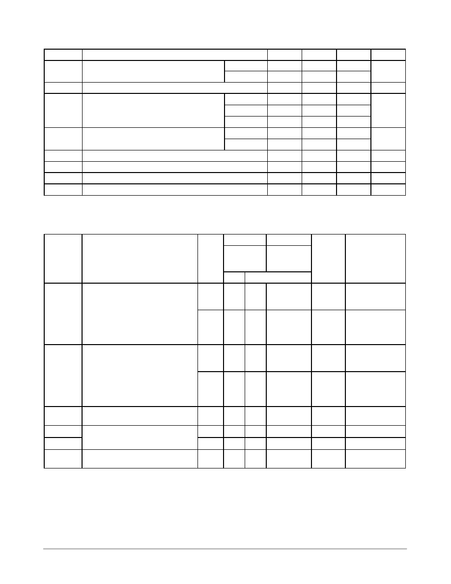
13
14
12
11
10
9
8
2
1
3
4
5
6
7
GND
VCC
Figure 1. Pinout; 14нLead Packages Conductors
(Top View)
FUNCTION TABLE
Inputs
Output
A
B
Y
L
L
H
L
H
H
H
L
H
H
H
L
H = HIGH Voltage Level
L = LOW Voltage Level
TSSOPн14
DT SUFFIX
CASE 948G
1
14
EIAJн14
M SUFFIX
CASE 965
1
14
SOн14
D SUFFIX
CASE 751A
http://onsemi.com
1
14
1
14
PDIPн14
N SUFFIX
CASE 646
Device
Package
Shipping
ORDERING INFORMATION
MC74AC132DT
TSSOPн14
96 Units/Rail
MC74AC132DTR2
TSSOPн14 2500 Tape & Reel
MC74ACT132DT
TSSOPн14
96 Units/Rail
MC74ACT132DTR2 TSSOPн14 2500 Tape & Reel
MC74AC132N
PDIPн14
25 Units/Rail
MC74AC132D
SOICн14
55 Units/Rail
MC74ACT132N
PDIPн14
25 Units/Rail
MC74AC132DR2
SOICн14
2500 Tape & Reel
MC74ACT132D
SOICн14
55 Units/Rail
MC74ACT132DR2
SOICн14
2500 Tape & Reel
MC74AC132M
EIAJн14
50 Units/Rail
MC74AC132MEL
EIAJн14
2000 Tape & Reel
MC74ACT132M
EIAJн14
50 Units/Rail
MC74ACT132MEL
EIAJн14
2000 Tape & Reel
See general marking information in the device marking
section on page 5 of this data sheet.
DEVICE MARKING INFORMATION
MC74AC132, MC74ACT132
http://onsemi.com
2
RECOMMENDED OPERATING CONDITIONS
Symbol
Parameter
Min
Typ
Max
Unit
V
Supply Voltage
AC
2.0
5.0
6.0
V
VCC
Supply Voltage
ACT
4.5
5.0
5.5
V
Vin, Vout
DC Input Voltage, Output Voltage (Ref. to GND)
0
н
VCC
V
VCC @ 3.0 V
н
150
н
tr, tf
Input Rise and Fall Time (Note 1)
AC Devices except Schmitt Inputs
VCC @ 4.5 V
н
40
н
ns/V
r, f
AC Devices except Schmitt Inputs
VCC @ 5.5 V
н
25
н
t tf
Input Rise and Fall Time (Note 2)
VCC @ 4.5 V
н
10
н
ns/V
tr, tf
In ut Rise and Fall Time (Note 2)
ACT Devices except Schmitt Inputs
VCC @ 5.5 V
н
8.0
н
ns/V
TJ
Junction Temperature (PDIP)
н
н
140
░
C
TA
Operating Ambient Temperature Range
н40
25
85
░
C
IOH
Output Current н High
н
н
н24
mA
IOL
Output Current н Low
н
н
24
mA
1. Vin from 30% to 70% VCC; see individual Data Sheets for devices that differ from the typical input rise and fall times.
2. Vin from 0.8 V to 2.0 V; see individual Data Sheets for devices that differ from the typical input rise and fall times.
DC CHARACTERISTICS
74AC
74AC
Symbol
Parameter
VCC
(V)
TA = +25
░
C
TA =
н40
░
C to
+85
░
C
Unit
Conditions
Typ
Guaranteed Limits
VOH
Minimum High Level
3.0
2.99
2.9
2.9
IOUT = н50
╡
A
g
Output Voltage
4.5
4.49
4.4
4.4
V
5.5
5.49
5.4
5.4
*VIN = VIL or VIH
3.0
н
2.56
2.46
V
н12 mA
4.5
н
3.86
3.76
V
IOH
н24 mA
5.5
н
4.86
4.76
н24 mA
VOL
Maximum Low Level
3.0
0.002
0.1
0.1
IOUT = 50
╡
A
Output Voltage
4.5
0.001
0.1
0.1
V
5.5
0.001
0.1
0.1
*VIN = VIL or VIH
3.0
н
0.36
0.44
V
12 mA
4.5
н
0.36
0.44
V
IOL
24 mA
5.5
н
0.36
0.44
24 mA
IIN
Maximum Input
5 5
н
▒
0 1
▒
1 0
╡
A
VI = VCC GND
Leakage Current
5.5
н
▒
0.1
▒
1.0
╡
A
VI = VCC, GND
IOLD
Minimum Dynamic
O t
t C
t
5.5
н
н
75
mA
VOLD = 1.65 V Max
IOHD
Output Current
5.5
н
н
н75
mA
VOHD = 3.85 V Min
ICC
Maximum Quiescent
5 5
н
4 0
40
╡
A
VIN = VCC or GND
Q
Supply Current
5.5
4.0
40
╡
A
VIN = VCC or GND
*All outputs loaded; thresholds on input associated with output under test.
Maximum test duration 2.0 ms, one output loaded at a time.
NOTE:
IIN and ICC @ 3.0 V are guaranteed to be less than or equal to the respective limit @ 5.5 V VCC.

MC74AC132, MC74ACT132
http://onsemi.com
3
AC CHARACTERISTICS
(For Figures and Waveforms н See Section 3 of the ON Semiconductor FACT Data Book, DL138/D)
74AC
74AC
Symbol
Parameter
VCC*
(V)
TA = +25
░
C
CL = 50 pF
TA = н40
░
C
to +85
░
C
CL = 50 pF
Unit
Fig.
No.
Min
Typ
Max
Min
Max
tPLH
Propagation Delay
3.3
2.0
н
13.0
1.5
14.0
ns
3н5
tPLH
Propagation Delay
5.0
2.0
н
9.0
1.5
10.0
ns
3н5
tPHL
Propagation Delay
3.3
2.0
н
13.5
1.5
15.0
ns
3н5
tPHL
Propagation Delay
5.0
2.0
н
9.0
1.5
10.0
ns
3н5
*Voltage Range 3.3 V is 3.3 V
▒
0.3 V.
Voltage Range 5.0 V is 5.0 V
▒
0.5 V.
DC CHARACTERISTICS
74ACT
74ACT
Symbol
Parameter
VCC
(V)
TA = +25
░
C
TA =
н40
░
C to
+85
░
C
Unit
Conditions
Typ
Guaranteed Limits
VOH
Minimum High Level
4.5
4.49
4.4
4.4
V
IOUT = н50
╡
A
g
Output Voltage
5.5
5.49
5.4
5.4
V
*VIN = VIL or VIH
4.5
н
3.86
3.76
V
IOH
н24 mA
5.5
н
4.86
4.76
IOH
н24 mA
VOL
Maximum Low Level
4.5
0.001
0.1
0.1
V
IOUT = 50
╡
A
Output Voltage
5.5
0.001
0.1
0.1
V
*VIN = VIL or VIH
4.5
н
0.36
0.44
V
IOL
24 mA
5.5
н
0.36
0.44
IOL
24 mA
IIN
Maximum Input
5 5
н
▒
0 1
▒
1 0
╡
A
VI = VCC GND
Leakage Current
5.5
н
▒
0.1
▒
1.0
╡
A
VI = VCC, GND
ICCT
Additional Max. ICC/Input
5.5
0.6
н
1.5
mA
VI = VCC н 2.1 V
IOLD
Minimum Dynamic
O t
t C
t
5.5
н
н
75
mA
VOLD = 1.65 V Max
IOHD
Output Current
5.5
н
н
н75
mA
VOHD = 3.85 V Min
ICC
Maximum Quiescent
5 5
н
4 0
40
╡
A
VIN = VCC or GND
Q
Supply Current
5.5
н
4.0
40
╡
A
VIN = VCC or GND
*All outputs loaded; thresholds on input associated with output under test.
Maximum test duration 2.0 ms, one output loaded at a time.
AC CHARACTERISTICS
(For Figures and Waveforms н See Section 3 of the ON Semiconductor FACT Data Book, DL138/D)
74ACT
74ACT
Symbol
Parameter
VCC*
(V)
TA = +25
░
C
CL = 50 pF
TA = н40
░
C
to +85
░
C
CL = 50 pF
Unit
Fig.
No.
Min
Typ
Max
Min
Max
tPLH
Propagation Delay
5.0
3.0
н
11.5
2.5
13.0
ns
3н6
tPHL
Propagation Delay
5.0
3.0
н
11.0
2.5
12.5
ns
3н5
*Voltage Range 5.0 V is 5.0 V
▒
0.5 V.
MC74AC132, MC74ACT132
http://onsemi.com
4
INPUT CHARACTERISTICS (unless otherwise specified)
Symbol
Parameter
VCC
(V)
74AC
74ACT
Unit
Test Conditions
Maximum Positive
3.0
2.2
Vt +
Maximum Positive
Threshold
4.5
3.2
2.0
V
TA = Worst Case
Threshold
5.5
3.9
Minimum Negative
3.0
0.5
Vt н
Minimum Negative
Threshold
4.5
0.9
0.8
V
TA = Worst Case
Threshold
5.5
1.1
3.0
1.2
Vh(max)
Maximum Hysteresis
4.5
1.4
1.2
V
TA = Worst Case
5.5
1.6
3.0
0.3
Vh(min)
Minimum Hysteresis
4.5
0.4
0.4
V
TA = Worst Case
5.5
0.5
CAPACITANCE
Symbol
Parameter
Value
Typ
Unit
Test Conditions
CIN
Input Capacitance
4.5
pF
VCC = 5.0 V
CPD
Power Dissipation Capacitance
30
pF
VCC = 5.0 V
MC74AC132, MC74ACT132
http://onsemi.com
5
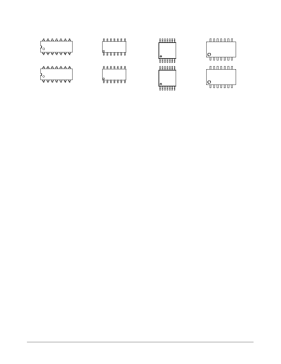
MARKING DIAGRAMS
A
= Assembly Location
WL, L
= Wafer Lot
YY, Y
= Year
WW, W = Work Week
PDIPн14
SOн14
TSSOPн14
MC74AC132N
AWLYYWW
AC132
AWLYWW
AC
132
ALYW
ACT
132
ALYW
ACT132
AWLYWW
MC74ACT132N
AWLYYWW
74AC132
ALYW
EIAJн14
74ACT132
ALYW