©
Semiconductor Components Industries, LLC, 1999
November, 1999 ≠ Rev. 1
1
Publication Order Number:
MC74VHC1G66/D
MC74VHC1G66
Advance Information
Analog Switch
The MC74VHC1G66 is an advanced high speed CMOS bilateral
analog switch fabricated with silicon gate CMOS technology. It
achieves high speed propagation delays and low ON resistances while
maintaining CMOS low power dissipation. This bilateral switch
controls analog and digital voltages that may vary across the full
power≠supply range (from VCC to GND).
The MC74VHC1G66 is compatible in function to a single gate of
the High Speed CMOS MC74VHC4066 and the metal≠gate CMOS
MC14066. The device has been designed so that the ON resistances
(RON) are much lower and more linear over input voltage than RON of
the metal≠gate CMOS or High Speed CMOS analog switches.
The ON/OFF control inputs are compatible with standard CMOS
outputs; with pull≠up resistors, it is compatible with LSTTL outputs.
∑
High Speed: tPD = TBD (Typ) at VCC = 5 V
∑
Low Power Dissipation: ICC = 2 mA (Max) at TA = 25
∞
C
∑
Diode Protection Provided on Inputs and Outputs
∑
Improved Linearity and Lower ON Resistance over Input Voltage
than the MC14066 or the HC4066
∑
Pin and Function Compatible with Other Standard Logic Families
∑
Latchup Performance Exceeds 300 mA
∑
ESD Performance: HBM > 2000 V; MM > 200 V, CDM > 1500 V
∑
Chip Complexity: 11 FETs or 3 Equivalent Gates
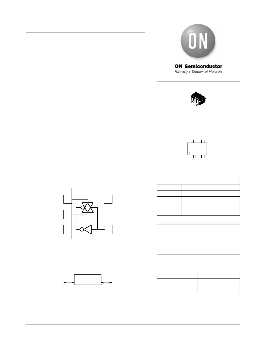
5
1
2
4
3
VCC
IN/OUT XA
OUT/IN YA
ON/OFF CONTROL
GND
5≠Lead SOT≠353 Pinout (Top View)
ON/OFF CONTROL
OUT/IN YA
1
U
U
IN/OUT XA
1
X 1
LOGIC SYMBOL
This document contains information on a new product. Specifications and information
herein are subject to change without notice.
SC≠88A / SOT≠353
DF SUFFIX
CASE 419A
PIN ASSIGNMENT
1
2
3
GND
IN/OUT XA
OUT/IN YA
http://onsemi.com
Pin 1
d = Date Code
V9d
4
5
VCC
ON/OFF CONTROL
FUNCTION TABLE
MARKING DIAGRAM
See detailed ordering and shipping information in the package
dimensions section on page 7 of this data sheet.
ORDERING INFORMATION
L
H
On/Off Control Input
State of Analog Switch
Off
On
MC74VHC1G66
http://onsemi.com
2
ABSOLUTE MAXIMUM RATINGS
Characteristics
Symbol
Value
Unit
DC Supply Voltage
VCC
≠0.5 to +7.0
V
Digital Input Voltage
VIN
≠0.5 to VCC +0.5
V
Analog Output Voltage
VIS
≠0.5 to VCC + 0.5
V
Digital Input Diode Current
IIK
≠20
mA
DC Supply Current, VCC and GND
ICC
+25
mA
Power dissipation in still air, SC≠88A
PD
200
mW
Lead temperature, 1 mm from case for 10 s
TL
260
∞
C
Storage temperature
Tstg
≠65 to +150
∞
C
Derating -- SC≠88A Package: ≠3 mW/
_
C from 65
_
to 125
_
C
RECOMMENDED OPERATING CONDITIONS
Characteristics
Symbol
Min
Max
Unit
DC Supply Voltage
VCC
4.5
5.5
V
Digital Input Voltage
VIN
GND
VCC
V
Analog Input Voltage
VIS
GND
VCC
V
Static or Dynamic Voltage Across Switch
VIO*
1.2
V
Operating Temperature Range
TA
≠55
+85
∞
C
Input Rise and Fall Time
ON/OFF Control Input
VCC = 3.3V
±
0.3V
VCC = 5.0V
±
0.5V
tr , tf
0
0
100
20
ns/V
* For voltage drops across the switch greater than 1.2V (switch on), excessive VCC current may be drawn; i.e. the current out of the switch may
contain both VCC and switch input components. The reliability of the device will be unaffected unless the Maximum Ratings are exceeded.
MC74VHC1G66
http://onsemi.com
3
DC ELECTRICAL CHARACTERISTICS
VCC
TA = 25
∞
C
TA
85
∞
C
TA
125
∞
C
Symbol
Parameter
Test Conditions
(V)
Min
Typ
Max
Min
Max
Min
Max
Unit
VIH
Minimum High≠Level
Input Voltage
ON/OFF Control Input
RON = Per Spec
2.0
3.0
4.5
5.5
1.5
2.1
3.15
3.85
1.5
2.1
3.15
3.85
1.5
2.1
3.15
3.85
V
VIL
Maximum Low≠Level
Input Voltage
ON/OFF Control Input
RON = Per Spec
2.0
3.0
4.5
5.5
0.5
0.9
1.35
1.65
0.5
0.9
1.35
1.65
0.5
0.9
1.35
1.65
V
IIN
Maximum Input
Leakage Current
ON/OFF Control Input
VIN = VCC or GND
0 to
5.5
±
0.1
±
1.0
±
1.0
µ
A
ICC
Maximum Quiescent
Supply Current
VIN = VCC or GND
VIO = 0V
5.5
2.0
20
40
µ
A
RON
Maximum "ON"
Resistance
VIN = VIH
VIS = VCC or GND
|IIS|
10mA (Figure 1)
3.0
4.5
5.5
30
20
15
50
30
20
70
40
35
100
50
45
W
Endpoints
VIN = VIH
VIS = VCC or GND
|IIS|
10mA (Figure 1)
3.0
4.5
5.5
25
12
8
50
20
15
65
26
23
90
40
32
W
IOFF
Maximum Off≠Channel
Leakage Current
VIN = VIL
VIS = VCC or GND
Switch Off (Figure 2)
5.5
0.1
0.5
1.0
µ
A
ION
Maximum On≠Channel
Leakage
Current
VIN = VIH
VIS = VCC or GND
Switch On (Figure 3)
5.5
0.1
0.5
1.0
µ
A
ŒŒŒŒŒŒŒŒŒŒŒŒŒŒŒŒŒŒŒŒŒŒŒŒŒŒŒŒŒŒŒŒŒ
ŒŒŒŒŒŒŒŒŒŒŒŒŒŒŒŒŒŒŒŒŒŒŒŒŒŒŒŒŒŒŒŒŒ
AC ELECTRICAL CHARACTERISTICS
(Cload = 50 pF, Input tr/tf = 3.0ns)
ŒŒŒŒ
ŒŒŒŒ
ŒŒŒŒŒŒŒ
ŒŒŒŒŒŒŒ
ŒŒŒŒŒŒŒ
ŒŒŒŒŒŒŒ
ŒŒŒ
ŒŒŒ
VCC
ŒŒŒŒŒŒŒ
ŒŒŒŒŒŒŒ
TA = 25
∞
C
ŒŒŒŒŒ
ŒŒŒŒŒ
TA
85
∞
C
ŒŒŒŒŒ
ŒŒŒŒŒ
TA
125
∞
C
ŒŒ
ŒŒ
ŒŒŒŒ
ŒŒŒŒ
Symbol
ŒŒŒŒŒŒŒ
ŒŒŒŒŒŒŒ
Parameter
ŒŒŒŒŒŒŒ
ŒŒŒŒŒŒŒ
Test Conditions
ŒŒŒ
ŒŒŒ
VCC
(V)
ŒŒŒ
ŒŒŒ
Min
ŒŒŒ
ŒŒŒ
Typ
ŒŒŒ
ŒŒŒ
Max
ŒŒŒ
ŒŒŒ
Min
ŒŒŒ
ŒŒŒ
Max
ŒŒŒ
ŒŒŒ
Min
ŒŒŒ
ŒŒŒ
Max
ŒŒ
ŒŒ
Unit
ŒŒŒŒ
Œ
ŒŒ
Œ
Œ
ŒŒ
Œ
ŒŒŒŒ
tPLH,
tPHL
ŒŒŒŒŒŒŒ
Œ
ŒŒŒŒŒ
Œ
Œ
ŒŒŒŒŒ
Œ
ŒŒŒŒŒŒŒ
Maximum Propogation
Delay,
Input X to Y
ŒŒŒŒŒŒŒ
Œ
ŒŒŒŒŒ
Œ
Œ
ŒŒŒŒŒ
Œ
ŒŒŒŒŒŒŒ
YA = Open
Figure 4
ŒŒŒ
Œ
Œ
Œ
Œ
Œ
Œ
ŒŒŒ
2.0
3.0
4.5
5.5
ŒŒŒ
Œ
Œ
Œ
Œ
Œ
Œ
ŒŒŒ
ŒŒŒ
Œ
Œ
Œ
Œ
Œ
Œ
ŒŒŒ
1
0
0
0
ŒŒŒ
Œ
Œ
Œ
Œ
Œ
Œ
ŒŒŒ
5
2
1
1
ŒŒŒ
Œ
Œ
Œ
Œ
Œ
Œ
ŒŒŒ
ŒŒŒ
Œ
Œ
Œ
Œ
Œ
Œ
ŒŒŒ
6
3
1
1
ŒŒŒ
Œ
Œ
Œ
Œ
Œ
Œ
ŒŒŒ
ŒŒŒ
Œ
Œ
Œ
Œ
Œ
Œ
ŒŒŒ
7
4
2
1
ŒŒ
ŒŒ
ŒŒ
ŒŒ
ns
ŒŒŒŒ
Œ
ŒŒ
Œ
ŒŒŒŒ
tPLZ,
tPHZ
ŒŒŒŒŒŒŒ
Œ
ŒŒŒŒŒ
Œ
ŒŒŒŒŒŒŒ
Maximum Propogation
Delay,
ON/OFF Control to
Analog Output
ŒŒŒŒŒŒŒ
Œ
ŒŒŒŒŒ
Œ
ŒŒŒŒŒŒŒ
RL = 1000
W
Figure 5
ŒŒŒ
Œ
Œ
Œ
ŒŒŒ
2.0
3.0
4.5
5.5
ŒŒŒ
Œ
Œ
Œ
ŒŒŒ
ŒŒŒ
Œ
Œ
Œ
ŒŒŒ
15
8
6
4
ŒŒŒ
Œ
Œ
Œ
ŒŒŒ
35
15
10
7
ŒŒŒ
Œ
Œ
Œ
ŒŒŒ
ŒŒŒ
Œ
Œ
Œ
ŒŒŒ
46
20
13
9
ŒŒŒ
Œ
Œ
Œ
ŒŒŒ
ŒŒŒ
Œ
Œ
Œ
ŒŒŒ
57
25
17
11
ŒŒ
ŒŒ
ŒŒ
ns
ŒŒŒŒ
Œ
ŒŒ
Œ
Œ
ŒŒ
Œ
ŒŒŒŒ
tPZL,
tPZH
ŒŒŒŒŒŒŒ
Œ
ŒŒŒŒŒ
Œ
Œ
ŒŒŒŒŒ
Œ
ŒŒŒŒŒŒŒ
Maximum Propogation
Delay,
ON/OFF Control to
Analog Output
ŒŒŒŒŒŒŒ
Œ
ŒŒŒŒŒ
Œ
Œ
ŒŒŒŒŒ
Œ
ŒŒŒŒŒŒŒ
RL = 1000
W
Figure 5
ŒŒŒ
Œ
Œ
Œ
Œ
Œ
Œ
ŒŒŒ
2.0
3.0
4.5
5.5
ŒŒŒ
Œ
Œ
Œ
Œ
Œ
Œ
ŒŒŒ
ŒŒŒ
Œ
Œ
Œ
Œ
Œ
Œ
ŒŒŒ
15
8
6
4
ŒŒŒ
Œ
Œ
Œ
Œ
Œ
Œ
ŒŒŒ
35
15
10
7
ŒŒŒ
Œ
Œ
Œ
Œ
Œ
Œ
ŒŒŒ
ŒŒŒ
Œ
Œ
Œ
Œ
Œ
Œ
ŒŒŒ
46
20
13
9
ŒŒŒ
Œ
Œ
Œ
Œ
Œ
Œ
ŒŒŒ
ŒŒŒ
Œ
Œ
Œ
Œ
Œ
Œ
ŒŒŒ
57
25
17
11
ŒŒ
ŒŒ
ŒŒ
ŒŒ
ns
ŒŒŒŒ
ŒŒŒŒ
CIN
ŒŒŒŒŒŒŒ
ŒŒŒŒŒŒŒ
Maximum Input
C
it
ŒŒŒŒŒŒŒ
ŒŒŒŒŒŒŒ
ON/OFF Control Input
ŒŒŒ
ŒŒŒ
0.0
ŒŒŒ
ŒŒŒ
ŒŒŒ
ŒŒŒ
3
ŒŒŒ
ŒŒŒ
10
ŒŒŒ
ŒŒŒ
ŒŒŒ
ŒŒŒ
10
ŒŒŒ
ŒŒŒ
ŒŒŒ
ŒŒŒ
10
ŒŒ
ŒŒ
pF
ŒŒŒŒ
Œ
ŒŒ
Œ
Œ
ŒŒ
Œ
ŒŒŒŒ
ŒŒŒŒŒŒŒ
Œ
ŒŒŒŒŒ
Œ
Œ
ŒŒŒŒŒ
Œ
ŒŒŒŒŒŒŒ
Capacitance
ŒŒŒŒŒŒŒ
Œ
ŒŒŒŒŒ
Œ
Œ
ŒŒŒŒŒ
Œ
ŒŒŒŒŒŒŒ
Contol Input = GND
Analog I/O
Feedthrough
ŒŒŒ
Œ
Œ
Œ
Œ
Œ
Œ
ŒŒŒ
5.0
ŒŒŒ
Œ
Œ
Œ
Œ
Œ
Œ
ŒŒŒ
ŒŒŒ
Œ
Œ
Œ
Œ
Œ
Œ
ŒŒŒ
4
4
ŒŒŒ
Œ
Œ
Œ
Œ
Œ
Œ
ŒŒŒ
10
10
ŒŒŒ
Œ
Œ
Œ
Œ
Œ
Œ
ŒŒŒ
ŒŒŒ
Œ
Œ
Œ
Œ
Œ
Œ
ŒŒŒ
10
10
ŒŒŒ
Œ
Œ
Œ
Œ
Œ
Œ
ŒŒŒ
ŒŒŒ
Œ
Œ
Œ
Œ
Œ
Œ
ŒŒŒ
10
10
ŒŒ
ŒŒ
ŒŒ
ŒŒ
Typical @ 25
∞
C, VCC = 5.0V
CPD
Power Dissipation Capacitance (Note NO TAG)
18
pF
1. CPD is defined as the value of the internal equivalent capacitance which is calculated from the operating current consumption without load.
Average operating current can be obtained by the equation: ICC(OPR
)
= CPD
VCC
fin + ICC. CPD is used to determine the no≠load dynamic
power consumption; PD = CPD
VCC2
fin + ICC
VCC.
MC74VHC1G66
http://onsemi.com
4
ŒŒŒŒŒŒŒŒŒŒŒŒŒŒŒŒŒŒŒŒŒŒŒŒŒŒŒŒŒŒŒŒŒ
ŒŒŒŒŒŒŒŒŒŒŒŒŒŒŒŒŒŒŒŒŒŒŒŒŒŒŒŒŒŒŒŒŒ
ADDITIONAL APPLICATION CHARACTERISTICS
(Voltages Referenced to GND Unless Noted)
ŒŒŒŒŒ
Œ
ŒŒŒ
Œ
ŒŒŒŒŒ
Symbol
ŒŒŒŒŒŒŒŒŒ
Œ
ŒŒŒŒŒŒŒ
Œ
ŒŒŒŒŒŒŒŒŒ
Parameter
ŒŒŒŒŒŒŒŒŒŒŒŒŒŒ
Œ
ŒŒŒŒŒŒŒŒŒŒŒŒ
Œ
ŒŒŒŒŒŒŒŒŒŒŒŒŒŒ
Test Conditions
ŒŒŒ
Œ
Œ
Œ
ŒŒŒ
VCC
ŒŒŒŒ
Œ
ŒŒ
Œ
ŒŒŒŒ
Limit
25
∞
C
ŒŒŒ
Œ
Œ
Œ
ŒŒŒ
Unit
ŒŒŒŒŒ
Œ
ŒŒŒ
Œ
ŒŒŒŒŒ
BW
ŒŒŒŒŒŒŒŒŒ
Œ
ŒŒŒŒŒŒŒ
Œ
ŒŒŒŒŒŒŒŒŒ
Maximum On≠Channel
Bandwidth or Minimum
Frequency Response
Figure 7
ŒŒŒŒŒŒŒŒŒŒŒŒŒŒ
Œ
ŒŒŒŒŒŒŒŒŒŒŒŒ
Œ
ŒŒŒŒŒŒŒŒŒŒŒŒŒŒ
fin = 1 MHz Sine Wave
Adjust fin voltage to obtain 0 dBm at VOS
Increase fin = frequency until dB meter reads ≠3dB
RL = 50
W
, CL = 10 pF
ŒŒŒ
Œ
Œ
Œ
ŒŒŒ
3.0
4.5
5.5
ŒŒŒŒ
Œ
ŒŒ
Œ
ŒŒŒŒ
150
175
200
ŒŒŒ
Œ
Œ
Œ
ŒŒŒ
MHz
ŒŒŒŒŒ
Œ
ŒŒŒ
Œ
Œ
ŒŒŒ
Œ
ŒŒŒŒŒ
ISOoff
ŒŒŒŒŒŒŒŒŒ
Œ
ŒŒŒŒŒŒŒ
Œ
Œ
ŒŒŒŒŒŒŒ
Œ
ŒŒŒŒŒŒŒŒŒ
Off≠Channel Feedthrough
Isolation
Figure 8
ŒŒŒŒŒŒŒŒŒŒŒŒŒŒ
Œ
ŒŒŒŒŒŒŒŒŒŒŒŒ
Œ
Œ
ŒŒŒŒŒŒŒŒŒŒŒŒ
Œ
ŒŒŒŒŒŒŒŒŒŒŒŒŒŒ
fin = Sine Wave
Adjust fin voltage to obtain 0 dBm at VIS
fin = 10 kHz, RL = 600
W
, CL = 50 pF
ŒŒŒ
Œ
Œ
Œ
Œ
Œ
Œ
ŒŒŒ
3.0
4.5
5.5
ŒŒŒŒ
Œ
ŒŒ
Œ
Œ
ŒŒ
Œ
ŒŒŒŒ
≠50
≠50
≠50
ŒŒŒ
Œ
Œ
Œ
Œ
Œ
Œ
ŒŒŒ
dB
ŒŒŒŒŒ
Œ
ŒŒŒ
Œ
ŒŒŒŒŒ
ŒŒŒŒŒŒŒŒŒ
Œ
ŒŒŒŒŒŒŒ
Œ
ŒŒŒŒŒŒŒŒŒ
ŒŒŒŒŒŒŒŒŒŒŒŒŒŒ
Œ
ŒŒŒŒŒŒŒŒŒŒŒŒ
Œ
ŒŒŒŒŒŒŒŒŒŒŒŒŒŒ
fin = 1.0 kHz, RL = 50
W
, CL = 10 pF
ŒŒŒ
Œ
Œ
Œ
ŒŒŒ
3.0
4.5
5.5
ŒŒŒŒ
Œ
ŒŒ
Œ
ŒŒŒŒ
≠40
≠40
≠40
ŒŒŒ
Œ
Œ
Œ
ŒŒŒ
ŒŒŒŒŒ
Œ
ŒŒŒ
Œ
ŒŒŒŒŒ
NOISEfeed
ŒŒŒŒŒŒŒŒŒ
Œ
ŒŒŒŒŒŒŒ
Œ
ŒŒŒŒŒŒŒŒŒ
Feedthrough Noise Control to
Switch
Figure 9
ŒŒŒŒŒŒŒŒŒŒŒŒŒŒ
Œ
ŒŒŒŒŒŒŒŒŒŒŒŒ
Œ
ŒŒŒŒŒŒŒŒŒŒŒŒŒŒ
Vin
1 MHz Square Wave (tr = tf = 2ns)
Adjust RL at setup so that Is = 0 A
RL = 600
W
, CL = 50 pF
ŒŒŒ
Œ
Œ
Œ
ŒŒŒ
3.0
4.5
5.5
ŒŒŒŒ
Œ
ŒŒ
Œ
ŒŒŒŒ
45
60
130
ŒŒŒ
Œ
Œ
Œ
ŒŒŒ
mVPP
ŒŒŒŒŒ
Œ
ŒŒŒ
Œ
Œ
ŒŒŒ
Œ
ŒŒŒŒŒ
ŒŒŒŒŒŒŒŒŒ
Œ
ŒŒŒŒŒŒŒ
Œ
Œ
ŒŒŒŒŒŒŒ
Œ
ŒŒŒŒŒŒŒŒŒ
ŒŒŒŒŒŒŒŒŒŒŒŒŒŒ
Œ
ŒŒŒŒŒŒŒŒŒŒŒŒ
Œ
Œ
ŒŒŒŒŒŒŒŒŒŒŒŒ
Œ
ŒŒŒŒŒŒŒŒŒŒŒŒŒŒ
RL = 50
W
, CL = 10 pF
ŒŒŒ
Œ
Œ
Œ
Œ
Œ
Œ
ŒŒŒ
3.0
4.5
5.5
ŒŒŒŒ
Œ
ŒŒ
Œ
Œ
ŒŒ
Œ
ŒŒŒŒ
25
30
60
ŒŒŒ
Œ
Œ
Œ
Œ
Œ
Œ
ŒŒŒ
ŒŒŒŒŒ
Œ
ŒŒŒ
Œ
Œ
ŒŒŒ
Œ
ŒŒŒŒŒ
THD
ŒŒŒŒŒŒŒŒŒ
Œ
ŒŒŒŒŒŒŒ
Œ
Œ
ŒŒŒŒŒŒŒ
Œ
ŒŒŒŒŒŒŒŒŒ
Total Harmonic Distortion
Figure 10
ŒŒŒŒŒŒŒŒŒŒŒŒŒŒ
Œ
ŒŒŒŒŒŒŒŒŒŒŒŒ
Œ
Œ
ŒŒŒŒŒŒŒŒŒŒŒŒ
Œ
ŒŒŒŒŒŒŒŒŒŒŒŒŒŒ
fin = 1 kHz, RL = 10k
W
, CL = 50 pF
THD = THDMeasured ≠ THDSource
VIS = 3.0 VPP sine wave
VIS = 4.0 VPP sine wave
VIS = 5.0 VPP sine wave
ŒŒŒ
Œ
Œ
Œ
Œ
Œ
Œ
ŒŒŒ
3.3
4.5
5.5
ŒŒŒŒ
Œ
ŒŒ
Œ
Œ
ŒŒ
Œ
ŒŒŒŒ
0.20
0.10
0.06
ŒŒŒ
Œ
Œ
Œ
Œ
Œ
Œ
ŒŒŒ
%
1. CPD is defined as the value of the internal equivalent capacitance which is calculated from the operating current consumption without load.
Average operating current can be obtained by the equation: ICC(OPR
)
= CPD
VCC
fin + ICC. CPD is used to determine the no≠load dynamic
power consumption; PD = CPD
VCC2
fin + ICC
VCC.
MC74VHC1G66
http://onsemi.com
5
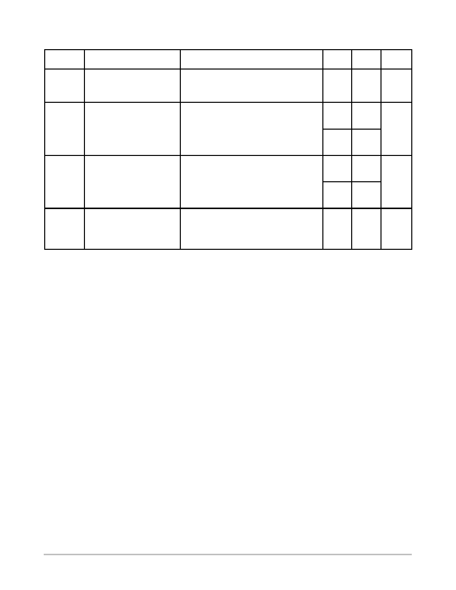
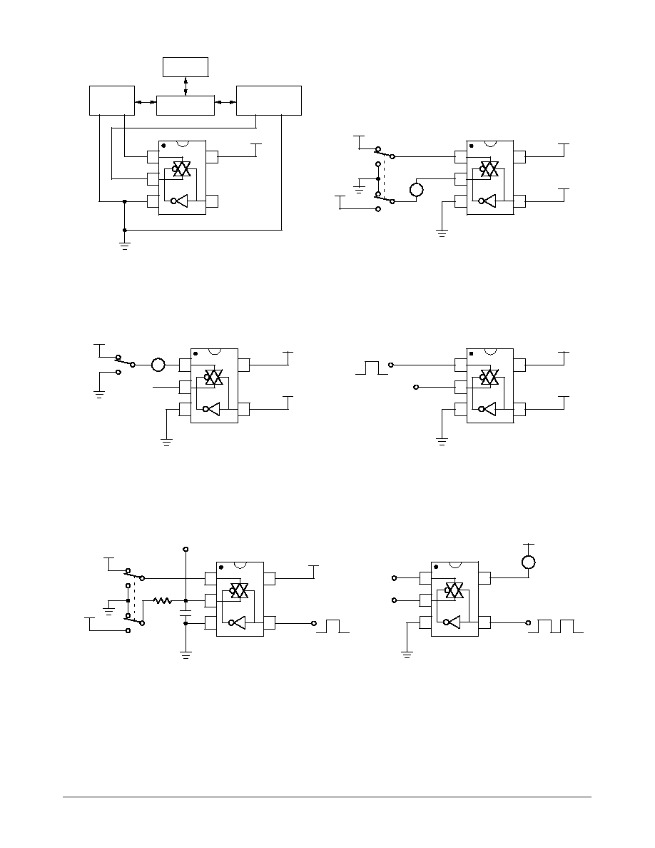
Figure 1. On Resistance Test Set≠Up
Figure 2. Maximum Off≠Channel Leakage Current
Test Set≠Up
5
1
2
4
3
Figure 3. Maximum On≠Channel Leakage Current
Test Set≠Up
Figure 4. Propagation Delay Test Set≠Up
Figure 5. Propagation Delay Output Enable/Disable
Test Set≠Up
Figure 6. Power Dissipation Capacitance Test
Set≠Up
POWER
SUPPLY
COMPUTER
DC PARAMETER
ANALYZER
VCC
+
≠
PLOTTER
5
1
2
4
3
VCC
VIL
VCC
VCC
A
5
1
2
4
3
VCC
VIH
VCC
A
N/C
5
1
2
4
3
VCC
VCC
TEST
POINT
5
1
2
4
3
VCC
VCC
VCC
2
1
2
1
RL
CL*
*Includes all probe and jig capacitance.
5
1
2
4
3
VCC
N/C
N/C
TEST POINT
Switch to Position 1 when testing tPLZ and tPZL
Switch to Position 2 when testing tPHZ and tPZH
A