 | –≠–ª–µ–∫—Ç—Ä–æ–Ω–Ω—ã–π –∫–æ–º–ø–æ–Ω–µ–Ω—Ç: MCR703A | –°–∫–∞—á–∞—Ç—å:  PDF PDF  ZIP ZIP |
©
Semiconductor Components Industries, LLC, 2000
May, 2000 ≠ Rev. 4
1
Publication Order Number:
MCR703A/D
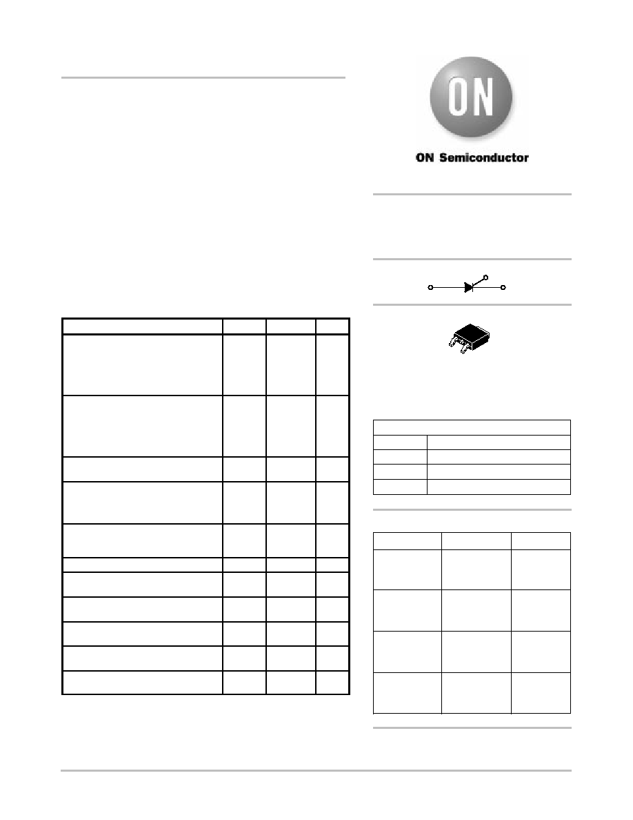
MCR703A Series
Preferred Device
Sensitive Gate
Silicon Controlled Rectifiers
Reverse Blocking Thyristors
PNPN devices designed for high volume, low cost consumer
applications such as temperature, light and speed control; process and
remote control; and warning systems where reliability of operation is
critical.
∑
Small Size
∑
Passivated Die Surface for Reliability and Uniformity
∑
Low Level Triggering and Holding Characteristics
∑
Recommend Electrical Replacement for C106
∑
Surface Mount Package -- Case 369A
∑
Device Marking: Device Type, e.g., for MCR703A: CR703A,
Date Code
MAXIMUM RATINGS
(TJ = 25
∞
C unless otherwise noted)
Rating
Symbol
Value
Unit
Peak Repetitive Off≠State Voltage(1)
(TC = ≠40 to +110
∞
C, Sine Wave,
50 to 60 Hz, Gate Open) MCR703A
MCR704A
MCR706A
MCR708A
VDRM,
VRRM
100
200
400
600
Volts
Peak Non-Repetitive Off≠State Voltage
(Sine Wave, 50 to 60 Hz, Gate Open,
TC = ≠40 to +110
∞
C)
MCR703A
MCR704A
MCR706A
MCR708A
VRSM
150
250
450
650
Volts
On≠State RMS Current
(180
∞
Conduction Angles, TC = 90
∞
C)
IT(RMS)
4.0
Amps
Average On≠State Current
(180
∞
Conduction Angles)
TC = ≠40 to +90
∞
C
TC = +100
∞
C
IT(AV)
2.6
1.6
Amps
Non-Repetitive Surge Current
(1/2 Sine Wave, 60 Hz, TJ = 110
∞
C)
(1/2 Sine Wave, 1.5 ms, TJ = 110
∞
C)
ITSM
25
35
Amps
Circuit Fusing (t = 8.3 ms)
I2t
2.6
A2s
Forward Peak Gate Power
(Pulse Width
10
m
s, TC = 90
∞
C)
PGM
0.5
Watt
Forward Average Gate Power
(t = 8.3 ms, TC = 90
∞
C)
PG(AV)
0.1
Watt
Forward Peak Gate Current
(Pulse Width
10
m
s, TC = 90
∞
C)
IGM
0.2
Amp
Operating Junction Temperature Range
TJ
≠ 40 to
+110
∞
C
Storage Temperature Range
Tstg
≠ 40 to
+150
∞
C
(1) VDRM and VRRM for all types can be applied on a continuous basis. Ratings
apply for zero or negative gate voltage; however, positive gate voltage shall
not be applied concurrent with negative potential on the anode. Blocking
voltages shall not be tested with a constant current source such that the
voltage ratings of the devices are exceeded.
SCRs
4.0 AMPERES RMS
100 thru 600 VOLTS
Device
Package
Shipping
ORDERING INFORMATION
MCR703AT4
DPAK 369A
16mm Tape
and Reel
(2.5K/Reel)
http://onsemi.com
K
G
A
MCR704AT4
DPAK 369A
16mm Tape
and Reel
(2.5K/Reel)
D≠PAK
CASE 369A
STYLE 5
1 2
3
4
PIN ASSIGNMENT
1
2
3
Anode
Cathode
Gate
4
Anode
Preferred devices are recommended choices for future use
and best overall value.
MCR706AT4
DPAK 369A
16mm Tape
and Reel
(2.5K/Reel)
MCR708AT4
DPAK 369A
16mm Tape
and Reel
(2.5K/Reel)
MCR703A Series
http://onsemi.com
2
THERMAL CHARACTERISTICS
Characteristic
Symbol
Max
Unit
Thermal Resistance, Junction to Case
R
JC
8.33
∞
C/W
Thermal Resistance, Junction to Ambient(1)
R
JA
80
∞
C/W
Maximum Lead Temperature for Soldering Purposes 1/8
from Case for 10 Seconds
TL
260
∞
C
ELECTRICAL CHARACTERISTICS
(TC = 25
∞
C unless otherwise noted.)
Characteristic
Symbol
Min
Typ
Max
Unit
OFF CHARACTERISTICS
Peak Repetitive Forward or Reverse Blocking Current
(VAK = Rated VDRM or VRRM; RGK = 1 K
)
TC = 25
∞
C
TC = 110
∞
C
IDRM, IRRM
--
--
--
--
10
200
µ
A
ON CHARACTERISTICS
Peak Forward "On" Voltage
(ITM = 8.2 A Peak, Pulse Width = 1 to 2 ms, 2% Duty Cycle)
VTM
--
--
2.2
Volts
Gate Trigger Current (Continuous dc)(2)
(VAK = 12 Vdc, RL = 24 Ohms)
TC = 25
∞
C
TC = ≠40
∞
C
IGT
--
--
25
--
75
300
µ
A
Gate Trigger Voltage (Continuous dc)(2)
TC = 25
∞
C
(VAK = 12 Vdc, RL = 24 Ohms)
TC = ≠40
∞
C
VGT
--
--
--
--
0.8
1.0
Volts
Gate Non-Trigger Voltage(2)
(VAK = 12 Vdc, RL = 100 Ohms, TC = 110
∞
C)
VGD
0.2
--
--
Volts
Holding Current
(VAK = 12 Vdc, Gate Open)
TC = 25
∞
C
(Initiating Current = 200 mA)
TC = ≠40
∞
C
IH
--
--
--
--
5.0
10
mA
Peak Reverse Gate Blocking Voltage
(IGR = 10
µ
A)
VRGM
10
12.5
18
Volts
Peak Reverse Gate Blocking Current
(VGR = 10 V)
IRGM
--
--
1.2
µ
A
Total Turn-On Time
(Source Voltage = 12 V, RS = 6 k Ohms)
(ITM = 8.2 A, IGT = 2 mA, Rated VDRM)
(Rise Time = 20 ns, Pulse Width = 10
µ
s)
tgt
--
2.0
--
µ
s
DYNAMIC CHARACTERISTICS
Critical Rate of Rise of Off≠State Voltage
(VD = Rated VDRM, RGK = 1 K
, Exponential Waveform,
TC = 110
∞
C)
dv/dt
--
10
--
V/
µ
s
Repetitive Critical Rate of Rise of On≠State Current
(Cf = 60 Hz, IPK = 30 A, PW = 100
µ
s, diG/dt = 1 A/
µ
s)
di/dt
--
--
100
A/
µ
s
(1) Case 369A when surface mounted on minimum pad sizes recommended.
(2) RGK current not included in measurement.

MCR703A Series
http://onsemi.com
3
+ Current
+ Voltage
VTM
IDRM at VDRM
IH
Symbol
Parameter
VDRM
Peak Repetitive Off State Forward Voltage
IDRM
Peak Forward Blocking Current
VRRM
Peak Repetitive Off State Reverse Voltage
IRRM
Peak Reverse Blocking Current
VTM
Peak On State Voltage
IH
Holding Current
Voltage Current Characteristic of SCR
Anode +
on state
Reverse Blocking Region
(off state)
Reverse Avalanche Region
Anode ≠
Forward Blocking Region
IRRM at VRRM
(off state)
30
∞
C
60
∞
C
90
∞
C
Figure 1. Average Current Derating
Figure 2. On≠State Power Dissipation
Figure 3. On≠State Characteristics
Figure 4. Transient Thermal Response
5.0
0
IT(AV), AVERAGE ON≠STATE CURRENT (AMPS)
110
105
IT(AV), AVERAGE ON≠STATE CURRENT (AMPS)
5.0
0
1.0
0
3.0
4.0
0.5
VT, INSTANTANEOUS ON≠STATE VOLTAGE (VOLTS)
100
10
1.0
0.1
t, TIME (ms)
1.0
0.1
1.0
0.1
0.01
3.5
T C
, MAXIMUM
ALLOW
ABLE CASE
TEMPERA
TURE ( C)
P
I
r (t)
, TRANSIENT
RESIST
ANCE
(NORMALIZED)
100
95
3.0
1.0
2.0
4.0
4.0
1.0
2.0
3.0
2.0
3.0
4.0
1.0
1.5
2.0
2.5
10
100
1000
10,000
∞
5.0
,
A
VERAGE POWER DISSIP
A
TION (W
A
TTS)
(A
V)
T
,
INST
ANT
ANEOUS ON≠ST
A
TE CURRENT
(AMPS)
4.5
ZqJC(t) = RqJC(t)
∑
r(t)
120
∞
C
180
∞
C
DC
30
∞
C
60
∞
C
90
∞
C
120
∞
C
180
∞
C
DC
Maximum @ TJ = 110
∞
C
Maximum @ TJ = 25
∞
C
Typical @ TJ = 25
∞
C

MCR703A Series
http://onsemi.com
4
110
≠40
TJ, JUNCTION TEMPERATURE (
∞
C)
2.0
1.5
I H
, HOLDING CURRENT
(mA)
I
0.5
0
20
≠20
0
40
, LA
TCHING
CURRENT
(mA)
L
1.0
60
80
100
110
≠40
TJ, JUNCTION TEMPERATURE (
∞
C)
2.0
1.5
0.5
0
20
≠20
0
40
1.0
60
80
100
TJ, JUNCTION TEMPERATURE (
∞
C)
1.0
0
0.5
V
GT
, GA
TE
TRIGGER
VOL
T
AGE
(VOL
TS)
≠20
40
≠40
0
20
100
60
80
110
Figure 5. Typical Gate Trigger Current versus
Junction Temperature
≠20
40
≠40
TJ, JUNCTION TEMPERATURE (
∞
C)
35
30
25
20
15
0
, GA
TE
TRIGGER
CURRENT
(
A)
I GT
20
100
60
80
110
m
Figure 6. Typical Gate Trigger Voltage versus
Junction Temperature
Figure 7. Typical Holding Current versus
Junction Temperature
Figure 8. Typical Latching Current versus
Junction Temperature

MCR703A Series
http://onsemi.com
5
MINIMUM RECOMMENDED FOOTPRINT FOR SURFACE MOUNTED APPLICATIONS
Surface mount board layout is a critical portion of the
total design. The footprint for the semiconductor packages
must be the correct size to insure proper solder connection
interface between the board and the package. With the
correct pad geometry, the packages will self align when
subjected to a solder reflow process.
DPAK
0.190
4.826
0.100
2.54
0.063
1.6
0.165
4.191
0.118
3.0
0.243
6.172
mm
inches