 | –≠–ª–µ–∫—Ç—Ä–æ–Ω–Ω—ã–π –∫–æ–º–ø–æ–Ω–µ–Ω—Ç: MJD117 | –°–∫–∞—á–∞—Ç—å:  PDF PDF  ZIP ZIP |
©
Semiconductor Components Industries, LLC, 2004
August, 2004 - Rev. 5
1
Publication Order Number:
MJD112/D
MJD112 (NPN)
MJD117 (PNP)
Preferred Device
Complementary Darlington
Power Transistors
DPAK For Surface Mount Applications
Designed for general purpose power and switching such as output or
driver stages in applications such as switching regulators, converters,
and power amplifiers.
Features
∑
Pb-Free Packages are Available
∑
Lead Formed for Surface Mount Applications in Plastic Sleeves
(No Suffix)
∑
Straight Lead Version in Plastic Sleeves ("-1" Suffix)
∑
Lead Formed Version in 16 mm Tape and Reel
("T4" and "RL" Suffix)
∑
Electrically Similar to Popular TIP31 and TIP32 Series
MAXIMUM RATINGS
Rating
Symbol
Max
Unit
Collector-Emitter Voltage
V
CEO
100
Vdc
Collector-Base Voltage
V
CB
100
Vdc
Emitter-Base Voltage
V
EB
5
Vdc
Collector Current - Continuous
Peak
I
C
2
4
Adc
Base Current
I
B
50
mAdc
Total Power Dissipation @ T
C
= 25
∞
C
Derate above 25
∞
C
P
D
20
0.16
W
W/
∞
C
Total Power Dissipation* @ T
A
= 25
∞
C
Derate above 25
∞
C
P
D
1.75
0.014
W
W/
∞
C
Operating and Storage Junction Temperature
Range
T
J
, T
stg
- 65 to
+ 150
∞
C
Maximum ratings are those values beyond which device damage can occur.
Maximum ratings applied to the device are individual stress limit values (not
normal operating conditions) and are not valid simultaneously. If these limits
are exceeded, device functional operation is not implied, damage may occur
and reliability may be affected.
THERMAL CHARACTERISTICS
Characteristic
Symbol
Max
Unit
Thermal Resistance, Junction-to-Case
R
q
JC
6.25
∞
C/W
Thermal Resistance, Junction-to-Ambient*
R
q
JA
71.4
∞
C/W
*These ratings are applicable when surface mounted on the minimum pad sizes
recommended.
SILICON
POWER TRANSISTORS
2 AMPERES
100 VOLTS
20 WATTS
DPAK-3
CASE 369D
DPAK
CASE 369C
MARKING
DIAGRAMS
Preferred devices are recommended choices for future use
and best overall value.
Y
= Year
WW
= Work Week
x
= 2 or 7
1 2
3
4
YWW
J11x
See detailed ordering and shipping information in the package
dimensions section on page 2 of this data sheet.
ORDERING INFORMATION
1
2
3
4
YWW
J11x
http://onsemi.com

MJD112 (NPN) MJD117 (PNP)
http://onsemi.com
2
ŒŒŒŒŒŒŒŒŒŒŒŒŒŒŒŒŒŒŒŒŒŒŒŒŒŒŒŒŒŒŒŒŒ
ŒŒŒŒŒŒŒŒŒŒŒŒŒŒŒŒŒŒŒŒŒŒŒŒŒŒŒŒŒŒŒŒŒ
ELECTRICAL CHARACTERISTICS
(T
C
= 25
_
C unless otherwise noted)
ŒŒŒŒŒŒŒŒŒŒŒŒŒŒŒŒŒŒŒŒŒŒŒ
ŒŒŒŒŒŒŒŒŒŒŒŒŒŒŒŒŒŒŒŒŒŒŒ
Characteristic
ŒŒŒŒ
ŒŒŒŒ
Symbol
ŒŒŒ
ŒŒŒ
Min
ŒŒŒŒ
ŒŒŒŒ
Max
ŒŒŒ
ŒŒŒ
Unit
ŒŒŒŒŒŒŒŒŒŒŒŒŒŒŒŒŒŒŒŒŒŒŒŒŒŒŒŒŒŒŒŒŒ
ŒŒŒŒŒŒŒŒŒŒŒŒŒŒŒŒŒŒŒŒŒŒŒŒŒŒŒŒŒŒŒŒŒ
OFF CHARACTERISTICS
ŒŒŒŒŒŒŒŒŒŒŒŒŒŒŒŒŒŒŒŒŒŒŒ
Œ
ŒŒŒŒŒŒŒŒŒŒŒŒŒŒŒŒŒŒŒŒŒ
Œ
ŒŒŒŒŒŒŒŒŒŒŒŒŒŒŒŒŒŒŒŒŒŒŒ
Collector-Emitter Sustaining Voltage (1)
(I
C
= 30 mAdc, I
B
= 0)
ŒŒŒŒ
Œ
ŒŒ
Œ
ŒŒŒŒ
V
CEO(sus)
ŒŒŒ
Œ
Œ
Œ
ŒŒŒ
100
ŒŒŒŒ
Œ
ŒŒ
Œ
ŒŒŒŒ
-
ŒŒŒ
Œ
Œ
Œ
ŒŒŒ
Vdc
ŒŒŒŒŒŒŒŒŒŒŒŒŒŒŒŒŒŒŒŒŒŒŒ
Œ
ŒŒŒŒŒŒŒŒŒŒŒŒŒŒŒŒŒŒŒŒŒ
Œ
ŒŒŒŒŒŒŒŒŒŒŒŒŒŒŒŒŒŒŒŒŒŒŒ
Collector Cutoff Current
(V
CE
= 50 Vdc, I
B
= 0)
ŒŒŒŒ
Œ
ŒŒ
Œ
ŒŒŒŒ
I
CEO
ŒŒŒ
Œ
Œ
Œ
ŒŒŒ
-
ŒŒŒŒ
Œ
ŒŒ
Œ
ŒŒŒŒ
20
ŒŒŒ
Œ
Œ
Œ
ŒŒŒ
m
Adc
ŒŒŒŒŒŒŒŒŒŒŒŒŒŒŒŒŒŒŒŒŒŒŒ
ŒŒŒŒŒŒŒŒŒŒŒŒŒŒŒŒŒŒŒŒŒŒŒ
Collector Cutoff Current
(V
CB
= 100 Vdc, I
E
= 0)
ŒŒŒŒ
ŒŒŒŒ
I
CBO
ŒŒŒ
ŒŒŒ
-
ŒŒŒŒ
ŒŒŒŒ
20
ŒŒŒ
ŒŒŒ
m
Adc
ŒŒŒŒŒŒŒŒŒŒŒŒŒŒŒŒŒŒŒŒŒŒŒ
Œ
ŒŒŒŒŒŒŒŒŒŒŒŒŒŒŒŒŒŒŒŒŒ
Œ
ŒŒŒŒŒŒŒŒŒŒŒŒŒŒŒŒŒŒŒŒŒŒŒ
Emitter Cutoff Current
(V
BE
= 5 Vdc, I
C
= 0)
ŒŒŒŒ
Œ
ŒŒ
Œ
ŒŒŒŒ
I
EBO
ŒŒŒ
Œ
Œ
Œ
ŒŒŒ
-
ŒŒŒŒ
Œ
ŒŒ
Œ
ŒŒŒŒ
2
ŒŒŒ
Œ
Œ
Œ
ŒŒŒ
mAdc
ŒŒŒŒŒŒŒŒŒŒŒŒŒŒŒŒŒŒŒŒŒŒŒ
ŒŒŒŒŒŒŒŒŒŒŒŒŒŒŒŒŒŒŒŒŒŒŒ
Collector-Cutoff Current (V
CB
= 80 Vdc, I
E
= 0)
ŒŒŒŒ
ŒŒŒŒ
I
CBO
ŒŒŒ
ŒŒŒ
-
ŒŒŒŒ
ŒŒŒŒ
10
ŒŒŒ
ŒŒŒ
m
Adc
ŒŒŒŒŒŒŒŒŒŒŒŒŒŒŒŒŒŒŒŒŒŒŒ
ŒŒŒŒŒŒŒŒŒŒŒŒŒŒŒŒŒŒŒŒŒŒŒ
Emitter-Cutoff Current (V
BE
= 5 Vdc, I
C
= 0)
ŒŒŒŒ
ŒŒŒŒ
I
EBO
ŒŒŒ
ŒŒŒ
-
ŒŒŒŒ
ŒŒŒŒ
2
ŒŒŒ
ŒŒŒ
mAdc
ŒŒŒŒŒŒŒŒŒŒŒŒŒŒŒŒŒŒŒŒŒŒŒŒŒŒŒŒŒŒŒŒŒ
ŒŒŒŒŒŒŒŒŒŒŒŒŒŒŒŒŒŒŒŒŒŒŒŒŒŒŒŒŒŒŒŒŒ
ON CHARACTERISTICS
ŒŒŒŒŒŒŒŒŒŒŒŒŒŒŒŒŒŒŒŒŒŒŒ
Œ
ŒŒŒŒŒŒŒŒŒŒŒŒŒŒŒŒŒŒŒŒŒ
Œ
Œ
ŒŒŒŒŒŒŒŒŒŒŒŒŒŒŒŒŒŒŒŒŒ
Œ
Œ
ŒŒŒŒŒŒŒŒŒŒŒŒŒŒŒŒŒŒŒŒŒ
Œ
ŒŒŒŒŒŒŒŒŒŒŒŒŒŒŒŒŒŒŒŒŒŒŒ
DC Current Gain
(I
C
= 0.5 Adc, V
CE
= 3 Vdc)
(I
C
= 2 Adc, V
CE
= 3 Vdc)
(I
C
= 4 Adc, V
CE
= 3 Vdc)
ŒŒŒŒ
Œ
ŒŒ
Œ
Œ
ŒŒ
Œ
Œ
ŒŒ
Œ
ŒŒŒŒ
h
FE
ŒŒŒ
Œ
Œ
Œ
Œ
Œ
Œ
Œ
Œ
Œ
ŒŒŒ
500
1000
200
ŒŒŒŒ
Œ
ŒŒ
Œ
Œ
ŒŒ
Œ
Œ
ŒŒ
Œ
ŒŒŒŒ
-
12,000
-
ŒŒŒ
Œ
Œ
Œ
Œ
Œ
Œ
Œ
Œ
Œ
ŒŒŒ
-
ŒŒŒŒŒŒŒŒŒŒŒŒŒŒŒŒŒŒŒŒŒŒŒ
Œ
ŒŒŒŒŒŒŒŒŒŒŒŒŒŒŒŒŒŒŒŒŒ
Œ
ŒŒŒŒŒŒŒŒŒŒŒŒŒŒŒŒŒŒŒŒŒŒŒ
Collector-Emitter Saturation Voltage
(I
C
= 2 Adc, I
B
= 8 mAdc)
(I
C
= 4 Adc, I
B
= 40 mAdc)
ŒŒŒŒ
Œ
ŒŒ
Œ
ŒŒŒŒ
V
CE(sat)
ŒŒŒ
Œ
Œ
Œ
ŒŒŒ
-
-
ŒŒŒŒ
Œ
ŒŒ
Œ
ŒŒŒŒ
2
3
ŒŒŒ
Œ
Œ
Œ
ŒŒŒ
Vdc
ŒŒŒŒŒŒŒŒŒŒŒŒŒŒŒŒŒŒŒŒŒŒŒ
ŒŒŒŒŒŒŒŒŒŒŒŒŒŒŒŒŒŒŒŒŒŒŒ
Base-Emitter Saturation Voltage (I
C
= 4 Adc, I
B
= 40 mAdc)
ŒŒŒŒ
ŒŒŒŒ
V
BE(sat)
ŒŒŒ
ŒŒŒ
-
ŒŒŒŒ
ŒŒŒŒ
4
ŒŒŒ
ŒŒŒ
Vdc
ŒŒŒŒŒŒŒŒŒŒŒŒŒŒŒŒŒŒŒŒŒŒŒ
ŒŒŒŒŒŒŒŒŒŒŒŒŒŒŒŒŒŒŒŒŒŒŒ
Base-Emitter On Voltage (I
C
= 2 Adc, V
CE
= 3 Vdc)
ŒŒŒŒ
ŒŒŒŒ
V
BE(on)
ŒŒŒ
ŒŒŒ
-
ŒŒŒŒ
ŒŒŒŒ
2.8
ŒŒŒ
ŒŒŒ
Vdc
ŒŒŒŒŒŒŒŒŒŒŒŒŒŒŒŒŒŒŒŒŒŒŒŒŒŒŒŒŒŒŒŒŒ
ŒŒŒŒŒŒŒŒŒŒŒŒŒŒŒŒŒŒŒŒŒŒŒŒŒŒŒŒŒŒŒŒŒ
DYNAMIC CHARACTERISTICS
ŒŒŒŒŒŒŒŒŒŒŒŒŒŒŒŒŒŒŒŒŒŒŒ
Œ
ŒŒŒŒŒŒŒŒŒŒŒŒŒŒŒŒŒŒŒŒŒ
Œ
ŒŒŒŒŒŒŒŒŒŒŒŒŒŒŒŒŒŒŒŒŒŒŒ
Current-Gain - Bandwidth Product
(I
C
= 0.75 Adc, V
CE
= 10 Vdc, f = 1 MHz)
ŒŒŒŒ
Œ
ŒŒ
Œ
ŒŒŒŒ
f
T
ŒŒŒ
Œ
Œ
Œ
ŒŒŒ
25
ŒŒŒŒ
Œ
ŒŒ
Œ
ŒŒŒŒ
-
ŒŒŒ
Œ
Œ
Œ
ŒŒŒ
MHz
ŒŒŒŒŒŒŒŒŒŒŒŒŒŒŒŒŒŒŒŒŒŒŒ
Œ
ŒŒŒŒŒŒŒŒŒŒŒŒŒŒŒŒŒŒŒŒŒ
Œ
Œ
ŒŒŒŒŒŒŒŒŒŒŒŒŒŒŒŒŒŒŒŒŒ
Œ
ŒŒŒŒŒŒŒŒŒŒŒŒŒŒŒŒŒŒŒŒŒŒŒ
Output Capacitance
(V
CB
= 10 Vdc, I
E
= 0, f = 0.1 MHz)
MJD117
MJD112
ŒŒŒŒ
Œ
ŒŒ
Œ
Œ
ŒŒ
Œ
ŒŒŒŒ
C
ob
ŒŒŒ
Œ
Œ
Œ
Œ
Œ
Œ
ŒŒŒ
-
-
ŒŒŒŒ
Œ
ŒŒ
Œ
Œ
ŒŒ
Œ
ŒŒŒŒ
200
100
ŒŒŒ
Œ
Œ
Œ
Œ
Œ
Œ
ŒŒŒ
pF
1. Pulse Test: Pulse Width
v
300
m
s, Duty Cycle
v
2%.
*These ratings are applicable when surface mounted on the minimum pad sizes recommended.
ORDERING INFORMATION
Device
Package Type
Package
Shipping
MJD112
DPAK
369C
75 Units / Rail
MJD112-001
DPAK-3
369D
75 Units / Rail
MJD112RL
DPAK
369C
1800 Tape & Reel
MJD112T4
DPAK
369C
2500 Tape & Reel
MJD112T4G
DPAK
(Pb-Free)
369C
2500 Tape & Reel
MJD117
DPAK
369C
75 Units / Rail
MJD117G
DPAK
(Pb-Free)
369C
75 Units / Rail
MJD117-001
DPAK-3
369D
75 Units / Rail
MJD117T4
DPAK
369C
2500 Tape & Reel
For information on tape and reel specifications, including part orientation and tape sizes, please refer to our Tape and Reel Packaging
Specifications Brochure, BRD8011/D.
MJD112 (NPN) MJD117 (PNP)
http://onsemi.com
3
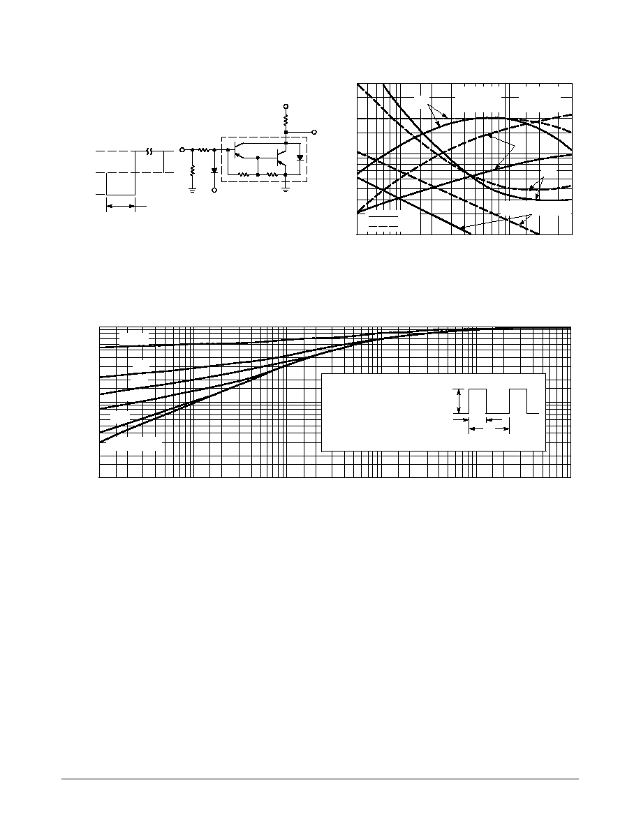
0.04
0.2
4
0.1
0.06
0.6
1
4
I
C
, COLLECTOR CURRENT (AMP)
V
CC
= 30 V
I
C
/I
B
= 250
t, TIME
(s)
µ
2
1
0.8
0.6
0.4
0.2
t
s
t
f
Figure 1. Switching Times Test Circuit
Figure 2. Switching Times
V
2
APPROX
+8 V
0
8 k
SCOPE
V
CC
-30 V
R
C
51
FOR t
d
AND t
r
, D
1
IS DISCONNECTED
AND V
2
= 0
FOR NPN TEST CIRCUIT REVERSE ALL POLARITIES.
25
ms
t
r
, t
f
10 ns
DUTY CYCLE = 1%
+ 4 V
t
r
t
d
@ V
BE(off)
= 0 V
PNP
NPN
R
B
& R
C
VARIED TO OBTAIN DESIRED CURRENT LEVELS
D
1
, MUST BE FAST RECOVERY TYPE, e.g.:
1N5825 USED ABOVE I
B
100 mA
MSD6100 USED BELOW I
B
100 mA
V
1
APPROX
-12 V
TUT
R
B
D
1
60
0.4
2
I
B1
= I
B2
T
J
= 25
∞
C
Figure 3. Thermal Response
t, TIME OR PULSE WIDTH (ms)
1
0.01
1000
0.3
0.2
0.07
r(t)
, EFFECTIVE
TRANSIENT
R
qJC(t)
= r(t) R
qJC
R
qJC
= 6.25
∞
C/W
D CURVES APPLY FOR POWER
PULSE TRAIN SHOWN
READ TIME AT t
1
T
J(pk)
- T
C
= P
(pk)
q
JC(t)
P
(pk)
t
1
t
2
DUTY CYCLE, D = t
1
/t
2
0.01
THERMAL
RESIST
ANCE (NORMALIZED)
0.7
0.5
0.1
0.05
0.03
0.02
0.02 0.03
0.05
0.1
0.2 0.3
0.5
1
2
3
5
10
20
30
50
100
200 300
500
0.2
SINGLE PULSE
D = 0.5
0.05
0.1
0.01
MJD112 (NPN) MJD117 (PNP)
http://onsemi.com
4
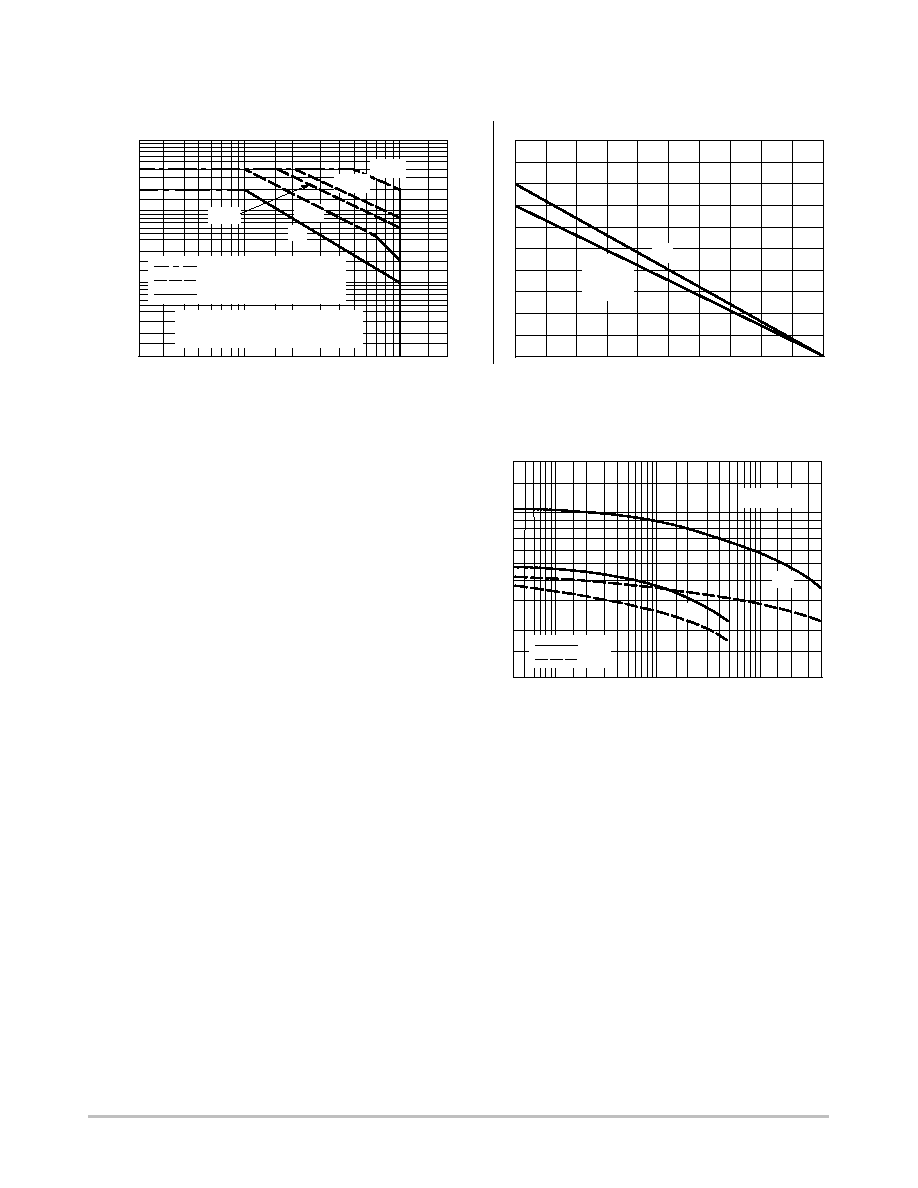
I C
, COLLECT
OR CURRENT
(AMP)
Figure 4. Maximum Rated Forward Biased
Safe Operating Area
Figure 5. Power Derating
2
V
CE
, COLLECTOR-EMITTER VOLTAGE (VOLTS)
0.3
100
5
2
0.5
0.2
BONDING WIRE LIMITED
THERMAL LIMIT
SECOND BREAKDOWN LIMIT
5
20
3
T
J
= 150
∞
C
CURVES APPLY BELOW RATED V
CEO
100
ms
1 ms
dc
0.1
1
3
7
10
10
7
30
25
25
T, TEMPERATURE (
∞
C)
0
50
75
100
125
15
20
15
10
5
P
D
, POWER DISSIP
A
TION (W
A
TTS)
2.5
0
2
1.5
1
0.5
T
A
T
C
T
A
SURFACE
MOUNT
T
C
0.7
5 ms
50
70
200
500
ms
ACTIVE-REGION SAFE-OPERATING AREA
There are two limitations on the power handling ability of
a transistor: average junction temperature and second
breakdown. Safe operating area curves indicate I
C
- V
CE
limits of the transistor that must be observed for reliable
operation; i.e., the transistor must not be subjected to greater
dissipation than the curves indicate.
The data of Figures 5 and 6 is based on T
J(pk)
= 150
_C;
T
C
is variable depending on conditions. Second breakdown
pulse limits are valid for duty cycles to 10% provided T
J(pk)
< 150
_C. T
J(pk)
may be calculated from the data in
Figure 4. At high case temperatures, thermal limitations will
reduce the power that can be handled to values less than the
limitations imposed by second breakdown.
C, CAP
ACIT
ANCE (pF)
V
R
, REVERSE VOLTAGE (VOLTS)
C
ib
0.04
30
1
4
10
40
T
C
= 25
∞
C
200
10
50
70
100
0.1
2
6
20
20
PNP
NPN
0.6
0.4
0.2
0.06
Figure 6. Capacitance
C
ob
MJD112 (NPN) MJD117 (PNP)
http://onsemi.com
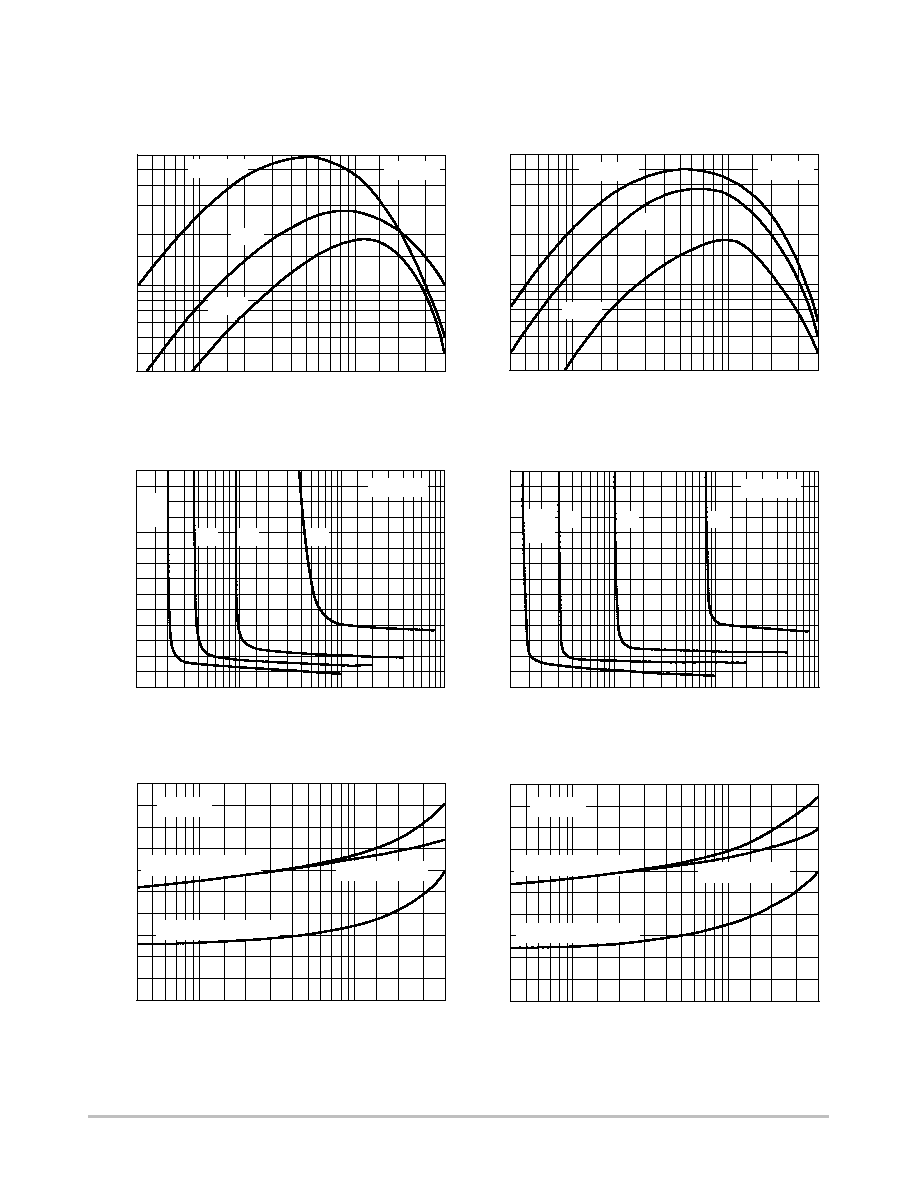
5
V
CE
, COLLECT
OR-EMITTER VOL
T
AGE (VOL
TS)
V
CE
, COLLECT
OR-EMITTER VOL
T
AGE (VOL
TS)
I
C
, COLLECTOR CURRENT (AMP)
NPN MJD112
PNP MJD117
Figure 7. DC Current Gain
Figure 8. Collector Saturation Region
Figure 9. "On Voltages
0.04
I
C
, COLLECTOR CURRENT (AMP)
300
0.06
0.2
2 k
800
4 k
h
FE
, DC CURRENT
GAIN
V
CE
= 3 V
T
J
= 125
∞
C
3 k
0.1
0.6
25
∞
C
-55
∞
C
1 k
0.4
1
6 k
400
600
2
4
0.04
300
0.06
0.2
2 k
800
4 k
h
FE
, DC CURRENT
GAIN
3 k
0.1
0.6
25
∞
C
-55
∞
C
1 k
0.4
1
6 k
400
600
2
4
3.4
I
B
, BASE CURRENT (mA)
2.6
2.2
1.8
1.4
0.6
0.1
0.2
0.5
10
2
5
I
C
=
0.5 A
1 A
1
3
1
0.04
I
C
, COLLECTOR CURRENT (AMP)
1.4
1
V
,
VOL
T
AGE (VOL
TS)
2.2
1.8
0.6
0.2
T
J
= 25
∞
C
V
BE(sat)
@ I
C
/I
B
= 250
V
BE
@ V
CE
= 3 V
V
CE(sat)
@ I
C
/I
B
= 250
0.06
0.2
2
0.1
0.6
0.4
1
4
0.04
I
C
, COLLECTOR CURRENT (AMP)
1.4
1
V
,
VOL
T
AGE (VOL
TS)
2.2
1.8
0.6
0.2
T
J
= 25
∞
C
V
BE(sat)
@ I
C
/I
B
= 250
V
CE(sat)
@ I
C
/I
B
= 250
0.06
0.2
2
0.1
0.6
0.4
1
4
20
50
100
3.4
I
B
, BASE CURRENT (mA)
2.6
2.2
1.8
1.4
0.6
0.1
0.2
0.5
10
2
5
1
3
1
20
50
100
V
BE
@ V
CE
= 3 V
T
C
= 125
∞
C
V
CE
= 3 V
4 A
T
J
= 125
∞
C
2 A
T
J
= 125
∞
C
I
C
=
0.5 A
1 A
4 A
2 A
TYPICAL ELECTRICAL CHARACTERISTICS