 | –≠–ª–µ–∫—Ç—Ä–æ–Ω–Ω—ã–π –∫–æ–º–ø–æ–Ω–µ–Ω—Ç: MJD31 | –°–∫–∞—á–∞—Ç—å:  PDF PDF  ZIP ZIP |

©
Semiconductor Components Industries, LLC, 2001
November, 2001 ≠ Rev. 3
1
Publication Order Number:
MJD31/D
MJD31, MJD31C (NPN),
MJD32, MJD32C (PNP)
MJD31C and MJD32C are Preferred Devices
Complementary Power
Transistors
DPAK For Surface Mount Applications
Designed for general purpose amplifier and low speed switching
applications.
∑
Lead Formed for Surface Mount Applications in Plastic Sleeves
(No Suffix)
∑
Straight Lead Version in Plastic Sleeves ("≠1" Suffix)
∑
Lead Formed Version in 16 mm Tape and Reel ("T4" Suffix)
∑
Electrically Similar to Popular TIP31 and TIP32 Series
ŒŒŒŒŒŒŒŒŒŒŒŒŒŒŒŒŒŒŒ
ŒŒŒŒŒŒŒŒŒŒŒŒŒŒŒŒŒŒŒ
MAXIMUM RATINGS
ŒŒŒŒŒŒŒŒŒŒ
Œ
ŒŒŒŒŒŒŒŒ
Œ
ŒŒŒŒŒŒŒŒŒŒ
Rating
ŒŒŒ
Œ
Œ
Œ
ŒŒŒ
Symbol
ŒŒŒŒ
Œ
ŒŒ
Œ
ŒŒŒŒ
MJD31
MJD32
ŒŒŒŒ
Œ
ŒŒ
Œ
ŒŒŒŒ
MJD31C
MJD32C
ŒŒ
ŒŒ
ŒŒ
Unit
ŒŒŒŒŒŒŒŒŒŒ
ŒŒŒŒŒŒŒŒŒŒ
Collector≠Emitter Voltage
ŒŒŒ
ŒŒŒ
V
CEO
ŒŒŒŒ
ŒŒŒŒ
40
ŒŒŒŒ
ŒŒŒŒ
100
ŒŒ
ŒŒ
Vdc
ŒŒŒŒŒŒŒŒŒŒ
ŒŒŒŒŒŒŒŒŒŒ
Collector≠Base Voltage
ŒŒŒ
ŒŒŒ
V
CB
ŒŒŒŒ
ŒŒŒŒ
40
ŒŒŒŒ
ŒŒŒŒ
100
ŒŒ
ŒŒ
Vdc
ŒŒŒŒŒŒŒŒŒŒ
ŒŒŒŒŒŒŒŒŒŒ
Emitter≠Base Voltage
ŒŒŒ
ŒŒŒ
V
EB
ŒŒŒŒŒŒŒ
ŒŒŒŒŒŒŒ
5
ŒŒ
ŒŒ
Vdc
ŒŒŒŒŒŒŒŒŒŒ
Œ
ŒŒŒŒŒŒŒŒ
Œ
ŒŒŒŒŒŒŒŒŒŒ
Collector Current ≠ Continuous
Peak
ŒŒŒ
Œ
Œ
Œ
ŒŒŒ
I
C
ŒŒŒŒŒŒŒ
Œ
ŒŒŒŒŒ
Œ
ŒŒŒŒŒŒŒ
3
5
ŒŒ
ŒŒ
ŒŒ
Adc
ŒŒŒŒŒŒŒŒŒŒ
ŒŒŒŒŒŒŒŒŒŒ
Base Current
ŒŒŒ
ŒŒŒ
I
B
ŒŒŒŒŒŒŒ
ŒŒŒŒŒŒŒ
1
ŒŒ
ŒŒ
Adc
ŒŒŒŒŒŒŒŒŒŒ
Œ
ŒŒŒŒŒŒŒŒ
Œ
ŒŒŒŒŒŒŒŒŒŒ
Total Power Dissipation
@ T
C
= 25
_
C
Derate above 25
_
C
ŒŒŒ
Œ
Œ
Œ
ŒŒŒ
P
D
ŒŒŒŒŒŒŒ
Œ
ŒŒŒŒŒ
Œ
ŒŒŒŒŒŒŒ
15
0.12
ŒŒ
ŒŒ
ŒŒ
Watts
W/
_
C
ŒŒŒŒŒŒŒŒŒŒ
Œ
ŒŒŒŒŒŒŒŒ
Œ
Œ
ŒŒŒŒŒŒŒŒ
Œ
ŒŒŒŒŒŒŒŒŒŒ
Total Power Dissipation (Note 1)
@ T
A
= 25
_
C
Derate above 25
_
C
ŒŒŒ
Œ
Œ
Œ
Œ
Œ
Œ
ŒŒŒ
P
D
ŒŒŒŒŒŒŒ
Œ
ŒŒŒŒŒ
Œ
Œ
ŒŒŒŒŒ
Œ
ŒŒŒŒŒŒŒ
1.56
0.012
ŒŒ
ŒŒ
ŒŒ
ŒŒ
Watts
W/
_
C
ŒŒŒŒŒŒŒŒŒŒ
ŒŒŒŒŒŒŒŒŒŒ
Operating and Storage Junction
Temperature Range
ŒŒŒ
ŒŒŒ
T
J
, T
stg
ŒŒŒŒŒŒŒ
ŒŒŒŒŒŒŒ
≠65 to +150
ŒŒ
ŒŒ
_
C
1. These ratings are applicable when surface mounted on the minimum pad size
recommended.
http://onsemi.com
MARKING
DIAGRAMS
DPAK
CASE 369A
STYLE 1
SILICON
POWER TRANSISTORS
3 AMPERES
40 AND 100 VOLTS
15 WATTS
DPAK
STRAIGHT LEADS
CASE 369
STYLE 1
Preferred devices are recommended choices for future use
and best overall value.
MJD3xx
YWW
MJD3xx = Specific Device Code
xx
= 1, 1C, 2 or 2C
Y
= Year
WW
= Work Week
See detailed ordering and shipping information in the package
dimensions section on page 5 of this data sheet.
ORDERING INFORMATION
1
4
1
4
MJD3xx
YWW

MJD31, MJD31C (NPN), MJD32, MJD32C (PNP)
http://onsemi.com
2
ŒŒŒŒŒŒŒŒŒŒŒŒŒŒŒŒŒŒŒŒŒŒŒŒŒŒŒŒŒŒŒŒŒ
ŒŒŒŒŒŒŒŒŒŒŒŒŒŒŒŒŒŒŒŒŒŒŒŒŒŒŒŒŒŒŒŒŒ
THERMAL CHARACTERISTICS
ŒŒŒŒŒŒŒŒŒŒŒŒŒŒŒŒŒŒ
ŒŒŒŒŒŒŒŒŒŒŒŒŒŒŒŒŒŒ
Characteristic
ŒŒŒŒŒ
ŒŒŒŒŒ
Symbol
ŒŒŒŒŒŒŒŒŒ
ŒŒŒŒŒŒŒŒŒ
Max
ŒŒŒŒ
ŒŒŒŒ
Unit
ŒŒŒŒŒŒŒŒŒŒŒŒŒŒŒŒŒŒ
ŒŒŒŒŒŒŒŒŒŒŒŒŒŒŒŒŒŒ
Thermal Resistance, Junction to Case
ŒŒŒŒŒ
ŒŒŒŒŒ
R
JC
ŒŒŒŒŒŒŒŒŒ
ŒŒŒŒŒŒŒŒŒ
8.3
ŒŒŒŒ
ŒŒŒŒ
_
C/W
ŒŒŒŒŒŒŒŒŒŒŒŒŒŒŒŒŒŒ
ŒŒŒŒŒŒŒŒŒŒŒŒŒŒŒŒŒŒ
Thermal Resistance, Junction to Ambient (Note 2)
ŒŒŒŒŒ
ŒŒŒŒŒ
R
JA
ŒŒŒŒŒŒŒŒŒ
ŒŒŒŒŒŒŒŒŒ
80
ŒŒŒŒ
ŒŒŒŒ
_
C/W
ŒŒŒŒŒŒŒŒŒŒŒŒŒŒŒŒŒŒ
ŒŒŒŒŒŒŒŒŒŒŒŒŒŒŒŒŒŒ
Lead Temperature for Soldering Purposes
ŒŒŒŒŒ
ŒŒŒŒŒ
T
L
ŒŒŒŒŒŒŒŒŒ
ŒŒŒŒŒŒŒŒŒ
260
ŒŒŒŒ
ŒŒŒŒ
_
C
2. These ratings are applicable when surface mounted on the minimum pad size recommended.
ŒŒŒŒŒŒŒŒŒŒŒŒŒŒŒŒŒŒŒŒŒŒŒŒŒŒŒŒŒŒŒŒŒ
ŒŒŒŒŒŒŒŒŒŒŒŒŒŒŒŒŒŒŒŒŒŒŒŒŒŒŒŒŒŒŒŒŒ
ELECTRICAL CHARACTERISTICS
(T
C
= 25
_
C unless otherwise noted)
ŒŒŒŒŒŒŒŒŒŒŒŒŒŒŒŒŒŒ
ŒŒŒŒŒŒŒŒŒŒŒŒŒŒŒŒŒŒ
Characteristic
ŒŒŒŒŒ
ŒŒŒŒŒ
Symbol
ŒŒŒŒŒ
ŒŒŒŒŒ
Min
ŒŒŒŒŒ
ŒŒŒŒŒ
Max
ŒŒŒŒ
ŒŒŒŒ
Unit
ŒŒŒŒŒŒŒŒŒŒŒŒŒŒŒŒŒŒŒŒŒŒŒŒŒŒŒŒŒŒŒŒŒ
ŒŒŒŒŒŒŒŒŒŒŒŒŒŒŒŒŒŒŒŒŒŒŒŒŒŒŒŒŒŒŒŒŒ
OFF CHARACTERISTICS
ŒŒŒŒŒŒŒŒŒŒŒŒŒŒŒŒŒŒ
Œ
ŒŒŒŒŒŒŒŒŒŒŒŒŒŒŒŒ
Œ
Œ
ŒŒŒŒŒŒŒŒŒŒŒŒŒŒŒŒ
Œ
ŒŒŒŒŒŒŒŒŒŒŒŒŒŒŒŒŒŒ
Collector≠Emitter Sustaining Voltage (Note 3)
(I
C
= 30 mAdc, I
B
= 0)
MJD31, MJD32
MJD31C, MJD32C
ŒŒŒŒŒ
Œ
ŒŒŒ
Œ
Œ
ŒŒŒ
Œ
ŒŒŒŒŒ
V
CEO(sus)
ŒŒŒŒŒ
Œ
ŒŒŒ
Œ
Œ
ŒŒŒ
Œ
ŒŒŒŒŒ
40
100
ŒŒŒŒŒ
Œ
ŒŒŒ
Œ
Œ
ŒŒŒ
Œ
ŒŒŒŒŒ
≠
≠
ŒŒŒŒ
Œ
ŒŒ
Œ
Œ
ŒŒ
Œ
ŒŒŒŒ
Vdc
ŒŒŒŒŒŒŒŒŒŒŒŒŒŒŒŒŒŒ
Œ
ŒŒŒŒŒŒŒŒŒŒŒŒŒŒŒŒ
Œ
ŒŒŒŒŒŒŒŒŒŒŒŒŒŒŒŒŒŒ
Collector Cutoff Current
(V
CE
= 40 Vdc, I
B
= 0)
MJD31, MJD32
(V
CE
= 60 Vdc, I
B
= 0)
MJD31C, MJD32C
ŒŒŒŒŒ
Œ
ŒŒŒ
Œ
ŒŒŒŒŒ
I
CEO
ŒŒŒŒŒ
Œ
ŒŒŒ
Œ
ŒŒŒŒŒ
≠
ŒŒŒŒŒ
Œ
ŒŒŒ
Œ
ŒŒŒŒŒ
50
ŒŒŒŒ
Œ
ŒŒ
Œ
ŒŒŒŒ
µ
Adc
ŒŒŒŒŒŒŒŒŒŒŒŒŒŒŒŒŒŒ
Œ
ŒŒŒŒŒŒŒŒŒŒŒŒŒŒŒŒ
Œ
ŒŒŒŒŒŒŒŒŒŒŒŒŒŒŒŒŒŒ
Collector Cutoff Current
(V
CE
= Rated V
CEO
, V
EB
= 0)
ŒŒŒŒŒ
Œ
ŒŒŒ
Œ
ŒŒŒŒŒ
ICES
ŒŒŒŒŒ
Œ
ŒŒŒ
Œ
ŒŒŒŒŒ
≠
ŒŒŒŒŒ
Œ
ŒŒŒ
Œ
ŒŒŒŒŒ
20
ŒŒŒŒ
Œ
ŒŒ
Œ
ŒŒŒŒ
µ
Adc
ŒŒŒŒŒŒŒŒŒŒŒŒŒŒŒŒŒŒ
Œ
ŒŒŒŒŒŒŒŒŒŒŒŒŒŒŒŒ
Œ
ŒŒŒŒŒŒŒŒŒŒŒŒŒŒŒŒŒŒ
Emitter Cutoff Current
(V
BE
= 5 Vdc, I
C
= 0)
ŒŒŒŒŒ
Œ
ŒŒŒ
Œ
ŒŒŒŒŒ
I
EBO
ŒŒŒŒŒ
Œ
ŒŒŒ
Œ
ŒŒŒŒŒ
≠
ŒŒŒŒŒ
Œ
ŒŒŒ
Œ
ŒŒŒŒŒ
1
ŒŒŒŒ
Œ
ŒŒ
Œ
ŒŒŒŒ
mAdc
ŒŒŒŒŒŒŒŒŒŒŒŒŒŒŒŒŒŒŒŒŒŒŒŒŒŒŒŒŒŒŒŒŒ
ŒŒŒŒŒŒŒŒŒŒŒŒŒŒŒŒŒŒŒŒŒŒŒŒŒŒŒŒŒŒŒŒŒ
ON CHARACTERISTICS (Note 3)
ŒŒŒŒŒŒŒŒŒŒŒŒŒŒŒŒŒŒ
Œ
ŒŒŒŒŒŒŒŒŒŒŒŒŒŒŒŒ
Œ
Œ
ŒŒŒŒŒŒŒŒŒŒŒŒŒŒŒŒ
Œ
ŒŒŒŒŒŒŒŒŒŒŒŒŒŒŒŒŒŒ
DC Current Gain
(I
C
= 1 Adc, V
CE
= 4 Vdc)
(I
C
= 3 Adc, V
CE
= 4 Vdc)
ŒŒŒŒŒ
Œ
ŒŒŒ
Œ
Œ
ŒŒŒ
Œ
ŒŒŒŒŒ
h
FE
ŒŒŒŒŒ
Œ
ŒŒŒ
Œ
Œ
ŒŒŒ
Œ
ŒŒŒŒŒ
25
10
ŒŒŒŒŒ
Œ
ŒŒŒ
Œ
Œ
ŒŒŒ
Œ
ŒŒŒŒŒ
≠
50
ŒŒŒŒ
Œ
ŒŒ
Œ
Œ
ŒŒ
Œ
ŒŒŒŒ
≠
ŒŒŒŒŒŒŒŒŒŒŒŒŒŒŒŒŒŒ
Œ
ŒŒŒŒŒŒŒŒŒŒŒŒŒŒŒŒ
Œ
ŒŒŒŒŒŒŒŒŒŒŒŒŒŒŒŒŒŒ
Collector≠Emitter Saturation Voltage
(I
C
= 3 Adc, I
B
= 375 mAdc)
ŒŒŒŒŒ
Œ
ŒŒŒ
Œ
ŒŒŒŒŒ
V
CE(sat)
ŒŒŒŒŒ
Œ
ŒŒŒ
Œ
ŒŒŒŒŒ
≠
ŒŒŒŒŒ
Œ
ŒŒŒ
Œ
ŒŒŒŒŒ
1.2
ŒŒŒŒ
Œ
ŒŒ
Œ
ŒŒŒŒ
Vdc
ŒŒŒŒŒŒŒŒŒŒŒŒŒŒŒŒŒŒ
Œ
ŒŒŒŒŒŒŒŒŒŒŒŒŒŒŒŒ
Œ
Base≠Emitter On Voltage
(I
C
= 3 Adc, V
CE
= 4 Vdc)
ŒŒŒŒŒ
Œ
ŒŒŒ
Œ
V
BE(on)
ŒŒŒŒŒ
Œ
ŒŒŒ
Œ
≠
ŒŒŒŒŒ
Œ
ŒŒŒ
Œ
1.8
ŒŒŒŒ
Œ
ŒŒ
Œ
Vdc
ŒŒŒŒŒŒŒŒŒŒŒŒŒŒŒŒŒŒŒŒŒŒŒŒŒŒŒŒŒŒŒŒŒ
Œ
ŒŒŒŒŒŒŒŒŒŒŒŒŒŒŒŒŒŒŒŒŒŒŒŒŒŒŒŒŒŒŒ
Œ
DYNAMIC CHARACTERISTICS
ŒŒŒŒŒŒŒŒŒŒŒŒŒŒŒŒŒŒ
Œ
ŒŒŒŒŒŒŒŒŒŒŒŒŒŒŒŒ
Œ
ŒŒŒŒŒŒŒŒŒŒŒŒŒŒŒŒŒŒ
Current Gain ≠ Bandwidth Product (Note 4)
(I
C
= 500 mAdc, V
CE
= 10 Vdc, f
test
= 1 MHz)
ŒŒŒŒŒ
Œ
ŒŒŒ
Œ
ŒŒŒŒŒ
f
T
ŒŒŒŒŒ
Œ
ŒŒŒ
Œ
ŒŒŒŒŒ
3
ŒŒŒŒŒ
Œ
ŒŒŒ
Œ
ŒŒŒŒŒ
≠
ŒŒŒŒ
Œ
ŒŒ
Œ
ŒŒŒŒ
MHz
ŒŒŒŒŒŒŒŒŒŒŒŒŒŒŒŒŒŒ
Œ
ŒŒŒŒŒŒŒŒŒŒŒŒŒŒŒŒ
Œ
ŒŒŒŒŒŒŒŒŒŒŒŒŒŒŒŒŒŒ
Small≠Signal Current Gain
(I
C
= 0.5 Adc, V
CE
= 10 Vdc, f = 1 kHz)
ŒŒŒŒŒ
Œ
ŒŒŒ
Œ
ŒŒŒŒŒ
h
fe
ŒŒŒŒŒ
Œ
ŒŒŒ
Œ
ŒŒŒŒŒ
20
ŒŒŒŒŒ
Œ
ŒŒŒ
Œ
ŒŒŒŒŒ
≠
ŒŒŒŒ
Œ
ŒŒ
Œ
ŒŒŒŒ
≠
3. Pulse Test: Pulse Width
v
300
µ
s, Duty Cycle
v
2%.
4. f
T
=
h
fe
∑
f
test
.

MJD31, MJD31C (NPN), MJD32, MJD32C (PNP)
http://onsemi.com
3
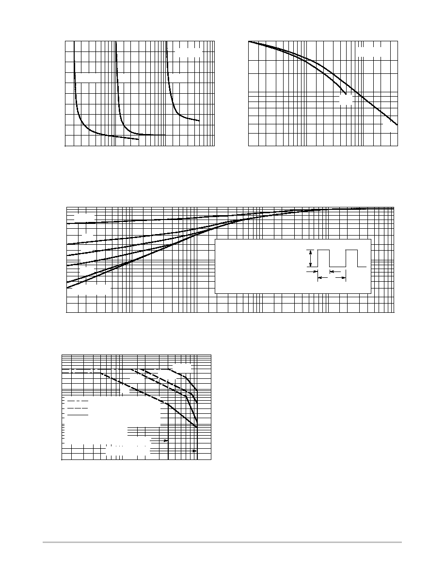
0.03
I
C
, COLLECTOR CURRENT (AMPS)
5
0.07
0.3
3
70
30
300
h FE
, DC CURRENT
GAIN
V
CE
= 2 V
T
J
= 150
∞
C
100
0.1
0.7
25
∞
C
-55
∞
C
50
0.05
0.5
1
25
25
Figure 1. Power Derating
T, TEMPERATURE (
∞
C)
0
50
75
100
125
150
20
15
10
5
P D
, POWER DISSIP
A
TION (W
A
TTS)
Figure 2. Switching Time Test Circuit
Figure 3. DC Current Gain
3
0.03
I
C
, COLLECTOR CURRENT (AMPS)
0.03
0.05 0.07 0.1
0.2
0.5 0.7
3
I
B1
= I
B2
I
C
/I
B
= 10
t
s
= t
s
- 1/8 t
f
T
J
= 25
∞
C
t, TIME
(s)
µ
0.3
2
1
0.7
0.5
0.3
t
s
0.2
0.1
0.07
0.05
1
2
Figure 4. Turn≠On Time
2
I
C
, COLLECTOR CURRENT (AMPS)
0.02
I
C
/I
B
= 10
T
J
= 25
∞
C
t, TIME
(s)
µ
1
0.7
0.5
0.3
0.1
0.07
0.05
0.03
0.003
Figure 5. "On" Voltages
I
C
, COLLECTOR CURRENT (AMPS)
1
0.8
V
,
VOL
T
AGE (VOL
TS)
1.4
1.2
0.4
0
+11 V
25
µ
s
0
-9 V
R
B
-4 V
D
1
SCOPE
V
CC
+30 V
R
C
t
r
, t
f
10 ns
DUTY CYCLE = 1%
51
R
B
and R
C
VARIED TO OBTAIN DESIRED CURRENT LEVELS
D
1
MUST BE FAST RECOVERY TYPE, e.g.:
1N5825 USED ABOVE I
B
100 mA
MSD6100 USED BELOW I
B
100 mA
REVERSE ALL POLARITIES FOR PNP.
500
7
10
0.03
0.07
0.3
3
0.1
0.7
0.05
0.5
1
t
r
@ V
CC
= 30 V
t
r
@ V
CC
= 10 V
t
d
@ V
BE(off)
= 2 V
0.6
0.2
0.005 0.01 0.02 0.03 0.05 0.1
0.2 0.3 0.5
1
2 3
T
J
= 25
∞
C
V
BE(sat)
@ I
C
/I
B
= 10
V
BE
@ V
CE
= 2 V
V
CE(sat)
@ I
C
/I
B
= 10
t
f
@ V
CC
= 30 V
t
f
@ V
CC
= 10 V
2.5
0
2
1.5
1
0.5
T
A
T
C
Figure 6. Turn≠Off Time
T
A
(SURFACE MOUNT)
T
C
TYPICAL CHARACTERISTICS
MJD31, MJD31C (NPN), MJD32, MJD32C (PNP)
http://onsemi.com
4
V CE
, COLLECT
OR-EMITTER VOL
T
AGE (VOL
TS)
5
I
B
, BASE CURRENT (mA)
10
20
1.2
0.4
0
50
100 200
500
2
0.8
T
J
= 25
∞
C
1.6
2
1
I
C
= 0.3 A
1000
Figure 7. Collector Saturation Region
300
V
R
, REVERSE VOLTAGE (VOLTS)
CAP
ACIT
ANCE (pF)
C
eb
0.1
200
100
0.5
1
10
40
T
J
= +25
∞
C
t, TIME (ms)
1
0.01
1 k
0.3
0.2
0.07
r(t)
,
TRANSIENT
THERMAL
RESIST
ANCE (NORMALIZED)
R
JC(t)
= r(t) R
JC
R
JC
= 8.33
∞
C/W MAX
D CURVES APPLY FOR POWER
PULSE TRAIN SHOWN
READ TIME AT t
1
T
J(pk)
- T
C
= P
(pk)
JC(t)
P
(pk)
t
1
t
2
DUTY CYCLE, D = t
1
/t
2
SINGLE PULSE
0.01
Figure 8. Capacitance
0.7
D = 0.5
Figure 9. Thermal Response
1 A
3 A
70
50
30
0.2 0.3
2 3
5
20 30
C
cb
0.5
0.1
0.05
0.03
0.02
0.02 0.03 0.05
0.1
0.2 0.3
0.5
1
2
3
5
10
20 30
50
100
200 300 500
0.2
0.1
0.05
0.01
I C
, COLLECT
OR CURRENT
(AMPS)
10
1.5
V
CE
, COLLECTOR-EMITTER VOLTAGE (VOLTS)
0.01
3
150
1
0.3
0.2
3
0.05
0.03
WIRE BOND LIMIT
THERMAL LIMIT
SECOND BREAKDOWN LIMIT
5
7
20
70
10
T
C
= 25
∞
C SINGLE PULSE
T
J
= 150
∞
C
100
µ
s
1 ms
dc
2
0.02
0.1
0.5
2
5
Figure 10. Active Region Safe Operating Area
50
30
100
CURVES APPLY BELOW RATED V
CEO
500
µ
s
MJD31, MJD32
MJD31C, MJD32C
There are two limitations on the power handling ability of
a transistor: average junction temperature and second
breakdown. Safe operating area curves indicate I
C
≠ V
CE
limits of the transistor that must be observed for reliable
operation; i.e., the transistor must not be subjected to greater
dissipation than the curves indicate.
The data of Figure 10 is based on T
J(pk)
= 150
_C; T
C
is
variable depending on conditions. Second breakdown pulse
limits are valid for duty cycles to 10% provided T
J(pk)
v 150_C. T
J(pk)
may be calculated from the data in
Figure 9. At high case temperatures, thermal limitations will
reduce the power that can be handled to values less than the
limitations imposed by second breakdown.
MJD31, MJD31C (NPN), MJD32, MJD32C (PNP)
http://onsemi.com
5
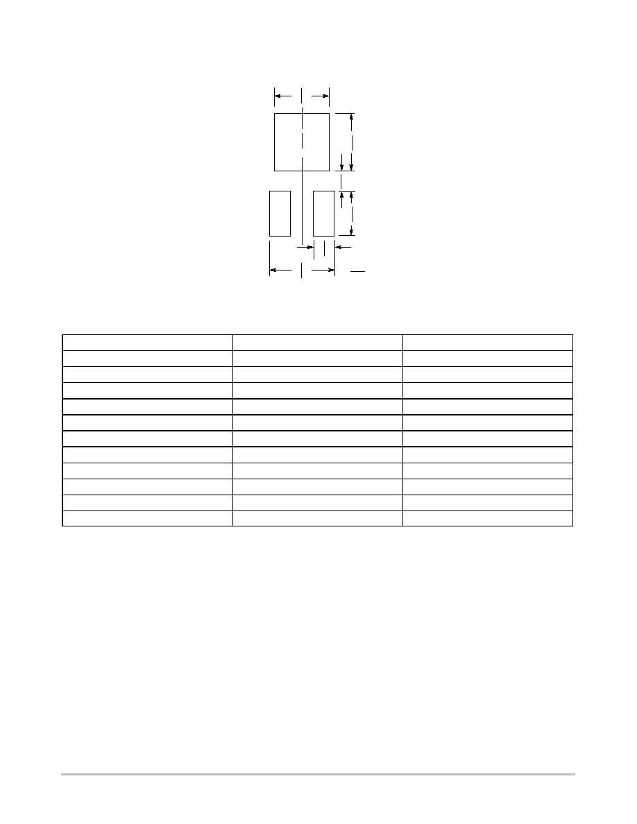
MINIMUM PAD SIZES RECOMMENDED FOR SURFACE MOUNTED APPLICATIONS
0.243 6.172
0.063 1.6
0.1
18
3.0
0.100 2.54
0.165 4.191
0.190 4.826
inches
mm
ORDERING INFORMATION
Device
Package
Shipping
MJD31C
DPAK
75 Units / Rail
MJD31CRL
DPAK
1800 Tape & Reel
MJD31CT4
DPAK
2500 Tape & Reel
MJD31C≠1
DPAK Straight Leads
75 Units / Rail
MJD31T4
DPAK
2500 Tape & Reel
MJD32C
DPAK
75 Units / Rail
MJD32CRL
DPAK
1800 Tape & Reel
MJD32CT4
DPAK
2500 Tape & Reel
MJD32C≠1
DPAK Straight Leads
75 Units / Rail
MJD32RL
DPAK
1800 Tape & Reel
MJD32T4
DPAK
2500 Tape & Reel