 | –≠–ª–µ–∫—Ç—Ä–æ–Ω–Ω—ã–π –∫–æ–º–ø–æ–Ω–µ–Ω—Ç: MJW21194 | –°–∫–∞—á–∞—Ç—å:  PDF PDF  ZIP ZIP |

©
Semiconductor Components Industries, LLC, 2002
March, 2002 ≠ Rev. 1
1
Publication Order Number:
MJW21193/D
MJW21193 (PNP)
MJW21194 (NPN)
Preferred Devices
Silicon Power Transistors
The MJW21193 and MJW21194 utilize Perforated Emitter
technology and are specifically designed for high power audio output,
disk head positioners and linear applications.
∑
Total Harmonic Distortion Characterized
∑
High DC Current Gain ≠
hFE = 20 Min @ IC = 8 Adc
∑
Excellent Gain Linearity
∑
High SOA: 2.25 A, 80 V, 1 Second
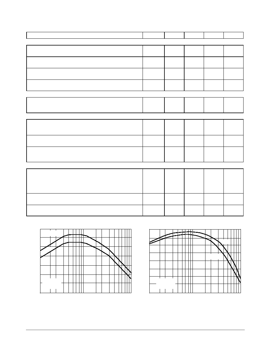
MAXIMUM RATINGS
Rating
Symbol
Value
Unit
Collector≠Emitter Voltage
VCEO
250
Vdc
Collector≠Base Voltage
VCBO
400
Vdc
Emitter≠Base Voltage
VEBO
5.0
Vdc
Collector≠Emitter Voltage ≠ 1.5 V
VCEX
400
Vdc
Collector Current ≠ Continuous
Collector Current
≠
Peak (Note 1)
IC
16
30
Adc
Base Current ≠ Continuous
IB
5.0
Adc
Total Power Dissipation @ TC = 25
∞
C
Derate Above 25
∞
C
PD
200
1.43
Watts
W/
∞
C
Operating and Storage Junction
Temperature Range
TJ, Tstg
≠65 to
+150
∞
C
THERMAL CHARACTERISTICS
Characteristic
Symbol
Max
Unit
Thermal Resistance,
Junction to Case
R
JC
0.7
∞
C/W
Thermal Resistance,
Junction to Ambient
R
JA
40
∞
C/W
1. Pulse Test: Pulse Width = 5
m
s, Duty Cycle
10%.
Device
Package
Shipping
ORDERING INFORMATION
MJW21193
TO≠247
http://onsemi.com
TO≠247
CASE 340K
STYLE 3
30 Units/Rail
2
1
16 AMPERES
COMPLEMENTARY
SILICON POWER
TRANSISTORS
250 VOLTS
200 WATTS
3
MARKING DIAGRAM
MJW
2119x
LLYWW
MJW2119x = Device Code
x
= 3 or 4
LL
= Location Code
Y
= Year
WW
= Work Week
Preferred devices are recommended choices for future use
and best overall value.
MJW21194
TO≠247
30 Units/Rail
1 BASE
2 COLLECTOR
3 EMITTER
MJW21193 (PNP) MJW21194 (NPN)
http://onsemi.com
2
ELECTRICAL CHARACTERISTICS
(TC = 25
∞
C unless otherwise noted)
Characteristic
Symbol
Min
Typ
Max
Unit
OFF CHARACTERISTICS
Collector≠Emitter Sustaining Voltage
(IC = 100 mAdc, IB = 0)
VCEO(sus)
250
≠
≠
Vdc
Collector Cutoff Current
(VCE = 200 Vdc, IB = 0)
ICEO
≠
≠
100
µ
Adc
Emitter Cutoff Current
(VCE = 5 Vdc, IC = 0)
IEBO
≠
≠
100
µ
Adc
Collector Cutoff Current
(VCE = 250 Vdc, VBE(off) = 1.5 Vdc)
ICEX
≠
≠
100
µ
Adc
SECOND BREAKDOWN
Second Breakdown Collector Current with Base Forward Biased
(VCE = 50 Vdc, t = 1 s (non≠repetitive)
(VCE = 80 Vdc, t = 1 s (non≠repetitive)
IS/b
4.0
2.25
≠
≠
≠
≠
Adc
ON CHARACTERISTICS
DC Current Gain
(IC = 8 Adc, VCE = 5 Vdc)
(IC = 16 Adc, IB = 5 Adc)
hFE
20
8
≠
≠
60
≠
Base≠Emitter On Voltage
(IC = 8 Adc, VCE = 5 Vdc)
VBE(on)
≠
≠
2.2
Vdc
Collector≠Emitter Saturation Voltage
(IC = 8 Adc, IB = 0.8 Adc)
(IC = 16 Adc, IB = 3.2 Adc)
VCE(sat)
≠
≠
≠
≠
1.4
4
Vdc
DYNAMIC CHARACTERISTICS
Total Harmonic Distortion at the Output
VRMS = 28.3 V, f = 1 kHz, PLOAD = 100 WRMS
hFE
unmatched
(Matched pair hFE = 50 @ 5 A/5 V)
hFE
matched
THD
≠
≠
0.8
0.08
≠
≠
%
Current Gain Bandwidth Product
(IC = 1 Adc, VCE = 10 Vdc, ftest = 1 MHz)
fT
4
≠
≠
MHz
Output Capacitance
(VCB = 10 Vdc, IE = 0, ftest = 1 MHz)
Cob
≠
≠
500
pF
IC COLLECTOR CURRENT (AMPS)
Figure 1. Typical Current Gain
Bandwidth Product
Figure 2. Typical Current Gain
Bandwidth Product
f, CURRENT
GAIN BANDWIDTH PRODUCT
(MHz)
T
PNP MJW21193
f, CURRENT
GAIN BANDWIDTH PRODUCT
(MHz)
T
NPN MJW21194
IC COLLECTOR CURRENT (AMPS)
6.5
6.0
5.5
5.0
4.5
4.0
3.5
3.0
1.0
10
0.1
8.0
7.0
6.0
5.0
4.0
3.0
2.0
0
1.0
10
0.1
1.0
VCE = 10 V
5 V
TJ = 25
∞
C
ftest = 1 MHz
10 V
VCE = 5 V
TJ = 25
∞
C
ftest = 1 MHz

MJW21193 (PNP) MJW21194 (NPN)
http://onsemi.com
3
Figure 3. DC Current Gain, VCE = 20 V
Figure 4. DC Current Gain, VCE = 20 V
Figure 5. DC Current Gain, VCE = 5 V
Figure 6. DC Current Gain, VCE = 5 V
h FE
, DC CURRENT
GAIN
IC COLLECTOR CURRENT (AMPS)
IC COLLECTOR CURRENT (AMPS)
h FE
, DC CURRENT
GAIN
h FE
, DC CURRENT
GAIN
IC COLLECTOR CURRENT (AMPS)
IC COLLECTOR CURRENT (AMPS)
VCE, COLLECTOR-EMITTER VOLTAGE (VOLTS)
Figure 7. Typical Output Characteristics
I C
, COLLECT
OR CURRENT
(A)
VCE, COLLECTOR-EMITTER VOLTAGE (VOLTS)
Figure 8. Typical Output Characteristics
I C
, COLLECT
OR CURRENT
(A)
PNP MJW21193
NPN MJW21194
h FE
, DC CURRENT
GAIN
TYPICAL CHARACTERISTICS
PNP MJW21193
PNP MJW21193
NPN MJW21194
NPN MJW21194
1000
100
10
100
10
1.0
0.1
1000
100
10
100
10
1.0
0.1
1000
100
10
100
10
1.0
0.1
1000
100
10
100
10
1.0
0.1
30
0
25
20
15
10
5.0
0
5.0
10
15
20
25
35
0
30
25
20
15
5.0
0
5.0
10
15
20
25
10
VCE = 20 V
TJ = 100
∞
C
25
∞
C
-25
∞
C
VCE = 20 V
TJ = 100
∞
C
25
∞
C
-25
∞
C
TJ = 100
∞
C
25
∞
C
-25
∞
C
VCE = 5 V
TJ = 100
∞
C
25
∞
C
-25
∞
C
VCE = 20 V
TJ = 25
∞
C
TJ = 25
∞
C
1.5 A
IB = 2 A
1 A
0.5 A
IB = 2 A
1.5 A
1 A
0.5 A

MJW21193 (PNP) MJW21194 (NPN)
http://onsemi.com
4
V BE(on)
, BASE-EMITTER VOL
T
AGE (VOL
TS)
Figure 9. Typical Saturation Voltages
IC, COLLECTOR CURRENT (AMPS)
SA
TURA
TION VOL
T
AGE (VOL
TS)
Figure 10. Typical Saturation Voltages
IC, COLLECTOR CURRENT (AMPS)
SA
TURA
TION VOL
T
AGE (VOL
TS)
Figure 11. Typical Base≠Emitter Voltage
IC, COLLECTOR CURRENT (AMPS)
Figure 12. Typical Base≠Emitter Voltage
IC, COLLECTOR CURRENT (AMPS)
V BE(on)
, BASE-EMITTER VOL
T
AGE (VOL
TS)
PNP MJW21193
NPN MJW21194
TYPICAL CHARACTERISTICS
PNP MJW21193
NPN MJW21194
3.0
2.5
2.0
1.5
1.0
0.5
0
100
10
1.0
0.1
1.4
100
10
1.0
0.1
1.2
1.0
0.8
0.6
0.4
0.2
0
10
100
10
1.0
0.1
1.0
0.1
10
100
10
1.0
0.1
1.0
0.1
TJ = 25
∞
C
IC/IB = 10
VBE(sat)
VCE(sat)
TJ = 25
∞
C
IC/IB = 10
VBE(sat)
VCE(sat)
TJ = 25
∞
C
VCE = 20 V (SOLID)
VCE = 5 V (DASHED)
TJ = 25
∞
C
VCE = 20 V (SOLID)
VCE = 5 V (DASHED)
Figure 13. Active Region Safe Operating Area
VCE, COLLECTOR EMITTER (VOLTS)
Figure 14. Active Region Safe Operating Area
PNP MJW21193
NPN MJW21194
100
1000
10
1.0
1.0
0.1
100
10
I C
, COLLECT
OR CURRENT (AMPS)
100 mSec
10 mSec
1 Sec
VCE, COLLECTOR EMITTER (VOLTS)
100
1000
10
1.0
1.0
0.1
100
10
I C
, COLLECT
OR CURRENT (AMPS)
100 mSec
10 mSec
1 Sec

MJW21193 (PNP) MJW21194 (NPN)
http://onsemi.com
5
There are two limitations on the power handling ability of
a transistor; average junction temperature and secondary
breakdown. Safe operating area curves indicate IC ≠ VCE
limits of the transistor that must be observed for reliable
operation; i.e., the transistor must not be subjected to greater
dissipation than the curves indicate.
The data of Figure 13 is based on TJ(pk) = 150
∞
C; TC is
variable depending on conditions. At high case
temperatures,
thermal limitations will reduce the power than
can be handled to values less than the limitations imposed by
second breakdown.
Figure 15. MJW21193 Typical Capacitance
VR, REVERSE VOLTAGE (VOLTS)
C, CAP
ACIT
ANCE (pF)
Figure 16. MJW21194 Typical Capacitance
VR, REVERSE VOLTAGE (VOLTS)
C, CAP
ACIT
ANCE (pF)
Figure 17. Typical Total Harmonic Distortion
FREQUENCY (Hz)
T HD
, T
O
T
A
L
HARMONIC
DIST
OR
TION (%)
10000
1000
100
100
10
1.0
0.1
10000
1000
100
100
10
1.0
0.1
1.2
1.1
1.0
0.9
0.8
0.7
0.6
100000
10000
1000
100
10
TC = 25
∞
C
Cob
Cib
TC = 25
∞
C
Cib
Cob
f(test) = 1 MHz)
f(test) = 1 MHz)