©
Semiconductor Components Industries, LLC, 2000
April, 2000 ≠ Rev. 1
1
Publication Order Number:
MMBD6100LT1/D
MMBD6100LT1
Monolithic Dual
Switching Diode
MAXIMUM RATINGS (EACH DIODE)
Symbol
Rating
Value
Unit
V
R
Reverse Voltage
70
Vdc
I
F
Forward Current
200
mAdc
I
FM(surge)
Peak Forward Surge Current
500
mAdc
THERMAL CHARACTERISTICS
Symbol
Characteristic
Max
Unit
P
D
Total Device Dissipation, FR≠5 Board
(1)
T
A
= 25
∞
C
Derate above 25
∞
C
225
1.8
mW
mW/
∞
C
R
q
JA
Thermal Resistance, Junction to Ambient
556
∞
C/W
P
D
Total Device Dissipation
Alumina Substrate,
(2)
T
A
= 25
∞
C
Derate above 25
∞
C
300
2.4
mW
mW/
∞
C
R
q
JA
Thermal Resistance, Junction to Ambient
417
∞
C/W
T
J
, T
stg
Junction and Storage
Temperature Range
≠55 to
+150
∞
C
(1) FR≠ 5 = 1.0
0.75
0.062 in.
(2) Alumina = 0.4
0.3
0.024 in. 99.5% alumina.
Device
Package
Shipping
ORDERING INFORMATION
MMBD6100LT1
SOT≠23S
3000/Tape & Reel
http://onsemi.com
PLASTIC
SOT≠23S
CASE 318
1
2
3
3
CATHODE
2
ANODE
ANODE
1
MMBD6100LT3
SOT≠23S
10,000/Tape & Reel
DEVICE MARKING
5BM
MMBD6100LT1
http://onsemi.com
4
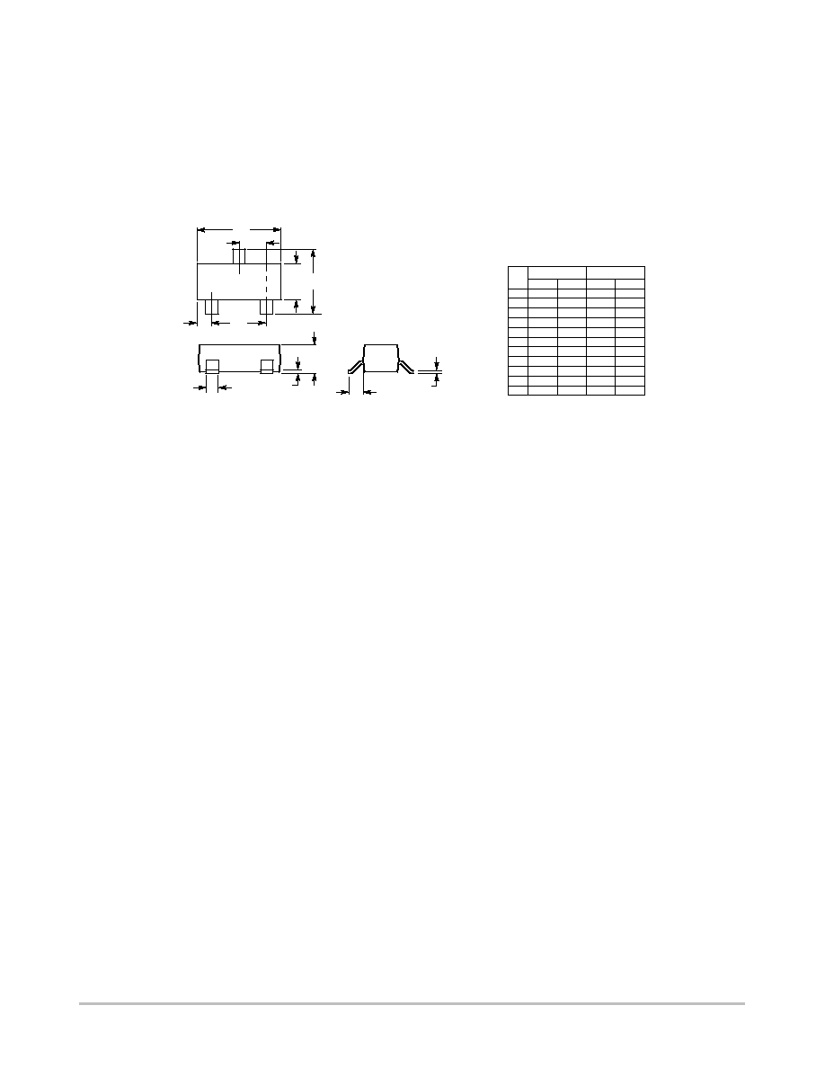
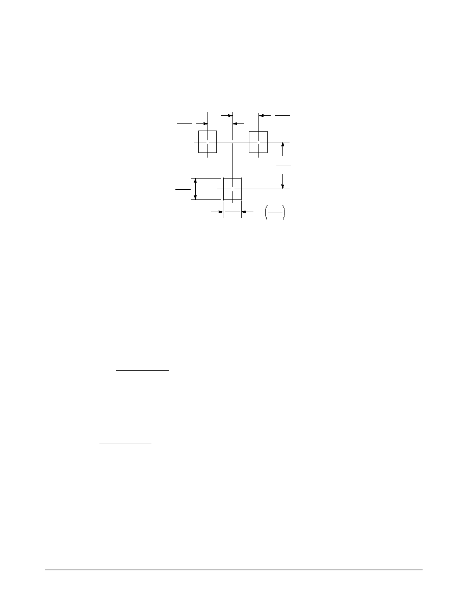
INFORMATION FOR USING THE SOT≠23 SURFACE MOUNT PACKAGE
MINIMUM RECOMMENDED FOOTPRINT FOR SURFACE MOUNTED APPLICATIONS
Surface mount board layout is a critical portion of the
total design. The footprint for the semiconductor packages
must be the correct size to insure proper solder connection
interface between the board and the package. With the
correct pad geometry, the packages will self align when
subjected to a solder reflow process.
SOT≠23
mm
inches
0.037
0.95
0.037
0.95
0.079
2.0
0.035
0.9
0.031
0.8
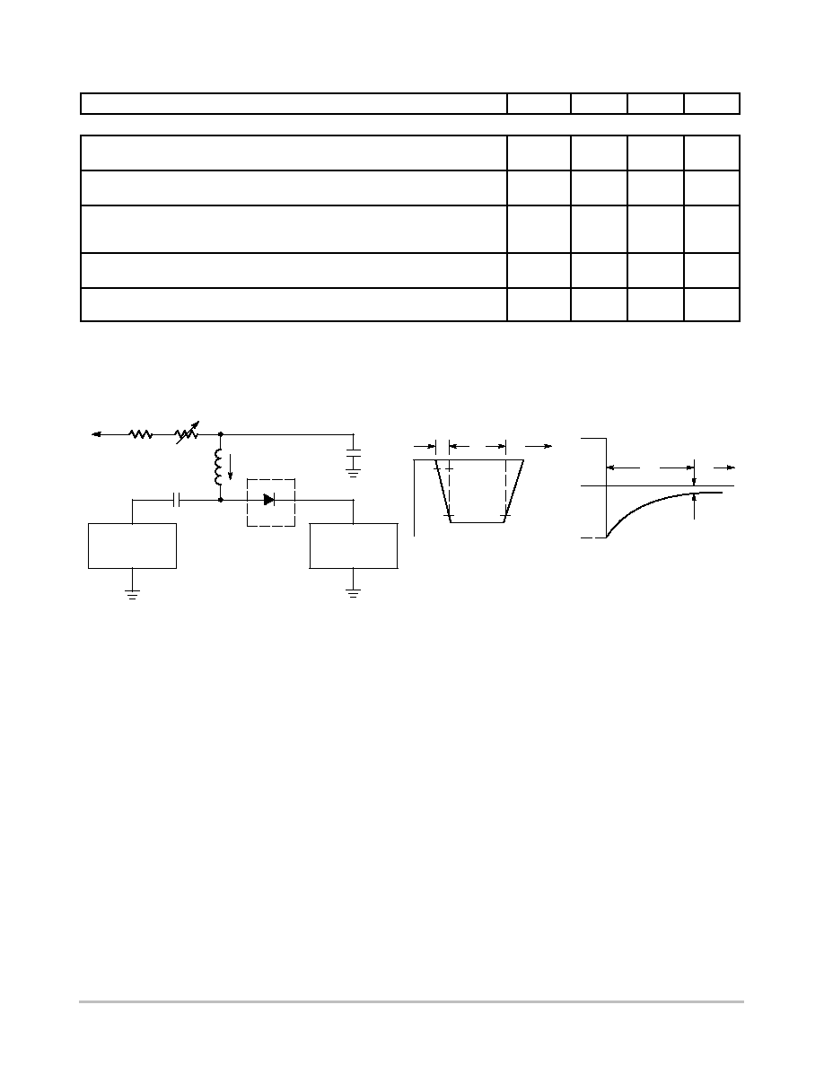
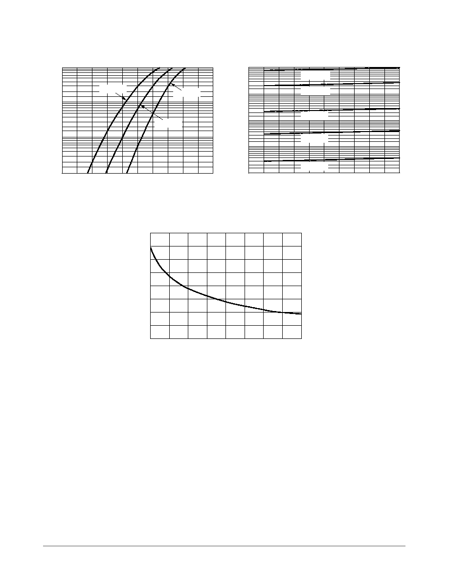
SOT≠23 POWER DISSIPATION
The power dissipation of the SOT≠23 is a function of the
pad size. This can vary from the minimum pad size for
soldering to a pad size given for maximum power
dissipation. Power dissipation for a surface mount device is
determined by T
J(max)
, the maximum rated junction
temperature of the die, R
JA
, the thermal resistance from
the device junction to ambient, and the operating
temperature, T
A
. Using the values provided on the data
sheet for the SOT≠23 package, P
D
can be calculated as
follows:
P
D
=
T
J(max)
≠ T
A
R
JA
The values for the equation are found in the maximum
ratings table on the data sheet. Substituting these values
into the equation for an ambient temperature T
A
of 25
∞
C,
one can calculate the power dissipation of the device which
in this case is 225 milliwatts.
P
D
=
150
∞
C ≠ 25
∞
C
556
∞
C/W
= 225 milliwatts
The 556
∞
C/W for the SOT≠23 package assumes the use
of the recommended footprint on a glass epoxy printed
circuit board to achieve a power dissipation of 225
milliwatts. There are other alternatives to achieving higher
power dissipation from the SOT≠23 package. Another
alternative would be to use a ceramic substrate or an
aluminum core board such as Thermal Clad
TM
. Using a
board material such as Thermal Clad, an aluminum core
board, the power dissipation can be doubled using the same
footprint.
SOLDERING PRECAUTIONS
The melting temperature of solder is higher than the rated
temperature of the device. When the entire device is heated
to a high temperature, failure to complete soldering within
a short time could result in device failure. Therefore, the
following items should always be observed in order to
minimize the thermal stress to which the devices are
subjected.
∑
Always preheat the device.
∑
The delta temperature between the preheat and
soldering should be 100
∞
C or less.*
∑
When preheating and soldering, the temperature of the
leads and the case must not exceed the maximum
temperature ratings as shown on the data sheet. When
using infrared heating with the reflow soldering
method, the difference shall be a maximum of 10
∞
C.
∑
The soldering temperature and time shall not exceed
260
∞
C for more than 10 seconds.
∑
When shifting from preheating to soldering, the
maximum temperature gradient shall be 5
∞
C or less.
∑
After soldering has been completed, the device should
be allowed to cool naturally for at least three minutes.
Gradual cooling should be used as the use of forced
cooling will increase the temperature gradient and
result in latent failure due to mechanical stress.
∑
Mechanical stress or shock should not be applied
during cooling.
* Soldering a device without preheating can cause
excessive thermal shock and stress which can result in
damage to the device.