Äîêóìåíòàöèÿ è îïèñàíèÿ www.docs.chipfind.ru
©
Semiconductor Components Industries, LLC, 2000
November, 2000 Rev. 2
1
Publication Order Number:
MMBF0201NLT1/D
MMBF0201NLT1
Preferred Device
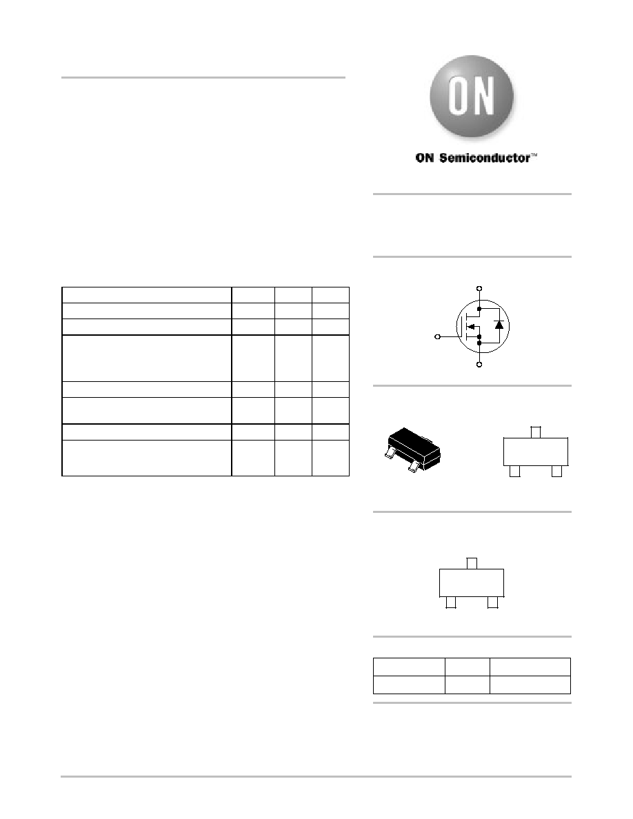
Power MOSFET
300 mAmps, 20 Volts
NChannel SOT23
These miniature surface mount MOSFETs low RDS(on) assure
minimal power loss and conserve energy, making these devices ideal
for use in small power management circuitry. Typical applications are
d c d c c o n v e r t e r s , p o w e r m a n a g e m e n t i n p o r t a b l e a n d
batterypowered products such as computers, printers, PCMCIA
cards, cellular and cordless telephones.
·
Low RDS(on) Provides Higher Efficiency and Extends Battery Life
·
Miniature SOT23 Surface Mount Package Saves Board Space
MAXIMUM RATINGS
(TJ = 25
°
C unless otherwise noted)
Rating
Symbol
Value
Unit
DraintoSource Voltage
VDSS
20
Vdc
GatetoSource Voltage Continuous
VGS
±
20
Vdc
Drain Current
Continuous @ TA = 25
°
C
Continuous @ TA = 70
°
C
Pulsed Drain Current (tp
10
µ
s)
ID
ID
IDM
300
240
750
mAdc
Total Power Dissipation @ TA = 25
°
C(1)
PD
225
mW
Operating and Storage Temperature
Range
TJ, Tstg
55 to
150
°
C
Thermal Resistance JunctiontoAmbient
R
JA
556
°
C/W
Maximum Lead Temperature for Soldering
Purposes, 1/8
from case for 10
seconds
TL
260
°
C
3
1
2
Device
Package
Shipping
ORDERING INFORMATION
MMBF0201NLT1
SOT23
3000 Tape & Reel
NChannel
SOT23
CASE 318
STYLE 21
http://onsemi.com
W
MARKING
DIAGRAM
N1
W
= Work Week
PIN ASSIGNMENT
3
2
1
Drain
Gate
2
1
3
Source
300 mAMPS
20 VOLTS
RDS(on) = 1
W
Preferred devices are recommended choices for future use
and best overall value.
MMBF0201NLT1
http://onsemi.com
2
ELECTRICAL CHARACTERISTICS
(TA = 25
°
C unless otherwise noted)
Characteristic
Symbol
Min
Typ
Max
Unit
OFF CHARACTERISTICS
DraintoSource Breakdown Voltage
(VGS = 0 Vdc, ID = 10
µ
A)
V(BR)DSS
20
Vdc
Zero Gate Voltage Drain Current
(VDS = 16 Vdc, VGS = 0 Vdc)
(VDS = 16 Vdc, VGS = 0 Vdc, TJ = 125
°
C)
IDSS
1.0
10
µ
Adc
GateBody Leakage Current (VGS =
±
20 Vdc, VDS = 0)
IGSS
±
100
nAdc
ON CHARACTERISTICS (Note 1.)
Gate Threshold Voltage
(VDS = VGS, ID = 250
µ
Adc)
VGS(th)
1.0
1.7
2.4
Vdc
Static DraintoSource OnResistance
(VGS = 10 Vdc, ID = 300 mAdc)
(VGS = 4.5 Vdc, ID = 100 mAdc)
rDS(on)
0.75
1.0
1.0
1.4
Ohms
Forward Transconductance (VDS = 10 Vdc, ID = 200 mAdc)
gFS
450
mMhos
DYNAMIC CHARACTERISTICS
Input Capacitance
(VDS = 5.0 V)
Ciss
45
pF
Output Capacitance
(VDS = 5.0 V)
Coss
25
Transfer Capacitance
(VDG = 5.0 V)
Crss
5.0
SWITCHING CHARACTERISTICS (Note 2.)
TurnOn Delay Time
td(on)
2.5
ns
Rise Time
(VDD = 15 Vdc, ID = 300 mAdc,
tr
2.5
TurnOff Delay Time
(VDD 15 Vdc, ID 300 mAdc,
RL = 50
)
td(off)
15
Fall Time
tf
0.8
Gate Charge (See Figure 5)
QT
1400
pC
SOURCEDRAIN DIODE CHARACTERISTICS
Continuous Current
IS
0.3
A
Pulsed Current
ISM
0.75
Forward Voltage (Note 2.)
VSD
0.85
V
1. Pulse Test: Pulse Width
300
µ
s, Duty Cycle
2%.
2. Switching characteristics are independent of operating junction temperature.
MMBF0201NLT1
http://onsemi.com
3
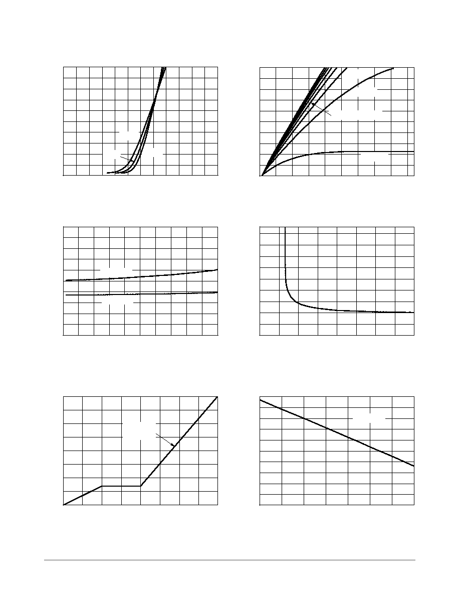
TYPICAL ELECTRICAL CHARACTERISTICS
R DS(on)
, DRAIN-T
O-SOURCE RESIST
ANCE (OHMS)
ON-RESIST
ANCE (OHMS)
0
1
2
3
4
6
0
0.6
0.8
1.0
VGS, GATE-TO-SOURCE VOLTAGE (VOLTS)
Figure 1. Transfer Characteristics
I D
, DRAIN CURRENT
(AMPS)
0
0.3
0.6
0.9
1.2
1.4
0
0.6
0.8
1.0
I D
, DRAIN CURRENT
(AMPS)
VDS, DRAIN-TO-SOURCE VOLTAGE (VOLTS)
Figure 2. OnRegion Characteristics
0
0.2
0.4
1
0
0.3
0.9
1.2
1.5
0
5
10
20
0
1.0
1.5
2.0
2.4
ID, DRAIN CURRENT (AMPS)
Figure 3. OnResistance versus Drain Current
VGS, GATE-TO-SOURCE VOLTAGE (VOLTS)
Figure 4. OnResistance versus
GatetoSource Voltage
0
10
12
14
16
-25
25
100
150
0.60
1.10
Qg, TOTAL GATE CHARGE (pC)
Figure 5. Gate Charge
TEMPERATURE (
°
C)
Figure 6. Threshold Voltage Variance
Over Temperature
5
0.4
0.4
0.6
0.6
0.8
15
0
160
450
2000
0.2
125
°
C
25
°
C
-55
°
C
0.2
VGS = 5 V
VGS = 4 V
VGS = 3 V
VGS = 4.5 V
VGS = 10 V
0.5
V GS
, GA
TE-T
O-SOURCE VOL
T
AGE (VOL
TS)
2
4
6
8
3400
VDS = 16 V
ID = 300 mA
V GS(th)
, NORMALIZED
ID = 250
µ
A
1.05
1.00
0.95
0.90
0.85
0.80
0.75
0.70
0.65
0
50
75
125
VGS = 10, 9, 8, 7, 6 V
MMBF0201NLT1
http://onsemi.com
4
TYPICAL ELECTRICAL CHARACTERISTICS
SOURCE CURRENT
(AMPS)
-50
-25
0
25
50
150
0.6
1.4
1.6
1.8
TJ, JUNCTION TEMPERATURE (
°
C)
Figure 7. OnResistance versus
Junction Temperature
0
5
10
15
20
0
60
80
100
VDS, DRAIN-TO-SOURCE VOLTAGE (VOLTS)
Figure 8. Capacitance
0
0.3
0.6
1.4
0.001
0.1
1.0
10
SOURCE-TO-DRAIN FORWARD VOLTAGE (VOLTS)
Figure 9. SourcetoDrain Forward Voltage
versus Continuous Current (IS)
75
1.2
40
0.01
0.9
1.2
1.0
20
R DS(on)
, NORMALIZED (OHMS)
0.8
100
125
VGS = 10 V @ 300 mA
VGS = 4.5 V @ 100 mA
C, CAP
ACIT
ANCE (pF)
Ciss
Coss
Crss
125
°
C
25
°
C
-55
°
C
MMBF0201NLT1
http://onsemi.com
5
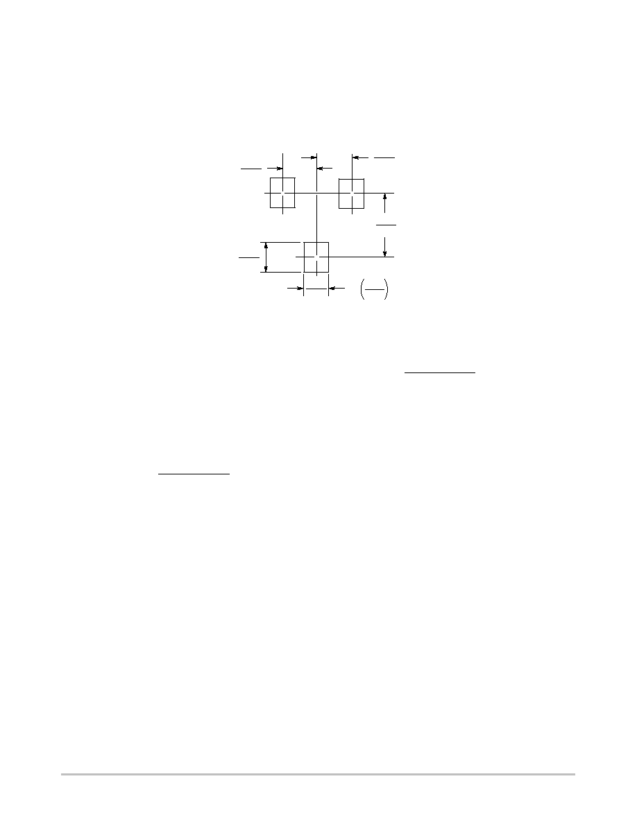
INFORMATION FOR USING THE SOT23 SURFACE MOUNT PACKAGE
MINIMUM RECOMMENDED FOOTPRINT FOR SURFACE MOUNTED APPLICATIONS
Surface mount board layout is a critical portion of the
total design. The footprint for the semiconductor packages
must be the correct size to insure proper solder connection
interface between the board and the package. With the
correct pad geometry, the packages will self align when
subjected to a solder reflow process.
mm
inches
0.037
0.95
0.037
0.95
0.079
2.0
0.035
0.9
0.031
0.8
SOT23 POWER DISSIPATION
The power dissipation of the SOT23 is a function of the
drain pad size. This can vary from the minimum pad size
for soldering to a pad size given for maximum power
dissipation. Power dissipation for a surface mount device is
determined by TJ(max), the maximum rated junction
temperature of the die, R
JA, the thermal resistance from
the device junction to ambient, and the operating
temperature, TA. Using the values provided on the data
sheet for the SOT23 package, PD can be calculated as
follows:
PD =
TJ(max) TA
R
JA
The values for the equation are found in the maximum
ratings table on the data sheet. Substituting these values
into the equation for an ambient temperature TA of 25
°
C,
one can calculate the power dissipation of the device which
in this case is 225 milliwatts.
PD =
150
°
C 25
°
C
556
°
C/W
= 225 milliwatts
The 556
°
C/W for the SOT23 package assumes the use
of the recommended footprint on a glass epoxy printed
circuit board to achieve a power dissipation of 225
milliwatts. There are other alternatives to achieving higher
power dissipation from the SOT23 package. Another
alternative would be to use a ceramic substrate or an
aluminum core board such as Thermal Clad
t. Using a
board material such as Thermal Clad, an aluminum core
board, the power dissipation can be doubled using the same
footprint.
SOLDERING PRECAUTIONS
The melting temperature of solder is higher than the rated
temperature of the device. When the entire device is heated
to a high temperature, failure to complete soldering within
a short time could result in device failure. Therefore, the
following items should always be observed in order to
minimize the thermal stress to which the devices are
subjected.
·
Always preheat the device.
·
The delta temperature between the preheat and
soldering should be 100
°
C or less.*
·
When preheating and soldering, the temperature of the
leads and the case must not exceed the maximum
temperature ratings as shown on the data sheet. When
using infrared heating with the reflow soldering
method, the difference should be a maximum of 10
°
C.
·
The soldering temperature and time should not exceed
260
°
C for more than 10 seconds.
·
When shifting from preheating to soldering, the
maximum temperature gradient should be 5
°
C or less.
·
After soldering has been completed, the device should
be allowed to cool naturally for at least three minutes.
Gradual cooling should be used as the use of forced
cooling will increase the temperature gradient and
result in latent failure due to mechanical stress.
·
Mechanical stress or shock should not be applied
during cooling
* Soldering a device without preheating can cause
excessive thermal shock and stress which can result in
damage to the device.