©
Semiconductor Components Industries, LLC, 2004
December, 2004 - Rev. 4
1
Publication Order Number:
MMBT5550LT1/D
MMBT5550LT1,
MMBT5551LT1
MMBT5551LT1 is a Preferred Device
High Voltage Transistors
NPN Silicon
Features
∑
Pb-Free Packages are Available
MAXIMUM RATINGS
Rating
Symbol
5550
5551
Unit
Collector - Emitter Voltage
V
CEO
140
160
Vdc
Collector - Base Voltage
V
CBO
160
180
Vdc
Emitter - Base Voltage
V
EBO
6.0
Vdc
Collector Current - Continuous
I
C
600
mAdc
Maximum ratings are those values beyond which device damage can occur.
Maximum ratings applied to the device are individual stress limit values (not
normal operating conditions) and are not valid simultaneously. If these limits
are exceeded, device functional operation is not implied, damage may occur
and reliability may be affected.
THERMAL CHARACTERISTICS
Characteristic
Symbol
Max
Unit
Total Device Dissipation
FR- 5 Board (Note 1)
T
A
= 25
∞
C
Derate Above 25
∞
C
P
D
225
1.8
mW
mW/
∞
C
Thermal Resistance,
Junction-to-Ambient
R
q
JA
556
∞
C/W
Total Device Dissipation
Alumina Substrate (Note 2)
T
A
= 25
∞
C
Derate Above 25
∞
C
P
D
300
2.4
mW
mW/
∞
C
Thermal Resistance,
Junction-to-Ambient
R
q
JA
417
∞
C/W
Junction and Storage Temperature
T
J
, T
stg
- 55 to +150
∞
C
1. FR- 5 = 1.0
0.75
0.062 in.
2. Alumina = 0.4
0.3
0.024 in. 99.5% alumina.
Preferred devices are recommended choices for future use
and best overall value.
Device
Package
Shipping
ORDERING INFORMATION
MMBT5550LT1
SOT-23
3000 Tape & Reel
MMBT5551LT1
SOT-23
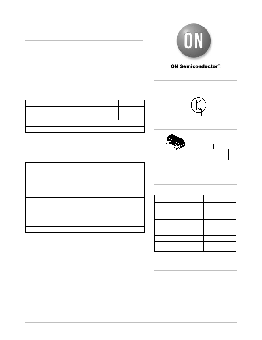
SOT-23 (TO-236)
CASE 318
STYLE 6
3000 Tape & Reel
MARKING
DIAGRAM
xxx = MMBT550LT1 = M1F,
MMBT5551LT1, LT3, LT1G = G1
M
= Month Code
COLLECTOR
3
1
BASE
2
EMITTER
xxxM
MMBT5551LT3G
SOT-23
(Pb-Free)
10,000 Tape & Reel
For information on tape and reel specifications,
including part orientation and tape sizes, please
refer to our Tape and Reel Packaging Specifications
Brochure, BRD8011/D.
MMBT5551LT1G
SOT-23
(Pb-Free)
3000 Tape & Reel
MMBT5551LT3
SOT-23
10,000 Tape & Reel
MMBT5550LT1G
SOT-23
(Pb-Free)
3000 Tape & Reel
http://onsemi.com
MMBT5550LT1, MMBT5551LT1
http://onsemi.com
2
ELECTRICAL CHARACTERISTICS
(T
A
= 25
∞
C unless otherwise noted)
Characteristic
Symbol
Min
Max
Unit
OFF CHARACTERISTICS
Collector - Emitter Breakdown Voltage (Note 3)
(I
C
= 1.0 mAdc, I
B
= 0)
MMBT5550
MMBT5551
V
(BR)CEO
140
160
-
-
Vdc
Collector - Base Breakdown Voltage
(I
C
= 100
m
Adc, I
E
= 0)
MMBT5550
MMBT5551
V
(BR)CBO
160
180
-
-
Vdc
Emitter - Base Breakdown Voltage
(I
E
= 10
m
Adc, I
C
= 0)
V
(BR)EBO
6.0
-
Vdc
Collector Cutoff Current
(V
CB
= 100 Vdc, I
E
= 0)
MMBT5550
(V
CB
= 120 Vdc, I
E
= 0)
MMBT5551
(V
CB
= 100 Vdc, I
E
= 0, T
A
= 100
∞
C)
MMBT5550
(V
CB
= 120 Vdc, I
E
= 0, T
A
= 100
∞
C)
MMBT5551
I
CBO
-
-
-
-
100
50
100
50
nAdc
m
Adc
Emitter Cutoff Current
(V
EB
= 4.0 Vdc, I
C
= 0)
I
EBO
-
50
nAdc
ON CHARACTERISTICS
DC Current Gain
(I
C
= 1.0 mAdc, V
CE
= 5.0 Vdc)
MMBT5550
MMBT5551
(I
C
= 10 mAdc, V
CE
= 5.0 Vdc)
MMBT5550
MMBT5551
(I
C
= 50 mAdc, V
CE
= 5.0 Vdc)
MMBT5550
MMBT5551
h
FE
60
80
60
80
20
30
-
-
250
250
-
-
-
Collector - Emitter Saturation Voltage
(I
C
= 10 mAdc, I
B
= 1.0 mAdc)
Both Types
(I
C
= 50 mAdc, I
B
= 5.0 mAdc)
MMBT5550
MMBT5551
V
CE(sat)
-
-
-
0.15
0.25
0.20
Vdc
Base - Emitter Saturation Voltage
(I
C
= 10 mAdc, I
B
= 1.0 mAdc)
Both Types
(I
C
= 50 mAdc, I
B
= 5.0 mAdc)
MMBT5550
MMBT5551
V
BE(sat)
-
-
-
1.0
1.2
1.0
Vdc
Collector Emitter Cut-off
(V
CB
= 10 V)
Both Types
(V
CB
= 75 V)
I
CES
-
-
50
100
nA
3. Pulse Test: Pulse Width = 300
m
s, Duty Cycle = 2.0%.
MMBT5550LT1, MMBT5551LT1
http://onsemi.com
3
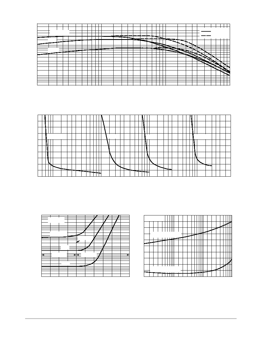
Figure 1. DC Current Gain
I
C
, COLLECTOR CURRENT (mA)
500
h , DC CURRENT
GAIN
FE
T
J
= 125
∞
C
-55
∞
C
25
∞
C
5.0
10
0.1
0.2
0.3
0.5
0.7
1.0
2.0
3.0
5.0
7.0
10
20
30
50
70
100
200
30
20
300
100
50
7.0
V
CE
= 1.0 V
V
CE
= 5.0 V
Figure 2. Collector Saturation Region
I
B
, BASE CURRENT (mA)
1.0
I
C
= 1.0 mA
0
0.3
0.005
0.01
0.2
0.5
1.0
2.0
20
50
0.8
0.5
0.4
0.9
0.7
0.6
0.2
0.02
0.05
0.1
10
V CE
, COLLECT
OR-EMITTER VOL
T
AGE (VOL
TS)
0.1
10 mA
30 mA
100 mA
5.0
Figure 3. Collector Cut-Off Region
V
BE
, BASE-EMITTER VOLTAGE (VOLTS)
10
1
10
-5
0.4
0.3
0.1
10
0
10
-1
10
-2
10
-3
10
-4
0.2
0
0.1
0.2
0.4
0.3
0.6
0.5
V
CE
= 30 V
T
J
= 125
∞
C
75
∞
C
25
∞
C
I
C
= I
CES
, COLLECT
OR CURRENT
(A)
µ
I C
REVERSE
FORWARD
I
C
, COLLECTOR CURRENT (mA)
1.0
V
,
VOL
T
AGE (VOL
TS)
1.0
2.0
5.0
10
20
50
100
T
J
= 25
∞
C
V
BE(sat)
@ I
C
/I
B
= 10
V
CE(sat)
@ I
C
/I
B
= 10
0.1
0.2
0.5
Figure 4. "On" Voltages
0.8
0.6
0.4
0.2
0
3.0
30
0.3
MMBT5550LT1, MMBT5551LT1
http://onsemi.com
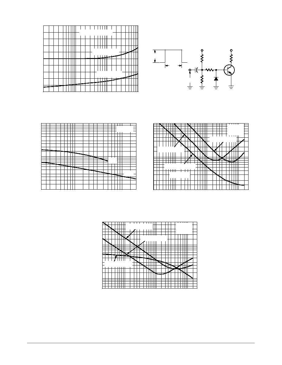
4
C, CAP
ACIT
ANCE (pF)
V
R
, REVERSE VOLTAGE (VOLTS)
100
1.0
0.2
0.5
1.0
2.0
5.0
10
20
C
ibo
70
50
30
20
10
7.0
5.0
3.0
2.0
0.3
0.7
3.0
7.0
C
obo
10.2 V
V
in
10 ms
INPUT PULSE
V
BB
-8.8 V
100
R
B
5.1 k
0.25 mF
V
in
100
1N914
V
out
R
C
V
CC
30 V
3.0 k
t
r
, t
f
10 ns
DUTY CYCLE = 1.0%
Values Shown are for I
C
@ 10 mA
T
J
= 25
∞
C
I
C
, COLLECTOR CURRENT (mA)
1000
0.3
1.0
10
20 30 50
0.5
0.2
t, TIME
(ns)
10
20
30
50
100
200
300
500
2.0
100
200
I
C
/I
B
= 10
T
J
= 25
∞
C
t
r
@ V
CC
= 120 V
3.0 5.0
t
r
@ V
CC
= 30 V
t
d
@ V
EB(off)
= 1.0 V
V
CC
= 120 V
I
C
, COLLECTOR CURRENT (mA)
5000
t, TIME
(ns)
50
100
200
300
500
3000
2000
1000
0.3
1.0
10
20 30 50
0.5
0.2
2.0
100
200
3.0 5.0
I
C
/I
B
= 10
T
J
= 25
∞
C
t
f
@ V
CC
= 120 V
t
f
@ V
CC
= 30 V
t
s
@ V
CC
= 120 V
I
C
, COLLECTOR CURRENT (mA)
2.5
q
VC
for V
CE(sat)
q
VB
for V
BE(sat)
Figure 5. Temperature Coefficients
T
J
= - 55
∞
C to +135
∞
C
V,
TEMPERA
TURE COEFFICIENT
(mV/
C)
∞
2.0
1.5
1.0
0.5
0
- 0.5
- 1.0
- 1.5
- 2.0
- 2.5
1.0
2.0
5.0
10
20
50
100
0.1
0.2
0.5
3.0
30
0.3
Figure 6. Switching Time Test Circuit
Figure 7. Capacitances
Figure 8. Turn-On Time
Figure 9. Turn-Off Time
MMBT5550LT1, MMBT5551LT1
http://onsemi.com
5
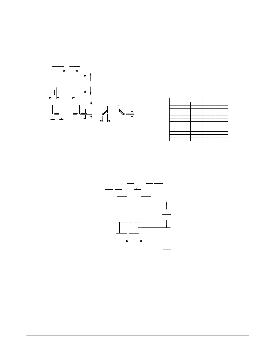
PACKAGE DIMENSIONS
STYLE 6:
PIN 1. BASE
2. EMITTER
3. COLLECTOR
SOT-23-3 (TO-236)
CASE 318-08
ISSUE AK
*For additional information on our Pb-Free strategy and soldering
details, please download the ON Semiconductor Soldering and
Mounting Techniques Reference Manual, SOLDERRM/D.
SOLDERING FOOTPRINT*
mm
inches
SCALE 10:1
0.8
0.031
0.9
0.035
0.95
0.037
0.95
0.037
2.0
0.079
D
J
K
L
A
C
B S
H
G
V
3
1
2
DIM
A
MIN
MAX
MIN
MAX
MILLIMETERS
0.1102
0.1197
2.80
3.04
INCHES
B
0.0472
0.0551
1.20
1.40
C
0.0350
0.0440
0.89
1.11
D
0.0150
0.0200
0.37
0.50
G
0.0701
0.0807
1.78
2.04
H
0.0005
0.0040
0.013
0.100
J
0.0034
0.0070
0.085
0.177
K
0.0140
0.0285
0.35
0.69
L
0.0350
0.0401
0.89
1.02
S
0.0830
0.1039
2.10
2.64
V
0.0177
0.0236
0.45
0.60
NOTES:
1. DIMENSIONING AND TOLERANCING PER ANSI
Y14.5M, 1982.
2. CONTROLLING DIMENSION: INCH.
3. MAXIMUM LEAD THICKNESS INCLUDES LEAD
FINISH THICKNESS. MINIMUM LEAD
THICKNESS IS THE MINIMUM THICKNESS OF
BASE MATERIAL.
4. 318-01 THRU -07 AND -09 OBSOLETE, NEW
STANDARD 318-08.