 | –≠–ª–µ–∫—Ç—Ä–æ–Ω–Ω—ã–π –∫–æ–º–ø–æ–Ω–µ–Ω—Ç: MSR1560 | –°–∫–∞—á–∞—Ç—å:  PDF PDF  ZIP ZIP |
©
Semiconductor Components Industries, LLC, 2000
October, 2000 ≠ Rev. 2
1
Publication Order Number:
MSR1560/D
MSR1560
SWITCHMODE
TM
Soft
Recovery Power Rectifier
Designed for boost converter or hard≠switched converter
applications, especially for Power Factor Correction application. It
could also be used as a free wheeling diode in variable speed motor
control applications and switching mode power supplies. These
state≠of≠the≠art devices have the following features:
∑
Soft Recovery with Low Reverse Recovery Charge (Q
RR
) and Peak
Reverse Recovery Current (I
RRM
)
∑
150
∞
C Operating Junction Temperature
∑
Popular TO≠220 Package
∑
Epoxy meets UL94, V
O
@ 1/8
∑
Low Forward Voltage
∑
Low Leakage Current
∑
High Temperature Glass Passivated Junction
Mechanical Characteristics:
∑
Case: Molded Epoxy
∑
Weight: 1.9 Grams (approximately)
∑
Finish: All External Surfaces Corrosion Resistant and Terminal
Leads Readily Solderable
∑
Lead Temperature for Soldering Purposes: 260
∞
C Max. for 10
Seconds
∑
Shipped in 50 Units per Plastic Tube
∑
Marking: MSR1560
SOFT RECOVERY POWER
RECTIFIER 15 AMPERES
600 VOLTS
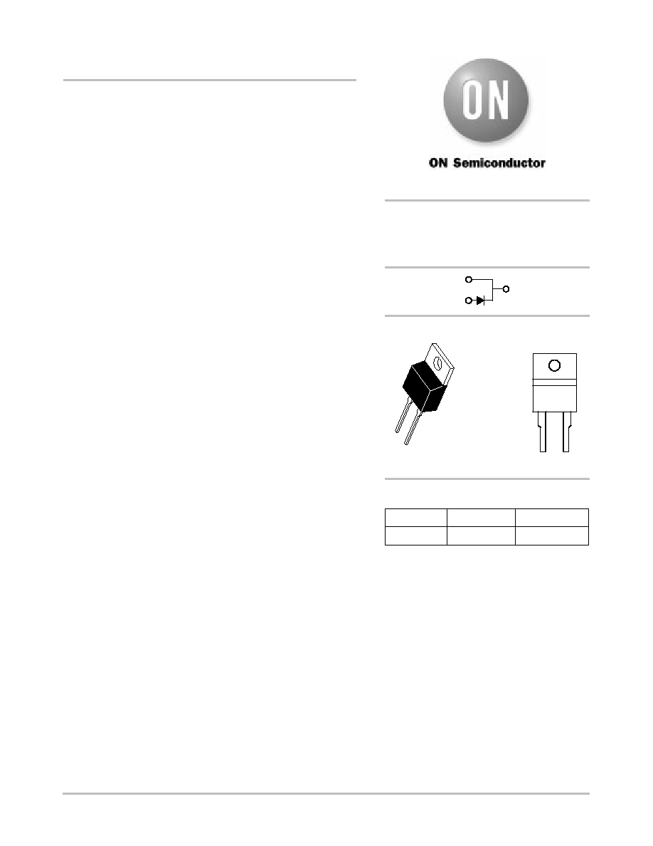
http://onsemi.com
MARKING
DIAGRAM
CASE 221B
TO≠220
PLASTIC
4
1
3
1
4
3
1
3
4
MSR1560
Device
Package
Shipping
ORDERING INFORMATION
MSR1560
TO≠220
50 Units/Rail

MSR1560
http://onsemi.com
2
MAXIMUM RATINGS
Rating
Symbol
Value
Unit
Peak Repetitive Reverse Voltage
Working Peak Reverse Voltage
DC Blocking Voltage
V
RRM
V
RWM
V
R
600
V
Average Rectified Forward Current (At Rated V
R
, T
C
= 125
∞
C)
I
O
15
A
Peak Repetitive Forward Current (At Rated V
R
, Square Wave, 20 kHz, T
C
= 125
∞
C)
I
FRM
30
A
Non≠Repetitive Peak Surge Current
(Surge applied at rated load conditions, halfwave, single phase, 60 Hz)
I
FSM
100
A
Storage / Operating Case Temperature
T
stg
, T
C
≠ 65 to 150
∞
C
Operating Junction Temperature
T
J
≠ 65 to 150
∞
C
THERMAL CHARACTERISTICS
Thermal Resistance -- Junction≠to≠Case
Thermal Resistance -- Junction≠to≠Ambient
R
q
JC
R
q
JA
1.6
72.8
∞
C/W
ELECTRICAL CHARACTERISTICS
Maximum Instantaneous Forward Voltage (Note 1.) (I
F
= 15 A)
V
F
T
J
= 25
∞
C
T
J
= 150
∞
C
V
a
u
s a a eous o
a d o age ( o e
) (
F
5
)
Typical
F
1.8
1.5
1.4
1.2
Maximum Instantaneous Reverse Current (V
R
= 600 V)
I
R
T
J
= 25
∞
C
T
J
= 150
∞
C
m
A
a
u
s a a eous
e e se Cu e
(
R
600
)
Typical
R
15
0.4
5000
100
m
Maximum Reverse Recovery Time (Note 2.) (V
R
= 30 V, I
F
= 1 A, di/dt = 100 A/
m
s)
t
rr
T
J
= 25
∞
C
T
J
= 100
∞
C
ns
a
u
e e se
eco e y
e ( o e
) (
R
30 ,
F
, d /d
00
/
m
s)
Typical
rr
45
35
65
54
s
Typical Recovery Softness Factor (V
R
= 30 V, I
F
= 1 A, di/dt = 100 A/
m
s)
s = t
b
/t
a
.67
.74
Typical Peak Reverse Recovery Current (V
R
= 30 V, I
F
= 1 A, di/dt = 100 A/
m
s)
I
RRM
2.3
3.2
A
Typical Reverse Recovery Charge (V
R
= 30 V, I
F
= 1 A, di/dt = 100 A/
m
s)
Q
RR
31
78
nC
1. Pulse Test: Pulse Width
380
µ
s, Duty Cycle
2%
2. T
RR
measured projecting from 25% of I
RRM
to zero current
MSR1560
http://onsemi.com
3
0.001
0.01
0.1
1
10
100
1000
0.3
100
10
1
0.1
1.9
1.5
1.1
0.7
2.3
2.7
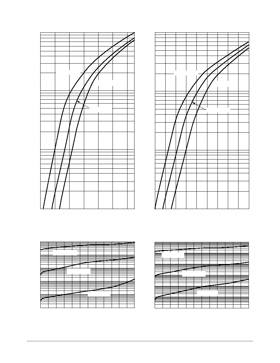
Figure 1. Maximum Forward Voltage
V
F
, INTANTANEOUS VOLTAGE (VOLTS)
I
F
, INST
ANT
ANEOUS FOR
W
ARD CURRENT (AMPS)
V
R,
REVERSE VOLTAGE (VOLTS)
I
R,
REVERSE CURRENT (
µ
A)
0
400
300
200
500
100
600
I
r
@ 25
∞
C
V
F
@ 25
∞
C
V
F
@ 100
∞
C
V
F
@ 175
∞
C
I
r
@ 175
∞
C
I
r
@ 100
∞
C
Figure 2. Typical Forward Voltage
V
F
, INSTANTANEOUS FORWARD CURRENT (AMPS)
I
F
, INST
ANT
ANEOUS FOR
W
ARD CURRENT (AMPS)
0.3
1.1
0.9
0.7
0.5
1.3
1.5
1.7
1.9
2.1
100
10
1
0.1
10
Figure 3. Maximum Reverse Current
V
R
, REVERSE VOLTAGE (VOLTS)
I
R
, REVERSE CURRENT (
µ
A)
0
400
500
300
200
600
100
0.1
100
1
1000
10000
Figure 4. Typical Reverse Current
zl
V
F
@ 25
∞
C
V
F
@ 100
∞
C
V
F
@ 175
∞
C
V
F
@ 25
∞
C
V
F
@ 100
∞
C
V
F
@ 175
∞
C

MSR1560
http://onsemi.com
4
20
10
0
30
5
20
100
0
15
50
0
150
T
C
, CASE TEMPERATURE (
∞
C)
I
F(A
V
)
, A
VERAGE FOR
W
ARD
10
I
F(AV)
, AVERAGE FORWARD CURRENT (AMPS)
Figure 5. Current Derating
Figure 6. Power Dissipation
P
F(A
V
)
, A
VERAGE POWER DISSIP
A
TION
(W
A
TTS)
25
200
0
10
20
dc
Square Wave
dc
Square Wave
350
300
250
200
150
100
50
0
400
350
20
300
250
30
10
0
40
V
R
, REVERSE VOLTAGE (VOLTS)
C, CAP
ACIT
ANCE (pF)
200
150
100
50
0
V
R
, REVERSE VOLTAGE (VOLTS)
Figure 7. Maximum Capacitance
Figure 8. Typical Capacitance
C, CAP
ACIT
ANCE (pF)
50
0
40
50
30
20
10
T
J
= 25
∞
C
T
J
= 25
∞
C
60
50
40
30
20
10
0
80
60
40
20
0
Figure 9. Typical Trr vs. di/dt
dI/dt (A/
µ
S)
Figure 10. Typical Trr vs. Temperature
TEMPERATURE (
∞
C)
T
ime (nsec)
T
ime (nsec)
250
175
100
25
75
125
25
175
T
rr
vs. di/dt @ 25
∞
C
t
a
vs. di/dt @ 25
∞
C
t
b
vs. di/dt @ 25
∞
C
t
rr
t
a
t
b
T
J
= 175
∞
C
T
J
= 175
∞
C

MSR1560
http://onsemi.com
5
3
2
1
0
50
40
30
20
Figure 11. Typical Peak Reverse Recovery
Current
dI/dt (A/
µ
S)
Figure 12. Typical Reverse Recovery Charge
dI
F
/dt (A/
µ
S))
I
RRM
, PEAK RECOVER
Y CURRENT
(AMPS)
Q
RR
, REVERSE RECOVER
Y CHARGE (nC)
I
F
= 1 A
25
225
175
125
75
25
250
175
100
35
25
45
55
65
dI
F
/dt (A/
µ
S)
E
OFF
, SWITCHING OFF LOSSES (
µ
J)
Figure 13. Typical Switching Off Losses
25
175
100
250
I
F
= 1 A
I
F
= 1 A
T
J
= 25
∞
C
T
J
= 25
∞
C
V
R
= 30 V