 | –≠–Ľ–Ķ–ļ—ā—Ä–ĺ–Ĺ–Ĺ—č–Ļ –ļ–ĺ–ľ–Ņ–ĺ–Ĺ–Ķ–Ĺ—ā: AN5195K | –°–ļ–į—á–į—ā—Ć:  PDF PDF  ZIP ZIP |
ICs for TV
1
AN5195K-C
Single chip IC for PAL/NTSC color TV
(built-in I
2
C bus interface)
s
Overview
The AN5195K-C is an IC in which all of the
PAL/NTSC system color television signal process-
ing circuits are integrated on one chip. The ratio-
nalization of set production line can be realized by
the incorporation of I
2
C bus interface.
s
Features
∑
Built-in video IF circuit, sound IF circuit, video
signal processing circuit, color signal processing
circuit, and sync. signal processing circuit
∑
Rationalization of set production line can be real-
ized by the incorporation of I
2
C bus interface
∑
Can be applied to PAL/NTSC/AV-NTSC/M-
NTSC system
∑
Package: 64-SDIP, supply voltage: 5 V, 9 V
s
Applications
∑
TV, TV-video combination
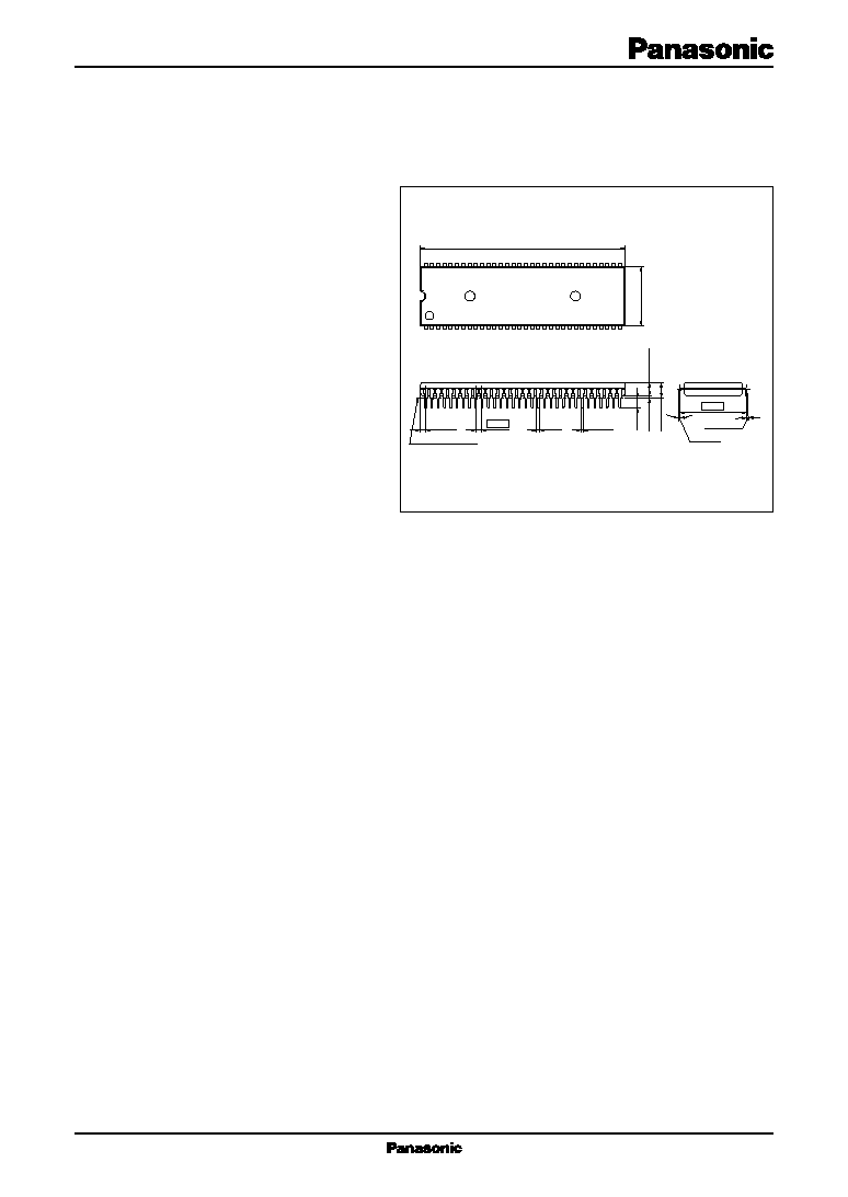
SDIP064-P-0750B
Unit: mm
64
33
1
32
1.778
19.05
0.25
+0.1
≠ 0.05
0.5
+0.1
≠ 0.05
0
į
to 15
į
5.2 max.
0.7 min.
(3.3)
3.85Ī0.2
17.0Ī0.2
(1.0)
(1.641)
Seating plane
58.4Ī0.3

AN5195K-C
ICs for TV
2
s
Block Diagram
1
2
3
4
5
6
7
8
9
10
11
12
13
15
16
17
18
19
20
21
22
23
24
25
26
27
28
29
30
31
32
14
(R) clamp filter
(G) clamp filter
(B) clamp filter
Killer filter
Killer out,50 Hz/60 Hz out
SECAM det. out
APC filter
Chroma VCO (4.43 MHz)
Chroma VCO (3.58 MHz)
BL det.
Y
S
in
R-in
G-in
B-in
R-out
G-out
B-out
Hor. lock det.
GND (RGB/DAC)
ACL
SDA
SCL
V
CC3
(VIF/SIF)
VIF1 in
VIF2 in
GND(VIF/SIF)
RF AGC
Audio out
De-emphasis
AFT out
Ext. video in
Decoupling
V
CC1
(9 V)
64
63
62
61
60
59
58
57
56
55
54
53
52
51
50
49
48
47
46
45
44
43
42
41
40
39
38
37
36
35
34
33
-
(R
-
Y) in
-
(B
-
Y) in
S.C.P
-
(R
-
Y) out
-
(B
-
Y) out
SECAM interface
V-out
Ver. clamp
H-out
X-ray protect
Hor. VCO
AFC1 filter
AFC2 filter
V
CC2
FBP in
GND(VCJ)
C in/black expansion
V
CC3
(VCJ)
Sync. in
Y-in
Video out
VIF VCO
VIF APC1 filter
VIF det. out
Int. video2 in
SIF APC filter
Int. video1 in
IF AGC filter
SIF1 in
SIF2 in
Ext. audio in
SIF3 in/ sharpness
Saturation
Matrix
R
-
Y
demod
+
/
-
B
-
Y
demod
*6-bit
G
-
Y
RGB SW
PN/S
SW
B
clamp
G
clamp
R
clamp
Brightness
Killer
50 Hz/60 Hz
SECAM det SW
Killer
ident
50 Hz /60 Hz detect
CW
generate
Chroma
VCO
AC
C
det.
T
int
APC
Ve
r
.
out
Shut
do
wn
Ve
r
.
count do
wn
AC
C
amp.
*2-bit
(50 Hz
/60 Hz)
*
7-bit
2-bit
1-bit
*6-bit
(*6-bit)
Contrast
R
*Dri
v
e
7-bit *Cut of
f
8-bit
G
*Cut of
f
8-bit
B
*Dri
v
e
7-bit *Cut of
f
8-bit
1H
FF
System
SW
LPF
*1-bit
Hor
.
count
do
wn
BGP
HVBLK
HVCO
Hor
.
re
g.
HBLK
AFC1
AFC2
SCP
Hor
.
lock DET
Ve
r
.
sync. sep.
Hor
.
sync. sep.
Black
e
xpansion
Y
contrast
CV
clamp
Y
clamp
Sharpness
I
2
C b
u
s
interf
ace
SW out
DAC
out
IF
amp.
RF
AG
C
Le
v
e
l
adjust
*6-bit
VIF
detect
Phase
shift
IF
AG
C
AFT
Limiter
APC1
VCO
*3-bit
V
ideo SW *1-bit
*7-bit
SIF
detect
VCO
Pre-amp.
De-
emphasis
LPF
SIF SW
*2-bit
*6-bit
*9-bit
*1-bit
ASW
*1-bit
*1-bit
*3-bit
ICs for TV
AN5195K-C
3
Pin No.
Description
1
(R) clamp
2
(G) clamp
3
(B) clamp
4
Killer filter
5
Killer out, 50 Hz/60 Hz out, SECAM det. out
6
Chroma APC filter
7
Chroma VCO (4.43 MHz)
8
Chroma VCO (3.58 MHz)
9
Black level det.
10
Y
S
input
11
External R input
12
External G input
13
External B input
14
V
CC1
15
R output
16
G output
17
B output
18
Hor. lock detect
19
GND (RGB/I
2
C/DAC)
20
ACL
21
SDA
22
SCL
23
V
CC3-1
(VIF/SIF)
24
VIF1 input
25
VIF2 input
26
GND (VIF/SIF)
27
RF AGC output
28
Audio output
29
De-emphasis
30
AFT output
31
External video input
32
DC decoupling filter
Pin No.
Description
33
SIF3 input/ sharpness
34
External audio input
35
SIF2 input
36
SIF1 input
37
IF AGC filter
38
Internal video1 input
39
SIF APC filter
40
Internal video2 input
41
VIF detect output
42
VIF APC1 filter
43
VIF VCO
(f
P
/2)
44
Video output
45
Y input
46
HV sync. input
47
V
CC3-2
(chroma/jungle/DAC)
48
Chroma input/black expansion start
49
GND (video/chroma/jungle)
50
FBP input
51
V
CC2
(hor. stability supply)
52
AFC2 filter
53
AFC1 filter
54
Hor.
VCO
(32 f
H
)
55
X-ray protection input
56
Hor. pulse output
57
Ver. sync. clamp
58
Ver. pulse output
59
SECAM interface
60
-
(B
-
Y) output
61
-
(R
-
Y) output
62
Sandcastle pulse output
63
-
(B
-
Y) input
64
-
(R
-
Y) input
s
Pin Descriptions
AN5195K-C
ICs for TV
4
Parameter
Symbol
Rating
Unit
Supply voltage
V
CC
V
CC1
(14)
10.5
V
V
CC3
(23, 47)
6.0
Supply current
I
CC
I
14
67
mA
I
23+47
126
I
51
27
Power dissipation
*2
P
D
1,480
mW
Operating ambient temperature
*1
T
opr
-
20 to
+
70
įC
Storage temperature
*1
T
stg
-
55 to
+
150
įC
s
Absolute Maximum Ratings
Note) *1 : Except fot the operating ambient temperature and storage temperature, all ratings are for T
a
=
25
į
C.
*2 : The power dissipation shown is the value for T
a
=
70
į
C.
Parameter
Symbol
Range
Unit
Supply voltage
V
CC1
8.1 to 9.9
V
V
CC3
4.5 to 5.5
Supply current
I
51
10 to 25
mA
s
Recommended Operating Range
Parameter
Symbol
Conditions
Min
Typ
Max
Unit
Power supply
Supply current 1
I
14
Current at V
14
=
9 V
39
48
57
mA
Supply current 2
I
23
Current at V
23
=
5 V
7
10
13
mA
Supply current 3
I
47
Current at V
47
=
5 V
49
63
77
mA
Stabilized power supply voltage
V
51
Voltage at I
51
=
15 mA
5.8
6.5
7.2
V
Stabilized power supply current
I
51
Current at V
51
=
5 V
2
5
7
mA
Stabilized power supply
R
51
DC measurement, gradient
1
5
10
input resistance
at I
51
=
10 mA and 25 mA
VIF circuit
Typical input: f
P
=
38.9 MHz, V
IN
=
90 dB
Ķ
Video detection output (typ.)
V
PO
Modulation m
=
87.5%, data 0B
=
44
1.7
2.1
2.5
V[p-p]
Video detection output (max.)
V
POmax
0B
=
74
1.9
2.6
3.3
V[p-p]
Video detection output (min.)
V
POmin
0B
=
04
1.1
1.6
2.1
V[p-p]
Video detection output f characteristics
f
PC
Frequency to become
-
3 dB for 1 MHz
5.5
8
12
MHz
Sync. peak value voltage
V
SP
Sync. peak voltage at V[p-0] measurement
1.6
2.0
2.4
V
APC pull-in range (H)
f
PPH
High band side pull-in range
1.0
2.0
MHz
(difference from f
P
=
38.9 MHz)
APC pull-in range (L)
f
PPL
Low band side pull-in range
-
2.0
-
1.0
MHz
(difference from f
P
=
38.9 MHz)
RF AGC delay point adjusting
V
RFDP
Delay point (input to become
75
95
dB
Ķ
range
V
27
=
approx. 6.5 V) at data 0A
=
00 to 3F
s
Electrical Characteristics at T
a
=
25
į
C

ICs for TV
AN5195K-C
5
Parameter
Symbol
Conditions
Min
Typ
Max
Unit
VIF circuit (continued)
Typical input: f
P
=
38.9 MHz, V
IN
=
90 dB
Ķ
VCO free-running frequency
f
P
Dispersion without input V
IN
,
-
1.2
0
1.2
MHz
V
37
(IF AGC)
=
0 V(measurement of
difference from 38.9 MHz)
RF AGC maximum sink current
IRF
max
Maximum current IC can sink when pin 27 is low
1.5
3.0
mA
RF AGC minimum sink current
IRF
min
Leakage current of IC, when pin 27 is high
-
50
0
50
Ķ
A
AFT discrimination sensitivity
Ķ
AFT
f
= Ī
25 kHz
40
57
75
mV/kHz
AFT center voltage
V
AFT
V
30
without input V
IN
4.0
4.5
5.0
V
AFT maximum output voltage
V
AFTmax
V
30
at f
=
f
P
-
500 kHz
7.8
8.1
8.7
V
AFT minimum output voltage
V
AFTmin
V
30
at f
=
f
P
+
500 kHz
0.3
0.8
1.0
V
Detection output resistance
R
O41
DC measurement I
O
= -
0.4 mA to
-
1.0 mA
70
120
170
SIF circuit
Typical input: f
S
=
6.0 MHz, f
M
=
400 Hz, V
IN
=
90 dB
Ķ
Audio detection output
V
SOP36
f
= Ī
50 kHz
0.90
1.15
1.40
V[rms]
(PAL, SIF1)
0B
-
D3
=
0
Audio detection output
V
SOP35
f
= Ī
50 kHz
0.90
1.15
1.40
V[rms]
(PAL, SIF2)
0B
-
D3
=
0
Audio detection output
V
SOP33
f
= Ī
50 kHz
0.90
1.15
1.40
V[rms]
(PAL,SIF3)
0B
-
D3
=
0
Audio detection output NTSC/PAL
R
SN/P
f
= Ī
25 kHz, 0B
-
D3
=
1, ratio to PAL (V
SOP36
)
-
2.5
-
0.5
1.5
dB
Audio detection output linearity
V
SOP
Ratio between f
S
=
5.5 MHz
-
3
0
3
dB
and 6.0 MHz, and 6.5 MHz
SIF pull-in range
f
SNH
Pull-in range of high frequency side
4.8
5.0
MHz
NTSC (4.5 MHz)
(4.5 MHz)
SIF pull-in range
f
SNL
Pull-in range of low frequency side
4.0
4.2
MHz
NTSC (4.5 MHz)
(4.5 MHz)
SIF pull-in range
f
SPH
Pull-in range of high frequency side
5.8
6.0
MHz
PAL (5.5 MHz)
(5.5 MHz)
SIF pull-in range
f
SPL
Pull-in range of low frequency side
5.0
5.2
MHz
PAL (5.5 MHz)
(5.5 MHz)
SIF pull-in range
f
SPH
Pull-in range of high frequency side
6.3
6.5
MHz
PAL (6.0 MHz)
(6.0 MHz)
SIF pull-in range
f
SPL
Pull-in range of low frequency side
5.5
5.7
MHz
PAL (6.0 MHz)
(6.0 MHz)
SIF pull-in range
f
SPH
Pull-in range of high frequency side
6.8
7.0
MHz
PAL (6.5 MHz)
(6.5 MHz)
SIF pull-in range
f
SPL
Pull-in range of low frequency side
6.0
6.2
MHz
PAL (6.5 MHz)
(6.5 MHz)
De-emphasis pin
R
29P
Impedance of pin 29 at PAL
32
40
48
k
output resistance (PAL)
De-emphasis pin
R
29N
Impedance of pin 29 at NTSC
48
60
72
k
output resistance (NTSC)
s
Electrical Characteristics at T
a
=
25
į
C (continued)
AN5195K-C
ICs for TV
6
s
Electrical Characteristics at T
a
=
25
į
C (continued)
Parameter
Symbol
Conditions
Min
Typ
Max
Unit
AV SW circuit
Video SW voltage gain
G
VSW
f
=
1MHz, V
IN
=
V[p-p]
5.7
6.7
7.7
dB
Video SW f characteristics
f
VSW
Frequency to become
-
3 dB
8
10
MHz
from f
=
1 MHz, V
IN
=
0.714 V[0-p]
Video SW external input pin voltage
V
31
DC measurement
1.7
2.0
2.3
V
Video SW external output DC voltage
V
44E
DC measurement, 03
-
D7
=
1, 0B
-
D7
=
1
4.2
4.8
5.4
V
Video SW external input resistance
R
I31
DC measurement
44
56
68
k
Video SW output resistance
R
O44
DC measurement, I
O
=
-
0.6 mA to
-
1.0 mA
100
140
180
Video SW internal clamp pin voltage V
38,40
DC measurement, I
IN
=
-
1.0 mA
1.3
1.6
1.9
V
Video SW internal output DC voltage
V
44I
DC measurement
3.7
4.3
4.9
V
Audio SW voltage gain
G
ASW
Data 03
-
D7
=
1, 0B
-
D7
=
1
-
1
0
1
dB
(external input) f
=
400 Hz, V
IN
=
1 V[p-p]
Audio SW input pin voltage
V
34
DC measurement
3.7
4.2
4.7
V
Audio SW output DC voltage
V
28
DC measurement
3.7
4.2
4.7
V
Audio SW input resistance
R
I34
DC measurement
55
65
75
k
Audio SW output resistance
R
O28
DC measurement
200
400
600
Video signal processing circuit
Typical input: 0.6 V[p-p] (V
WB
=
0.42 V[p-p] stair-step), at G-out
Video output (typ.)
V
YO
Data 03
=
20 (typ.) (contrast)
1.9
2.4
2.9
V[0-p]
Video output (max.)
V
YOmax
Data 03
=
3F (max.)
4.1
5.0
5.9
V[0-p]
Video output (min.)
V
YOmin
Data 03
=
00 (min.)
0.15
0.50
1.00
V[0-p]
Contrast variable range
Y
Cmax/min
03
=
3F
15
20
25
dB
03
=
00
Video frequency characteristics
f
YC
Pin 33
=
5 V (sharpness), frequency
5.5
6.0
MHz
to become
-
3 dB from f
=
0.2 MHz
Picture quality variable range
Y
Smax/min
V
33
=
7 V
, f
=
3.8 MHz
9
13
17
dB
V
33
=
5 V
Pedestal level (typ.)
V
PED
Data 02
=
40 (typ.) (brightness)
2.0
2.5
3.0
V
Pedestal level variable width
V
PED
Difference between data 02
=
00 and 7F
2.0
2.6
3.2
V
Brightness control sensitivity
V
BRT
Average amount of change
14
20
26
mV/
at data 02
=
30 and 50 per 1 step
Step
Video input clamp voltage
V
YCLP
Clamp voltage of pin 45
3.2
3.7
4.2
V
ACL sensitivity
ACL
Change of Y-out, when V
20
=
3.0 V
3.5 V
2.4
3.0
3.6
V/V
Blanking off threshold voltage
V
YBL
DC voltage of blanking pulse
1.0
1.5
V
Blanking level
V
STH
Stop voltage of vertical output,
0.3
V
Service SW threshold voltage
*1
when lowering pin 20 (ACL) voltage
DC restoration ratio
T
DC
APL 10% to 90%
90
100
110
%
T
DC
=
AC
-
DC
◊
100
AC
Video input clamp current
I
YCLP
DC measurement: IC inside sink current
8
13
18
Ķ
A
Note) *1: Take great care for not to become V
20
< 0.9 V at set design so that the pin 20 is combined use for service SW when it is used as the ACL.
ICs for TV
AN5195K-C
7
s
Electrical Characteristics at T
a
=
25
į
C (continued)
Parameter
Symbol
Conditions
Min
Typ
Max
Unit
Video signal processing circuit (continued)
Typical input: 0.6 V[p-p] (V
WB
=
0.42 V[p-p] stair-step), at G-out
Pedestal difference voltage
V
IPL
Difference voltage of R,G,B-out pedestal
-
0.2
0
0.2
V
Brightness voltage tracking
T
BL
R,G,B-out fluctuation level ratio of
0.9
1.0
1.1
Times
data 02 (brightness)
=
20 to 60
Video voltage gain relative ratio
G
YC
Output ratio of R,B-out against G-out
0.8
1.0
1.2
Times
Video voltage gain tracking
T
CONT
Gain ratio of R,G,B-out at data 03
0.9
1.0
1.1
Times/
(contrast)
=
10 to 30
Times
Chroma signal processing circuit
Burst 150 mV[p-p] (PAL), reference is B-out
Color-difference output (typ.)
V
CO
Input: Color bar data
2.9
3.7
4.5
V[p-p]
00
=
20 (typ.), 03
=
20 (typ.)
Color-difference output (max.)
V
COmax
Data 00
=
3F, amplitude of one side, 03
=
20
2.6
3.3
V[0-p]
Color-difference output (min.)
V
COmin
Data 00
=
00, 03
=
20
100
mV[p-p]
Contrast variable range
C
Cmax/min
03
=
3F
, 00
=
20
15
20
25
dB
03
=
00
ACC characteristics 1
ACC1
Burst 150 mV[p-p]
300 mV[p-p]
0.9
1.0
1.2
Times
ACC characteristics 2
ACC2
Burst 150 mV[p-p]
30 mV[p-p]
0.8
1.0
1.2
Times
NTSC tint center
C
Difference from data 01
=
20 (tint),
-
7
0
7
Step
when adjusted at tint center
NTSC tint variable range 1
1
Input: Rainbow, data 01
=
3F
30
50
65
deg
NTSC tint variable range 2
2
Input: Rainbow, data 01
=
00
-
65
-
50
-
30
deg
Color-difference output ratio (R)
R/B
Input: Rainbow for both PAL/NTSC
0.46
0.56
0.66
Times
Color-difference output ratio (G)
G/B
Input: Rainbow for both PAL/NTSC
0.28
0.34
0.40
Times
Color-difference output angle (R)
R
Input: Rainbow for both PAL/NTSC
78
90
102
deg
Color-difference output angle (G)
G
Input: Rainbow for both PAL/NTSC
224
236
248
deg
PAL color killer tolerance
V
KILLP
0 dB
=
150 mV[p-p]
-
57
-
44
-
34
dB
NTSC color killer tolerance
V
KILLN
0 dB
=
150 mV[p-p]
-
57
-
44
-
34
dB
APC pull-in range (H)
f
CPH
For both PAL/NTSC
450
700
Hz
APC pull-in range (L)
f
CPL
For both PAL/NTSC
-
700
-
450
Hz
Color killer detection
V
KC
V
5
, when chroma input
4.5
5.0
V
output voltage (color)
Data 0A
-
D6
=
0, 0A
-
D7
=
1, killer out
Color killer detection
V
KBW
V
5
, when chroma input
0
0.1
0.5
V
output voltage (B&W)
Data 0A
-
D6
=
0, 0A
-
D7
=
1, killer out
Demodulation output
-
(B
-
Y)
V
DB
Input: Measurement at pin 60
555
695
835
mV[p-p]
for both color bar PAL/NTSC
Demodulation output
-
(R
-
Y)
V
DR
Input: Measurement at pin 61
430
540
650
mV[p-p]
for both color bar PAL/NTSC
Demodulation output angle
(B
-
Y)
R
DB
Phase shift of B
-
Y axis
-
6
0
6
deg
Demodulation output angle
(R
-
Y)
R
DR
Phase difference from B
-
Y axis
84
90
96
deg
CW output level (4.43 MHz)
V
CWP
AC component, when V
CO
is set at 4.43 MHz
250
350
450
mV[p-p]

AN5195K-C
ICs for TV
8
Parameter
Symbol
Conditions
Min
Typ
Max
Unit
Chroma signal processing circuit (continued)
Burst 150 mV[p-p] (PAL), reference is B-out
CW output level (3.58 MHz)
V
CWN
AC component, when V
CO
is set at 3.58 MHz
50
mV[p-p]
CW output level period (SECAM)
T
CW
CW output period at SECAM and PAL
1.31
1.41
1.51
ms
SECAM discrimination current
I
SECAM
Minimum value for taking out current
50
100
150
Ķ
A
from pin 59 and discriminating as SECAM
SECAM discrimination output
V
SE
V
5
data, when SECAM signal inputted
4.5
5.0
V
0A
-
D6
=
1, 0A
-
D7
=
0, SECAM det. out
PAL/NTSC DC level
V
59PN
V
59
DC level at PAL/NTSC
0.8
1.3
1.65
V
SECAM DC level
V
59S
V
59
DC level at SECAM
4.1
4.6
5.1
V
RGB processing circuit
DAC data are typical
Drive adjustment range
G
DV
AC change amount of R, B-out,
5
6
7
dB
when drive adjustment max. and min.
Cut-off adjustment range
V
CUTOFF
DC change amount of R,G,B-out,
2.1
2.4
2.7
V
when cutoff adjustment max. and min.
Y
S
threshold voltage
V
YSON
Minimum DC voltage, when Y
S
turns on
1.0
V
Y
S
threshold voltage
V
YSOFF
Maximum DC voltage, when Y
S
turns off
0.4
V
External RGB pedestal difference voltage
V
EPL
Y
S
=
5 V
-
200
0
200
mV
Internal and external pedestal
V
PL/IE
Internal-external
200
0
200
mV
difference voltage
External RGB output voltage
V
ERGB
Input 0.7 V[p-p], contrast 03
=
20 (typ.)
1.8
2.2
2.7
V[p-p]
External RGB output difference voltage
V
ERGB
Output ratio of external R,G,B-out
0.8
1.0
1.2
Times
External RGB contrast variable E
Cmax/min
03
=
3F
12
17
22
dB
range
03
=
00
External RGB frequency characteristics f
RGBC
Input 0.2 V[p-p]
8
10
MHz
Internal and external RGB
V
E/I
External 0.7 V[p-p]/internal 0.6 V[p-p]
0.78
0.92
1.06
Times
output voltage ratio
input, contrast 03
=
20 (typ.)
Synchronizing signal processing circuit
Horizontal free-running
f
HO
Without sync. signal input
15.33 15.63 15.93
kHz
oscillation frequency
Horizontal output pulse duty cycle
HO
Upward going pulse duty cycle
31
37
43
%
Horizontal pull-in range
f
HP
Difference from f
H
=
15.625 kHz
Ī
500
Ī
650
Hz
PAL vertical free-running
f
VO-P
Data 01
-
D7
=
1, 02
-
D7
=
0
48
50
52
Hz
oscillation frequency
Forced 50 Hz mode, no sync. signal input
NTSC vertical free-running
f
VO-N
Data 01
-
D7
=
1, 02
-
D7
=
1
58
60
62
Hz
oscillation frequency
Forced 60 Hz mode, no sync. signal input
Vertical output pulse width
VO
For both PAL/NTSC
9
10
11
1/fH
PAL vertical pull-in range
f
VP-P
f
H
=
15.625 kHz, forced 50 Hz mode
46
54
Hz
NTSC vertical pull-in range
f
VP-N
f
H
=
15.75 kHz, forced 60 Hz mode
56
64
Hz
Horizontal output voltage (H)
V
56H
High-level DC voltage
2.9
3.2
3.5
V
Horizontal output voltage (L)
V
56L
Low-level DC voltage
0.3
V
s
Electrical Characteristics at T
a
=
25
į
C (continued)
ICs for TV
AN5195K-C
9
Parameter
Symbol
Conditions
Min
Typ
Max
Unit
VIF circuit
Typical input: f
P
=
38.9 MHz, V
IN
=
90 dB
Ķ
Input sensitivity
V
PS
Input level to become V
PO1
=
-
3 dB
45
dB
Ķ
Maximum allowable input
V
Pmax
Input level to become V
PO1
=
+
1 dB
110
dB
Ķ
SN ratio
SN
P
50
dB
Differential gain
DG
P
5
%
Differential phase
DP
P
5
deg
Black noise detection level
V
BN
Deference from sync. peak value
-
45
IRE
Black noise clamp level
V
BNC
Deference from sync. peak value
45
IRE
RF AGC operation sensitivity
G
RF
Input level difference to become
0.5
3.0
dB
V
27
=
1 V
7 V
VCO switch on drift
f
PD
Frequency drift from 5 seconds
200
kHz
to 5 mins. after SW on
Intermodulation
IM
V
fC
-
V
fP
=
-
2 dB, V
fC
-
V
fP
=
-
12 dB
46
dB
RF AGC adjustment sensitivity
S
RF
Average amount of change of
2
5
V/
output voltage V
27
at data 1 step
Step
Parameter
Symbol
Conditions
Min
Typ
Max
Unit
Synchronizing signal processing circuit (continued)
Vertical output voltage (H)
V
58H
High-level DC voltage
3.9
4.2
4.5
V
Vertical output voltage (L)
V
58L
Low-level DC voltage
0.3
V
Picture center variable range
T
HC
Change amount of phase difference of H
2.6
3.2
4.4
Ķ
s
sync. and H-out of data 0B
=
40 to 47
Overvoltage protective
V
XRAY
Minimum voltage of pin 55
0.60
0.68
0.76
V
operation voltage
at which H-out stops to appear
Vertical frequency
f
50
Vertical frequency to become
47
55
Hz
discrimination 50
V
5
=
low (
<
0.5 V)
Vertical frequency
f
60
Vertical frequency to become
57
63
Hz
discrimination 60
V
5
=
high (
>
4.5 V)
Sync. signal clamp voltage
V
46
V
46
clamp voltage
1.0
1.3
1.6
V
Horizontal output start voltage
V
fHS
Minimum V
50
to become f
0
>
10 kHz,
3.4
4.2
5.0
V
when horizontal oscillation output is
more than 1 V[p-p]
I
2
C interface
Sink current at ACK
I
ACK
Maximum value of pin 21 sink current
1.8
2.5
5.0
mA
when ACK
SCL, SDA signal input high-level
V
IHI
3.1
V
SCL, SDA signal input low-level
V
ILO
0.9
V
Maximum frequency allowable to input
f
Imax
100
kbit/s
∑
Design reference data
Note) The characteristics listed below are theoretical values based on the IC design and are not guaranteed.
s
Electrical Characteristics at T
a
=
25
į
C (continued)
AN5195K-C
ICs for TV
10
Parameter
Symbol
Conditions
Min
Typ
Max
Unit
VIF circuit (continued)
Typical input: f
P
=
38.9 MHz, V
IN
=
90 dB
Ķ
AFT offset adjustment sensitivity
S
AFT
Average amount of change of
0.1
0.3
V/
output voltage V
30
at data 1 step
Step
Video detection output
V
P/V
V
CC
=
Ī
10%
Ī
15
%
fluctuation with V
CC
Video detection output-
V
P/T
T
a
=
-
20
į
C to
+
70
į
C
Ī
10
%
temperature characteristics
Input resistance (pin 24, pin 25)
R
I24,25
f
=
38.9 MHz
1.2
k
Input capacitance (pin24, pin 25)
C
I24,25
f
=
38.9 MHz
4.0
pF
Sound IF output level
V
SIF
f
S
=
38.9 MHz
-
6.0 MHz, P/S
=
20 dB
90
110
dB
Ķ
VCO control sensitivity
P
V
42
=
Ī
0.1 V
2.0
3.5
kHz/mV
VCO control range
f
VCO
Free-running frequency change width
3
5
MHz
at data 0C
=
00 to 7F
RF AGC delay-point temperature
V
DP/T
T
a
=
-
20
į
C to
+
70
į
C
5
dB
characteristics
VCO free-running frequency
f
P/T
T
a
=
-
20
į
C to
+
70
į
C
300
kHz
temperature characteristics
AFT center frequency
f
AFT/T
T
a
=
-
20
į
C to
+
70
į
C, input frequency
300
kHz
temperature characteristics
at which AFT output voltage becomes 4.5 V
External mode output DC
V
41EXT
Output DC voltage at AV SW
0.5
1.0
1.8
V
voltage
external mode
SIF circuit
Typical input: f
S
=
6.0 MHz, f
M
=
400 Hz, V
IN
=
90 dB
Ķ
Input limiting level
V
LIM
Input level to become V
SOP
=
-
3 dB
50
dB
Ķ
AM rejection ratio
AMR
AM
=
30%
55
dB
Total harmonic distortion
THD
f
=
Ī
50 kHz
1.0
%
SN ratio
SN
A
f
=
Ī
50 kHz, f
M
=
400 Hz, on/off
55
dB
Audio output with V
CC
fluctuation
V
S/V
V
CC
=
Ī
10%
Ī
10
%
Audio output temperature
V
S/T
T
a
=
-
20
į
C to
+
70
į
C
Ī
10
%
characteristics
SIF input resistance
R
I35
DC measurement
30
k
SIF input resistance
R
I36
DC measurement
30
k
AV SW circuit
Video SW
CT
VII
f
=
1 MHz, V
IN
=
1 V[p-p]
-
55
dB
cross-talk (Internal
Internal )
Internal
Internal
Video SW
CT
VEI
f
=
1 MHz, V
IN
=
1 V[p-p]
-
55
dB
cross-talk (External
Internal)
Internal
External, External
Internal
Audio SW
CT
AII
f
S
=
6.5 MHz, f
M
=
400 Hz, V
IN
=
1 V[p-p]
-
60
dB
cross-talk (Internal
Internal)
f
S
=
6.5 MHz, f
M
=
1.0 kHz, V
IN
=
1 V[p-p]
s
Electrical Characteristics at T
a
=
25
į
C (continued)
∑
Design reference data (continued)
Note) The characteristics listed below are theoretical values based on the IC design and are not guaranteed.
ICs for TV
AN5195K-C
11
Parameter
Symbol
Conditions
Min
Typ
Max
Unit
AV SW circuit (continued)
SIF SW
CT
AEI
f
S
=
6.5 MHz, f
M
=
400 Hz, V
IN
=
1 V[p-p]
-
60
dB
cross-talk (External
Internal)
Inside f
=
400 Hz, V
IN
=
1 V[p-p]
Video signal processing circuit
Typical input: 0.6 V[p-p] (V
BW
=
0.42 V[0-p] stair-step) at G-out
Black level extension 1
V
BL1
Input: Total black, difference between the
-
100
0
100
mV
voltage at pin 9
=
9 V and open (with RC filter)
Black level extension 2
V
BL2
Input: Total black, difference between
400
700
1 000
mV
the voltage at pin 9
=
3 V and 9 V
Black level extension 3
V
BL3
Input: approx. 20IRE, difference between
100
300
500
mV
the voltage at pin 9
=
open and 9 V,
03 (contrast)
=
3F (max.)
Contrast variation
V
CS
Y-out output level difference,
-
300
0
300
mV
with sharpness
when sharpness max. and min.
Brightness variation
V
BS
Pedestal level DC difference,
-
250
0
250
mV
with sharpness
when sharpness max. and min.
Input dynamic range
V
Imax
03 (contrast)
=
20 (typ.)
1.6
V[p-p]
Y signal SN ratio
SN
Y
03 (contrast)
=
3F (max.)
53
dB
Black level extension start point
V
BLS
Start point at V
48
=
4.5 V
37
42
47
IRE
Video output with V
CC
fluctuation
V
Y/V
V
CC1
=
9 V (allowance:
Ī
10%)
Ī
15
%
Video output-temperature
V
Y/T
T
a
=
-
20
į
C to
+
70
į
C
Ī
10
%
characteristics
ACL start point
V
ACL
V
20
at which output amplitude becomes
3.4
3.7
4.0
V
90% when ACL pin (V
20
) is dereased
from 5 V
Color signal processing circuit
Burst 150 mV[p-p] (PAL), reference is B-out
Demodulation output residual carrier V
CAR1
2 f
SC
level of pin 60 and pin 61
30
mV
Color difference output residual carrier V
CAR2
2 f
SC
level of pin 15, pin 16, and pin 17
50
mV
VCO free-running frequency (PAL)
f
CP
Difference from f
=
4.433619 MHz
-
300
300
Hz
VCO free-running frequency (NTSC)
f
CN
Difference from f
=
3.579545 MHz
-
300
300
Hz
f
CO
fluctuation with V
CC
f
C
/V
CC
V
CC1
=
9 V (allowance:
Ī
10%),
-
300
300
Hz
V
CC3
=
5 V (allowance:
Ī
10%)
Static phase error (PAL)
P
Tint shift, when
f
C
= -
300 Hz to
5
deg/
+
300 Hz change
100 Hz
Static phase error (NTSC)
N
Tint shift, when
f
C
= -
300 Hz to
5
deg/
+
300 Hz change
100 Hz
PAL/NTSC
R
P/N
Output amplitude ratio between PAL and NTSC
0.7
1.0
1.3
Times
Line crawling
V
PAL
Pin 61: Output amplitude difference
50
mV
per 1H for
-
(R
-
Y) pin
Color difference output bandwidth
f
CC
Band to become
-
3 dB
1.0
MHz
s
Electrical Characteristics at T
a
=
25
į
C (continued)
∑
Design reference data (continued)
Note) The characteristics listed below are theoretical values based on the IC design and are not guaranteed.

AN5195K-C
ICs for TV
12
Parameter
Symbol
Conditions
Min
Typ
Max
Unit
Color signal processing circuit (continued)
Burst 150 mV[p-p] (PAL), reference is B-out
Color-difference output
V
C/V
V
CC1
=
9 V (allowance:
Ī
10%),
Ī
15
%
fluctuation with V
CC
V
CC3
=
5 V (allowance:
Ī
10%)
Color-difference output
V
C/T
T
a
= -
20
į
C to
+
70
į
C
Ī
15
%
temperature characteristics
PAL/NTSC output impedance
R
O60,61PN
DC measurement
390
480
570
SECAM output impedance
R
O60,61S
DC measurement
100
k
Color/B&W DC difference
V
CBW
Pedestal level DC difference,
-
60
0
60
mV
voltage
when burst signal with or without
(C
-
Y)/Y
R
C/Y
Color bar input, B-out
0.9
1.2
1.5
V[0-p]/
Contrast typ., color data 00
=
30
V[0-p]
RGB processing circuit
Y
S
changeover speed
f
YS
f
YS
, when Y
S
input is 3 V[0-p],
7
MHz
output level
-
3 dB
External RGB input dynamic range
V
DEXT
Contrast max., data 03
=
3F
1.0
V[p-p]
Internal/external crosstalk
CT
RGB
Leakage, when f
=
1 MHz, 1 V[p-p], Y
S
=
5 V
-
50
dB
Synchronizing signal processing circuit
Lock detection output voltage
V
LD
V
18
, when horizontal AFC lock
5.7
6.3
6.9
V
Lock detection charge
I
LD
DC measurement
Ī
0.6
Ī
0.8
Ī
1.1
mA
and discharge current
EBP (RGB) slice level
V
FBP
Minimum voltage of pin 50, when
0.4
0.75
1.1
V
blanking is applied to RGB output
EBP (AFC2) slice level
V
FBPH
Minimum voltage of pin 50 at which
1.5
1.9
2.3
V
AFC2 operates
Horizontal AFC
Ķ
Ķ
H
DC measurement
30
37
44
Ķ
A/
Ķ
s
Horizontal VCO
H
curve gradient near f
=
15.75 kHz
1.4
1.9
2.4
Hz/mV
Burst gate pulse position
P
BGP
For both PAL/NTSC,
0.2
0.4
0.6
Ķ
s
delay from H. sync. rise
PAL burst gate pulse width
W
BGPP
3.4
4.0
4.6
Ķ
s
NTSC burst gate pulse width
W
BGPN
2.5
3.0
3.5
Ķ
s
Burst gate pulse output voltage
V
BGP
DC voltage of pin 62 in BGP period
4.5
4.7
4.9
V
H blanking pulse output voltage
V
HBLK
DC voltage in H-blanking pulse period
2.1
2.4
2.7
V
of pin 62
V blanking pulse output voltage
V
VBLK
DC voltage in V-blanking pulse period
2.1
2.4
2.7
V
of pin 62
PAL V blanking pulse width
W
VP
Pulse width at f
=
15.625 kHz
1.31
1.41
1.51
ms
NTSC blanking pulse width
W
VN
Pulse width at f
=
15.75 kHz
1.01
1.11
1.21
ms
FBP allowable range
T
FBP
Time from H-out rise to FBP center
12
19
Ķ
s
s
Electrical Characteristics at T
a
=
25
į
C (continued)
∑
Design reference data (continued)
Note) The characteristics listed below are theoretical values based on the IC design and are not guaranteed.

ICs for TV
AN5195K-C
13
Parameter
Symbol
Conditions
Min
Typ
Max
Unit
Synchronizing signal processing circuit (continued)
FBP max. allowable input voltage V
AFBP
2.5
5.0
V
I
2
C Interface
Bus free before start
t
BUF
4.0
Ķ
s
Start condition set-up time
t
SU,STA
4.0
Ķ
s
Start condition hold time
t
HD,STA
4.0
Ķ
s
Low period SCL, SDA
t
LOW
4.0
Ķ
s
High period SCL
t
HIGH
4.0
Ķ
s
Rise time SCL, SDA
t
r
1.0
Ķ
s
Fall time SCL, SDA
t
f
0.35
Ķ
s
Data set-up time (write)
t
SU, DAT
0.25
Ķ
s
Data hold time (write)
t
HD, DAT
0
Ķ
s
Acknowledge set-up time
t
SU, ACK
3.5
Ķ
s
Acknowledge hold time
t
HD, ACK
0
Ķ
s
Stop condition set-up time
t
SU,STO
4.0
Ķ
s
DAC
3, 6, 7-bit DAC DNLE
L
3,6,7
1LSB
=
{data (max.)
-
data (00)}/
0.1
1.0
1.9
LSB
7, 63, 127
Step
8-bit DAC DNLE
L
8
1LSB
=
{data (FF)
-
data (00)}/255
0.1
1.0
1.9
LSB
(except 7F
80)
Step
8-bit DAC DNLE 80
L
8-80
LSB
=
{data (FF)
-
data (00)}/255
0.1
1.0
2.9
LSB
(7F
80)
Step
AFT DAC overlap
Step
Overlap of AFT 8-bit 2-stage
27
32
37
Step
changeover
s
Electrical Characteristics at T
a
=
25
į
C (continued)
∑
Design reference data (continued)
Note) The characteristics listed below are theoretical values based on the IC design and are not guaranteed.
∑
Typical conditions when testing
1. Input signal
1) VIF: f
P
=
38.9 MHz, V
IN
=
90 dB
Ķ
Video modulation : modulated signal is 10-staircase. Modulation m
=
87.5%
V
IN
=
90 dB
Ķ
, pin 25 input level approx. 84 dB
Ķ
2) SIF: f
S
=
6.0 MHz, V
IN
=
90 dB
Ķ
, modulated signal f
M
=
400 MHz, deviation: PAL
Ī
50 kHz, NTSC
Ī
25 kHz
3) Video: 10-stair-step 0.6 V[p-p] (V
BW
=
0.42 V[0-p])
4) Chroma: Color bar signal: Burst level 150 mV[p-p]
Rainbow signal: Burst level 150 mV[p-p]
5) Sync. signal: 0.6 V[p-p]

AN5195K-C
ICs for TV
14
Pin No.
Equivalent circuit
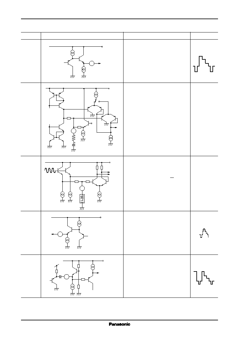
Description
DC (V)
1
Pin 1: Primary color signal clamp pin (R):
DC
2
Pin 2: Primary color signal clamp pin (G):
approx. 7 V
3
Pin 3: Primary color signal clamp pin (B):
∑ Clamp pulse uses internal clamp
pulse (BGP)
4
Killer filter pin:
DC
∑ Filter pin for killer detection circuit
approx. 3.3 V
(operates for BGP period)
∑ Killer turns on (without color out-
put) at 2.8 V or less
s
Terminal Equivalent Circuits
s
Electrical Characteristics (continued)
∑
Typical conditions when testing (continued)
2. I
2
C bus conditions: (PAL)
DAC typical condition
Sub Address
Data (H)
00
20
01
20
02
40
03
20
04
00
05
00
06
00
07
40
08
40
09
01
0A
20
0B
44
0C
C0
Color
Center
Tint
Center
Brightness
Center
Contrast
Center
Cut-off R
Minimum
Cut-off G
Minimum
Cut-off B
Minimum
Drive R, B
Center
Video output
Center
Picture center position
Center
AFT
Center
RF AGC
Center
VIF VCO
Center
SW typical condition
PAL mode
RF being inputted state (Video1 in, SIF1 in)
150
Ķ
A
300
300
9 V
(V
CC1
)
0.01
Ķ
F
Brightness
control
C
BGP
Pins 1,2,3
5 V
(V
CC3
)
Killer
det.
circuit
BGP
4
270
137 k
2.5 V 1.0 M
100
Ķ
A
3.3 V
0.47
Ķ
F
1V
9 V
2.8 V

ICs for TV
AN5195K-C
15
Pin No.
Equivalent circuit
Description
DC (V)
5
Killer, 50 Hz/60 Hz and SECAM det.
DC
output pin:
low-level
∑ Output selecting by SW (I
2
C bus)
0.2 V
∑ Connect 33 k
load resistor of
high-level
pin 5 to microcomputer V
CC
5 V
6
Pin for APC filter:
DC
∑ Filter pin for APC detection circuit
approx. 2.5 V
(operates for BGP period)
∑ Detection sensitivity becomes large
when external R
large (Tends to
pull-in easily. Tends to be affected
by noise)
∑ At SECAM, APC circuit is stopped
by short circuiting 40 k
resistor
7
Pin 7: Chroma oscillation pin (4.43 MHz):
AC
8
Pin 8: Chroma oscillation pin (3.58 MHz):
f
=
f
C
∑ Oscillation pin for chroma. Either
approx. 0.7 V[p-p]
one of 4.43 MHz or 3.58 MHz is
oscillated
∑ Oscillation frequency changeover is
performed by 08
-
D7 bit of I
2
C bus
∑ At 08
-
D7
=
0
I
P1
and I
P2
turn-on and at 4.43 MHz,
oscillation starts
At 08
-
D7
=
1
I
N1
and I
N2
turn-on and at 3.58
MHz, oscillation starts
∑ Pattern design of pin and oscillator
element should be as short as possi-
ble.
s
Terminal Equivalent Circuits (continued)
5
On
Off
10 k
175
Floating
resistor
0.47
Ķ
F
33 k
To
microcomputer
V
CC
for microcomputer
(5 V)
40
Ķ
A
5 V
(V
CC3
)
APC
det.
circuit
BGP
6
270
40
k
SW
2.5 V
R
7.5 k
3.3 V
0.047
Ķ
F
2.2
Ķ
F
1 V
VCO
circuit
max. 1 mA
curve
f
C
V
6
500
Ķ
A
500
Ķ
A
100
Ķ
A
100
Ķ
A
7
8
100
Ķ
A
DC 2.7 V
4.43 MHz
DC 2.7V
3.58 MHz
C7
12 pF
C8
15 pF
I
P1
I
P2
I
N2
I
N1

AN5195K-C
ICs for TV
16
Pin No.
Equivalent circuit
Description
DC (V)
9
Black level detection pin:
DC
Blanking off SW pin
approx. 5.1 V
∑ Black level detection filter pin for
black extension circuit
∑ Holds the most black Y level except
blanking period
∑ Changes operating sensitivity (area
judged as black) of black extension
by external R
Responds with small area when R
goes large.
∑ To stop the black extension, set pin
9 to V
CC
(9 V).
∑ Connected to GND, blanking comes
off. (also the black extension is off)
10
Y
S
input pin:
AC
∑ Fast blanking pulse input pin for
(Pulse)
external analog RGB
∑ Turns on at a voltage of 1 V[0-p] or
more and off at 0.4 V[0-p] or less.
11
Pin 11: External R input pin:
AC
12
Pin 12: External G input pin:
13
Pin 13: External B input pin:
∑ Output changes linearly according
to input level.
14
V
CC1
(typ. 9 V):
DC
∑ Output part of VIF and SIF circuit
9 V
∑ AV SW circuit
∑ Video circuit
∑ RGB circuit
15
Pin 15: R-out pin:
AC
16
Pin 16: G-out pin:
17
Pin 17: B-out pin:
∑ BLK level: Approx. 0.9 V
∑ Black (pedestal) level: Approx. 2.2 V
∑ Blanking can be released when pin 9
(black level detection pin) is set at 0 V.
s
Terminal Equivalent Circuits (continued)
2.7 k
10
9 V
(V
CC1
)
30 k
0.7 V
100
Ķ
A
50
Ķ
A
From
microcomputer
To RGB output
circuit
9
R
180 k
80 k
75 k
5 V
(V
CC3
)
9 V
(V
CC1
)
10 k
To blanking
circuit
To black
expansion circuit
4.7
Ķ
F
80
Ķ
A
100
Ķ
A
5.1 V
10 k
-
Y
9 V
(V
CC1
)
100
Ķ
A
BGP
Pins 11,12,13
To
color
circuit
200
Ķ
A
9 V
(V
CC1
)
100
Ķ
A
C out
500
Ķ
A
50
Pins 15
16
17
100

ICs for TV
AN5195K-C
17
Pin No.
Equivalent circuit
Description
DC (V)
18
Horizontal sync. detection pin:
DC
∑ Phase of horizontal synchronizing
at synchronous
signal and horizontal output pulse is
approx. 6 V
detected and outputted.
at asynchronous
∑ Pin 18 is low at out of phase.
approx. 0.3 V
∑ In asynchronous state, color control
becomes min. and chroma output
disappears.
∑ Pay attention to impedance when
voltage of pin18 is used by micro-
computer (Z
O
500 k
is required)
∑ HV
SYNC
period
When pin 56 is high: I
1
on
When pin 56 is low: I
2
on
19
GND:
∑ RGB circuit
∑ DAC I
2
C circuit
20
ACL pin:
DC
∑ Contrast can be reduced when DC
approx. 3 V
voltage of pin 20 is decreased from
the outside.
∑ Service SW
Note) When pin 20 is used as ACL, set
design must be done not to become
V
20
<
0.9 V so that pin 20 operates
also as the service SW.
21
I
2
C bus data input pin:
AC
(pulse)
s
Terminal Equivalent Circuits (continued)
5 V
(V
CC3
)
6.3 V
(V
CC2
)
10 k
12 k
12 k
18
50
Ķ
A
2.8 V
To
chroma
circuit
I
1
I
2
800
Ķ
A
800
Ķ
A
Z
O
10 k
0.022
Ķ
F
1 M
Pin 56
H-out
Pin 46
HV sync. in
9 V
(V
CC1
)
20
5.9 V
To contrast
circuit
2.1 V
3.5 V
60 k
6.9 k
60 k
2.3 V
2.3 V
Ī
1 V
6.9
k
7.1 k
7.1 k
6.9 k
100
Ķ
A
100
Ķ
A
100
Ķ
A
4.7
Ķ
F
Contrast
control
30 k
30 k
ACK
5 V
(V
CC3
)
21
100 k
50
Ķ
A
100 k
1.7 V
To logic
circuit
From
microcomputer
Data
1 k

AN5195K-C
ICs for TV
18
Pin No.
Equivalent circuit
Description
DC (V)
22
I
2
C clock input pin:
AC
(Pulse)
23
V
CC3-1
(typ. 5 V):
DC
∑ For VIF and SIF circuit
5 V
24
Pin 24: VIF input pin-1:
AC
25
Pin 25: VIF input pin-2:
f
=
f
P
∑ Input for VIF amp. and balanced
DC level
input
approx. 2.7 V
26
GND:
DC
∑ For VIF and SIF circuit
27
RF AGC output pin:
DC
∑ Open collector output. Can be used
at given bias
(max. 12 V)
28
Audio output pin:
AC
0 kHz
to
20 kHz
s
Terminal Equivalent Circuits (continued)
5 V
(V
CC3
)
22
100 k
50
Ķ
A
100 k
1.7 V
To logic
circuit
30 k
30 k
From
microcomputer
Clock
1 k
5 V
(V
CC3
)
25
24
SAW
150
Ķ
A150
Ķ
A
27 k
1.2
k
1.2
k
3.5 V
5 V
(V
CC3
)
RF AGC
control bias
IF AGC
bias
To tuner
40
k
27
9 V
(V
CC1
)
100
Ķ
A 400
Ķ
A
270
28

ICs for TV
AN5195K-C
19
Pin No.
Equivalent circuit
Description
DC (V)
29
De-empahsis pin
AC
∑ De-empahsis filter pin for sound
0 kHz
detection signal.
to
∑ External C is the same for PAL and
20 kHz
NTSC (internal impedance changes)
∑ PAL: 120 k
//60 k
◊
1 200 pF
=
48
Ķ
s
∑ NTSC: 60 k
◊
1 200 pF
=
72
Ķ
s
30
AFT output pin
DC
∑ Center voltage offset should be
adjusted by using bus.
∑ If AFT defeat SW is turned on (09
=
00), V
30
comes to a value determined
by the value of externally attached
resistor dividing.
∑ AFT
Ķ
is variable by impedance of
externally attached resistor.
31
External video input pin
AC
∑ Input pin for external video signal.
1 V[p-p]
DC cut input.
(composite)
∑ Typical 1 V[p-p]
DC
approx. 2.0 V
32
Decoupling pin
DC
∑ S curve inside IC is wide band but
DC feedback is applied so that DC
voltage of output signal becomes
constant.
∑ DC level (typ. 4.5 V)
f
S
high: V
32
low
33
SIF signal input pin
AC
+
DC
∑ Common use with DC input pin for
AC
sharpness control
f
=
f
S
∑ DC bias is applied from external
(DC: 5 V to 7 V for sharpness control)
s
Terminal Equivalent Circuits (continued)
9 V
(V
CC1
)
1.7 k
1 200 pF
29
100
Ķ
A
60 k
120 k
NTSC
PAL
Detection output
9 V
(V
CC1
)
1.1 k
1.1 k
40 k
1.1 k
1.1 k
30
9 V
To tuner
max. 350
Ķ
9 V
(V
CC1
)
31
100
Ķ
A
50 k
30 k
3.4 V
50
Ķ
A
10
Ķ
F
To
video SW
Ext. video
9 V
(V
CC1
)
10 k
32
10
Ķ
F
1.7 k
20 k
1.7 k
13
Ķ
A
100
Ķ
A
3 k
3 k
typ. 4.5 V
9 V
(V
CC1
)
100
Ķ
A
200
Ķ
A
100
Ķ
A
33
4.4 V
30 k
30 k
10 pF
1.8
k
9 V
To SIF
limiter
amp.
Sharpness
contorol
5 V to 7 V
SIF in

AN5195K-C
ICs for TV
20
Pin No.
Equivalent circuit
Description
DC (V)
34
External audio input pin:
AC
∑ Input pin for external audio signal
0 kHz
input. DC cut input.
to
∑ Typical input level should be adjusted
20 kHz
to internal sound level.
35
SIF signal input pin:
AC
+
DC
36
∑ Input pin of SIF1, SIF2 and is biased
AC
in inside.
f
=
f
S
DC
3.0 V
37
IF AGC filter pin:
DC
∑ Pin for IF AGC filter. The current
approx. 2 V
obtained from peak AGC circuit is
smoothed by external capacitor.
∑ Since response becomes faster
when C
small but sag tends to
appear easily.
38
Internal video input pin:
AC
40
∑ Input pin for the signal detected in
1 V[p-p]
the VIF circuit (internal video signal)
(composite)
∑ Input with DC cut
∑ Typical input: 1 V[p-p]
DC level
approx. 1.6 V
39
SIF APC filter pin:
DC
∑ Filter pin of SIF APC circuit
s
Terminal Equivalent Circuits (continued)
9 V
(V
CC1
)
34
150
Ķ
A
65 k
5.4 V
50
Ķ
A
10
Ķ
F
To
audio SW
9 V
(V
CC1
)
200
Ķ
A
100
Ķ
A
3.7 V
30 k
30 k
1.8
k
9 V
To SIF
limiter
amp.
SIF in
40 k
Pins 35
36
100
Ķ
A
5 V
(V
CC3
)
30
Ķ
A
0.47
Ķ
F
37
To
IF amp.
9 V
(V
CC1
)
Int. video
30 k
3.0 V
50
Ķ
A
10
Ķ
F
To
video SW
680 k
Pins 38
40
9 V
(V
CC1
)
72
Ķ
A
200
Ķ
A
5.6
k
13 k
8.4 k
7.5 k
39
VCO
(4 MHz
to 7 MHz)
P.C.
2 pF
1 000 pF
800
Ķ
A
To
audio SW
ICs for TV
AN5195K-C
21
Pin No.
Equivalent circuit
Description
DC (V)
41
VIF detection output pin:
AC
∑ Adjust to 2 V[p-p] by I
2
C bus
2 V[p-p]
(uses upper rank 4-bit of 0 A)
42
APC1 filter pin:
DC
∑ Filter pin of VIF APC1 circuit
approx. 2.5 V
∑ VCO lock detection circuit is incor-
porated in the IC, and it changes
over the time constant of APC filter.
∑ Lock: SW: 0
Unlock: SW: 1
43
VIF oscillation pin:
AC
∑ Chage the oscillation coil according
f
=
f
P
/2
to VIF frequency.
approx. 0.7 V[p-p]
∑ Oscillation frequency is
1
◊
f
P
DC level
2
approx. 3.9 V
44
Video output pin:
AC
∑ Int. video1, int. video2 or ext. video
2 V[p-p]
signal selected by AV SW is outputted.
DC level
approx. 4.5 V
45
Video input pin:
AC
∑ Input pin of video signal (possible
0.6 V[p-p]
also for composite video)
∑ Typical input 0.6 V[p-p]
∑ Sync. top is clamped to 3.5 V
∑ Video signal should be inputted
with low impedance.
s
Terminal Equivalent Circuits (continued)
9 V
(V
CC1
)
75
Ķ
A
41
5 V
(V
CC3
)
42
500
150
50
Ķ
A
SW
1
0
20 k
0.47
Ķ
F
75
Ķ
A
25
Ķ
A
to
VCO
3.25 V
5 V
(V
CC3
)
800
Ķ
A
300
100
43
400
Ķ
A
100
Ķ
A
9 V
(V
CC1
)
50
Ķ
A
44
400
Ķ
A
50
Ķ
A
45
43 k
1.8 k
4.3 V
9 V
(V
CC1
)
47 k
10
Ķ
A
AN5195K-C
ICs for TV
22
Pin No.
Equivalent circuit
Description
DC (V)
46
Vertical and horizontal sync. separation
AC
input pin:
2 V[p-p]
∑ Sync. top is clamped to 1.3 V.
47
V
CC3-2
(typ. 5 V):
DC
∑ Chroma and Jungle circuit use
5 V
48
Chroma signal input pin:
AC
+
DC
Black extension start point adjust-
Burst typ.
ment pin
150 mV[p-p]
∑ Pin 48 is chroma signal input pin
DC typ.
and black extension start point is
4.5 V
adjusted by DC voltage applied
externally.
49
GND:
DC
Video, chroma and jungle circuit use
0 V
50
FBP input:
AC
∑ FBP input pin for horizontal blank-
FBP
ing and APC circuit
∑ Threshold level HBLK: 0.7 V
AFC: 1.9 V
∑ If DC 1.3 V is applied from outside,
the state comes to all blanking
51
Horizontal stabilized power supply pin:
DC
∑ Stabilized power supply for horizon-
6.3 V
tal circuit start up. Zener circuit is in-
cluded inside.
s
Terminal Equivalent Circuits (continued)
5 V
(V
CC3
)
48
100 Ķ
A
25
Ķ
A
9V
(V
CC1
)
To
chroma amp.
50
Ķ
A
15 k
12.5 pF
1 000 pF
10 k
10 k
9 V
Chroma
signal
2.5 V
To
black level
expansion
5 V
(V
CC3
)
16 k
2 V[p-p]
46
To H
sync. sep.
To V
sync. sep.
1.3 V
20
Ķ
A
16 k
C
H
0.1
Ķ
F
270
1 200 pF
R
H
5 V
(V
CC3
)
50 Ķ
A
50 Ķ
A
100 Ķ
A
50
100
Ķ
A
40 k
40 k
To
HBLK
To
AFC
1.9 V
0.7 V
24 k
50 Ķ
A
60 k
51
typ. 15 mA
V
CC2
I
51
47 Ķ
F
To hor. OSC
V
51
6.3 V
I
51
ICs for TV
AN5195K-C
23
Pin No.
Equivalent circuit
Description
DC (V)
52
Horizontal AFC2 filter pin:
DC
∑ Pulse phase of FBP and IC inside are
1.5 V
compared and capacitor connected to
to
pin 52 is charged or discharged.
3.5 V
∑ Screen center position adjustment is
executed by charge or discharge of
DC current with DAC.
∑ According to the time from H-out to
FBP-in, V
52
is changed, and slice
level of inside saw-tooth waveform is
changed.
53
Horizontal AFC1 filter pin:
DC
∑ Pulse phase of horizontal sync. sig-
typ. 4.3 V
nal and IC inside are compared and
capacitor connected to pin 53 is
charged or discharged.
∑ R1, R2, C1 and C2 are lag-lead fil-
ters for AFC1
54
Horizontal oscillation pin:
AC
∑ Oscillation is done at 32
◊
f
H
503 kHz
f
=
32 f
H
by ceramic resonator.
(approx. 503 kHz)
∑ Horizontal and vertical pulse are
made by count-down circuit of IC
inside.
55
Overvoltage protection input pin:
DC
∑ Input pin for protection circuit
Normally 0 V
against X-ray caused by overvoltage.
∑ Shut-down is started by inside logic
circuit when H-out is low. (break-
down protection of horizontal drive
T
R
)
56
Horizontal pulse output pin:
AC
∑ Pulse duty approx. 36%
Pulse
s
Terminal Equivalent Circuits (continued)
6.3 V
(V
CC2
)
AFC2
detecter
52
0.022
Ķ
F
2 k
2 k
1 k
1 k
I
From DAC
(hor. position)
50
Ķ
A
3.3 V
1.9V
To hor. out
V
52
max.500
Ķ
A
6.3 V
(V
CC2
)
200
Ķ
A
Hor.
OSC
AFC1
detecter
53
27 k
R1
27 k
4.3 V
0.033
Ķ
F
C1
820
R
2
22
Ķ
F
C2
1.5 V
1 000
Ķ
A
Hor. sync.
Horizontal
curve
f
H
V
53
6.3 V
(V
CC2
)
54
80
Ķ
A
22 k
10 k
10 k
300
200
Ķ
A
100
Ķ
A
220 pF
6.3 V
(V
CC2
)
40 k
20 k
20 k
55
4.3 V
3 V
20 k
To
count down
6.3 V
(V
CC2
)
56
50
2.8 V
40 k
10 k
0 V
Hor. out
19 k
4.3 V
AN5195K-C
ICs for TV
24
Pin No.
Equivalent circuit
Description
DC (V)
57
Vertical sync. signal clamp pin:
AC
∑ Peak clamp pin in order to separate
f
=
f
V
vertical sync. signal
∑ Integrating amount of vertical sync.
signal itself is determined by time
constant of inside but triggering tim-
ing is determined by selecting R1
and C1 of external time constant.
∑ Uses with R1 > 200 k
∑ R2 is for emitter current limiting resistor
58
Vertical pulse output pin:
AC
∑ Negative polarity, pulse width 10 H
Pulse
59
SECAM interface pin:
AC+DC
∑ Inpu/output pin for interface with
AC
SECAM IC
250 mV[p-p]
∑ SECAM mode is made by taking the
or
curr. of 100
Ķ
A or more from pin 59.
0 mV[p-p]
∑ At SECAM
DC
DC4.4 V
+
AC250 mV[p-p]
4.4 V
∑ At non-SECAM
or
DC1.1 V
+
AC250 mV[p-p]: 4.43 MHz
1.1 V
or
0 mV[p-p]: 3.58 MHz
60
Pin 60:
-
(B
-
Y) output pin:
AC
61
Pin 61:
-
(R
-
Y) output pin:
-
(B
-
Y)
∑ At SECAM, output circuit is off
and comes to high impedance.
∑ Output to 1HDL
-
(R
-
Y)
DC level
approx. 2.1 V
62
Sandcastle pulse output pin:
AC
∑ Sandcastle pulse is outputted to
Pulse
1HDL and SECAM IC.
4.7 V
2.4 V
5 V
(V
CC3
)
57
4 k
16 k
200
R1
330 k
4.3 V
50 k
3 k
C1
0.33
Ķ
F
R2
220
270
To
ver.
count
down
50 k
5 V
(V
CC3
)
43 k
58
4.3 V
0 V
9 V
(V
CC1
)
59
12 k
50
Ķ
A
12 k
50 k
100
Ķ
A
200
Ķ
A
SECAM
SECAM
SECAM
detecter
56.2 k
13.7 k
61.5 k
f
C
To
SECAM IC
5 V
(V
CC3
)
60
6 1
1.5 k
1.5 k
100
Ķ
A
100
Ķ
A
100
Ķ
A
SECAM
SECAM
0 V
2.5 k
-
(B
-
Y)
-
(R
-
Y)
To 1HDL
5 V
(V
CC3
)
62
15 k
37 k
42 k
63 k
44 k
VBLK
HBLK
BGP
s
Terminal Equivalent Circuits (continued)

ICs for TV
AN5195K-C
25
Pin No.
Equivalent circuit
Description
DC (V)
63
Pin 63:
-
(B
-
Y) input pin:
AC
64
Pin 64:
-
(R
-
Y) input pin:
-
(B
-
Y)
∑ Input color difference signal from
1HDL output .
∑ Pedestal level is clamped to 4 V by
-
(R
-
Y)
clamp circuit.
DC level
4 V
s
Terminal Equivalent Circuits (continued)
9 V
(V
CC1
)
100
Ķ
A
CCP
Pins 63,64
200
Ķ
A
To
color
circuit
From
1HDL
s
System Application Example
AN5195K-C (PAL/NTSC)
U/V
tuner
AN5071
Band SW
EEPROM
AN5637
SECAM
decoder
MN3868
1H CCD
delay line
MN152810
MN1871274
System MCU
I
2
C bus
PNA4602M
IR reciever
unit
VIF amp.
Video det.
AN5265
Sound
output
AN5534
Ver. def.
Ver. output
SIF amp.
FM det.
Video/chroma
signal process
2SC3942
Video output
Deflection
signal process
2SC4212
Hor. drv.
2SD2522
Hor. output
CRT
AN5195K-C
ICs for TV
26
s
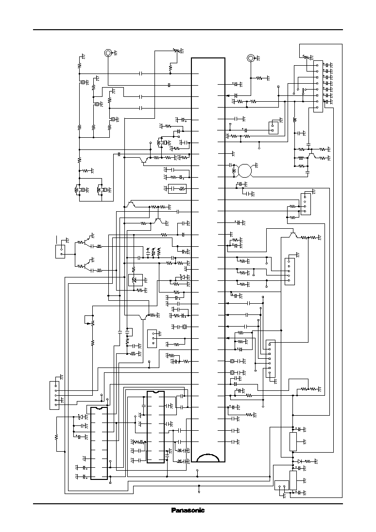
Application Circuit Example
1
2
3
4
5
6
7
8
9
10
11
12
13
15
16
17
18
19
20
21
22
23
24
25
26
27
28
29
30
31
32
14
64
63
62
61
60
59
58
57
56
55
54
53
52
51
50
49
48
47
46
45
44
43
42
41
40
39
38
37
36
35
34
33
9
10
11
12
13
15
16
14
8
7
6
5
4
2
1
3
MN3868(1H DL)
-
(R
-
Y)
-
(B
-
Y)
5 V
9 V
0.1
Ķ
F
82
Ķ
H
0.1
Ķ
F
0.1
Ķ
F
33 pF
82
Ķ
H
33 pF
0.01
Ķ
F
0.01
Ķ
F
In
S.C.P
-
(B
-
Y)
out
-
(R
-
Y) out
0.1
Ķ
F
0.1
Ķ
F
2.2
Ķ
F
680 k
SECAM interface
V out
8.2
Ķ
H
33 pF
0.1
Ķ
F
X-ray protect.
AFC1
AFC2
FBP in
100 pF
120 pF
4.7
Ķ
H
1.2 k
Det. out
Sync. in
2 V[p-p]
9 V
9 V
VOSC
APC1
AGC
1 V[p-p]
GND
HOSC
0.01
Ķ
F
0.047
Ķ
F
0.047
Ķ
F
820
5 V
9
10
11
12
13
15
16
14
8
7
6
5
4
2
1
3
SECAM
AN5195K-C
51
Ver.
clamp
H out
V
ideo out
V
ideo
in
0.22
Ķ
F
0.1
Ķ
F
47
Ķ
F
0.022
Ķ
F
(8 V)
1
2
3
4
5
1
3.58/4.43
On
2
10 k
10 kB
47 pF
2.2 k
3
2
1
220
220 pF
820
180
3.3 k
10 k
C in
10 k
1.8 k
10
Ķ
F
270
910
910
680 k
2 k
1 k
150
1 200 pF
0.47
Ķ
F
1 000 pF
0.47
Ķ
F
10
Ķ
F
Ext. audio
5.1 k
10 kB
0.01
Ķ
F
0.01
Ķ
F
0.01
Ķ
F
Video out
Y in
2.2 k
1.8 k
1 k
30 pF56
Ķ
H
10 k
10
Ķ
F
0.033
Ķ
F
47
Ķ
F
1 000 pF
47
Ķ
F
0.1
Ķ
F
1 200 pF
0.022
Ķ
F
V
CC2
V
CC3
5 V
10 k
(VCJ)
(VCJ)
9 V
T
rap&DL (340 nsec
Ī
35 nsec)
150 pF2.7
Ķ
H
10 k
3.58 MHz T
rap
130 k
680 k
5.5 H
T
rap
12 H
Int. V2
Int.
V1
APC
SIF
SIF1 in
SIF2 in
SIF3 in
sharpness
Ext. audio in
Sharpness
6.5 H
10
Ķ
F
910
470
470
910
6.0 H
BPF
470
470
BPF
470
BPF
470
4.5 MHz
6.5 MHz
5.5 MHz 6.0 MHz
V
CC3
=
5 V
0.022
Ķ
F
33 k
2.2
Ķ
F
0.047
Ķ
F
0.47
Ķ
F
4.7
Ķ
F
180
k
1 M
12 pF
15 pF
1 M
APC
R
0.022
Ķ
F
G
Clamp f
ilter
Killer out 50 Hz/60 Hz out SECAM det. out
Killer
0.022
Ķ
F
0.47
Ķ
F
0.47
Ķ
F
0.47
Ķ
F
0.47
Ķ
F
R
Y
S
B L
det.
B
U-COM
4.43
MHz
3.58
MHz
567
4
3
2
1
G
B
R
47
Ķ
F
1.5 k
G
1.5 k
B
1.5 k
5
V
CC1
(9 V)
Hor
. lock det.
4
3
2
1
0.022
Ķ
F
4.7
Ķ
F
0.01
Ķ
F
0.01
Ķ
F
V
CC3
(VIF/SIF)
GND (RGB/DAC)
ACL
SDA
SCL
1 M
4.7
4.7
1.2
Ķ
H
39 k
150 k
150 k
75
6.8 k
8.2
Ķ
H
0.01
Ķ
F
1 200 pF
10
Ķ
F
910
1 k
7.5 k
56
3.6 k
10 k
1
2
3
4
1
2
0.01
Ķ
F
47
Ķ
F
0.01
Ķ
F
10
Ķ
F
10
Ķ
F
De-emphasis
Decoupling
AFT
SA
W
0.39
Ķ
H
GND
(VIF/SIF)
RF AGC
Aidio out
4
3
1
2
Ext.video
15 k
15 k
10 kB
47
Ķ
F
10
Ķ
F
10
Ķ
F
10
Ķ
F
10
Ķ
F
10
Ķ
F
10
Ķ
F
+
B (12
V)
AG
C
BH
BT
BU
TU1
BL
AFT
BM
1F
SW1
Band SW
AN78M05
47
Ķ
F
47
Ķ
F
100
Ķ
F
V
CC1
=
9 V
AN78M09
1.8 k
1 2