ICs for TV
s
Overview
The AN5790N and AN5792 are the intergrated circuits
designed for CRT display horizontal signal processing cir-
cuits.
s
Features
∑
Horizontal synchronous signal is available in both polar-
ities.
∑
Wide range of horizontal osciallation frequency : 14kHz
to 60kHz.
∑
Output pulse width : 2µs to 40µs
∑
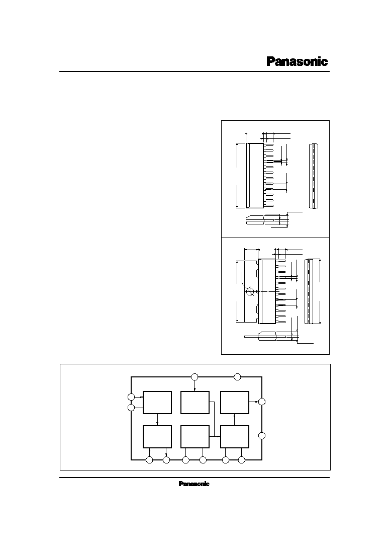
Package
AN5790N...NF-12S(12-Pin SIL plastic package)
AN5792...F-12S (12-Pin SIL plastic package with fin)
AN5790N, AN5792
Horizontal Signal Processing ICs for CRT Display
1
2
3
4
5
6
7
8
9
10
11
12
1.7
±
0.25
2.54
1.2
±
0.25
7.9
±
0.3
3.5
±
0.25
1.2
±
0.25
0.5
±
0.1
0.45
+ 0.1
≠ 0.05
1.7
±
0.25
Unit : mm
29.4
±
0.3
12-Pin SIL Plastic Package (12-SIP)
AN5790N
6
5
8
7
10
9
11
12
4
3
2
1
V
CC
GND
Polarity
Switch
X-ray
Protector
Pre-Amp.
AFC
Hor. Osc.
PulseWidth
Adjustment
s
Block Diagram
1
2
3
4
5
6
7
8
9
10
11
12
¯3.3
1.7
±
0.25
2.54
1.2
±
0.25
5.8
±
0.25
7.9
±
0.3
3.5
±
0.25
1.2
±
0.25
0.5
±
0.1
29.4
±
0.3
0.45
+ 0.1 ≠ 0.05
1.7
±
0.25
28.0
±
0.3
AN5792
12-Pin SIL Plastic Package with Fin (12-SIF (f))
Unit : mm
ICs for TV
AN5790N, AN5792
Parameter
Symbol
Rating
Unit
V
CC
I
CC
P
D
T
opr
T
stg
Power dissipation
Supply current
Supply voltage
Operating ambient temperature
Storage temperature
Temperature
13.2
1140
≠ 20 to +70
≠ 40 to +150
V
mW
∞C
∞C
mA
50
s
Absolute Maximum Ratings
(Ta= 25∞C)
V
2-7
V
2-7
Positive polarity signal input
Negative polarity signal input
Total circuit current
Polarity switching voltage (1)
Polarity switching voltage (2)
0
2.5
0.4
5.5
V
V
Parameter
min
Condition
typ
max
Unit
Symbol
V
OSC-S (H)
f
HO
=12kHz to 19kHz
Horizonal oscillation start voltage
7.5
V
f
HO (1)
V
CC
=11V, C= 4400pF
Horizonal oscillation frequency
15
15.75
16.5
kHz
f
HO (2)
V
CC
=11V, C= 820pF, 5600pF
14
60
kHz
I
tot
V
CC
=11V
30
45
60
mA
f
HO
/V
CC
f
HO
=15.75kHz, f
HO
| 9.9V≠ f
HC
| 12.1V
f
HO
supply voltage dependency
40
130
Hz
f
HO
/Ta
f
HO
=15.75kHz, f
HO
| ≠20∞C ≠ f
HC
| 60∞C
260
Hz
I
O
=
±
25
µ
A
Oscillation frequency control sensitivity
16
17.6
19.3
Hz/
µ
A
f
DC
µ
◊
DC loop gain
700
Hz/
µ
s
HO (1)
V
CC
=11V, R= 20k
, C= 6800pF
Output pulse width
17.8
19.4
21.2
µ
s
HO (2)
V
CC
=11V, R=20k
, C=330pF, 18000pF
Output pulse width
2
40
µ
s
HO
/V
CC
V
CC
= 9.9V to 12.1V
Output pulse width variation to supply voltage change
5
%
HO
/Ta
V
CC
=11V, Ta= ≠ 20∞C to + 60∞C
Output pulse width variation to temeprature change
5
%
V
8-7
V
CC
=11V, V
10-7
=1V
Oscillation output saturation voltage
2
V
I
8-7
V
CC
=11V, V
10-7
=1V
Oscillation output drive current
300
mA
V
6-7
V
CC
=11V
X-ray protecting circuit operation start voltage
0.5
0.64
0.75
V
Horizonal oscillation frequency
f
HO
ambient temperature dependency
s
Electrical Characteristics
(Ta= 25∞C)
s
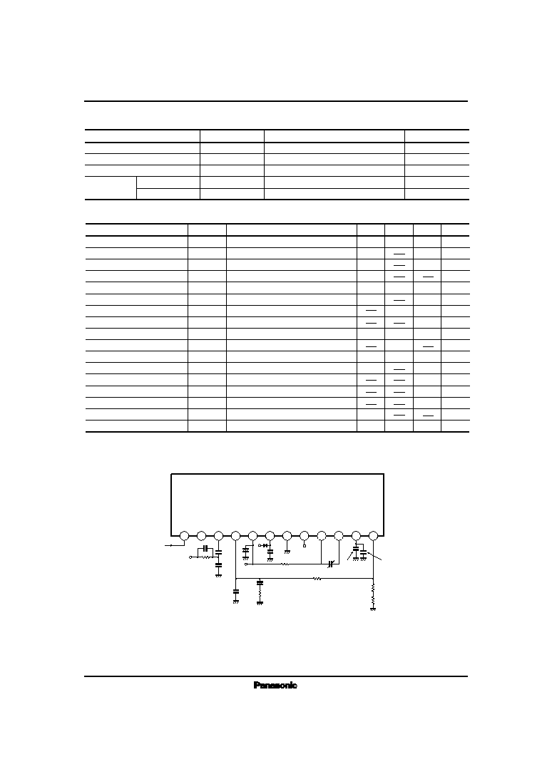
Application Circuit
27k
+
≠
4.7
µ
F
V
CC
(11V)
AN5790N/AN5792
+
≠
+
≠
20k
2k
2.7k
33k
39pF
2700pF
(Styrol Cap.)
2700pF
(Mylar Film Cap.)
Output
Hor. Sync. Signal
FBK Pulse Input
3.3k
0.033
µ
F
0.018
µ
F
0.015
µ
F
220
µ
F/16V
33
µ
F/50V
1
2
3
4
5
6
7
8
9
10
11
12
ICs for TV
AN5790N, AN5792
Horizontal
synchronous
signal input pin
Polarity
discrimination
switching pin
Flyback pulse
input pin
AFC output pin
Supply voltage
X-ray protecting
circuit input pin
Horizontal drive
output pin
Both polarities of an input signal of
Pin1 are made available by connect-
ing this pin to GND or setting it to
OPEN
Flyback feedback pin.
The standard value of amplitude is
1.5Vpp.
Result of AFC detection.
When a voltage of 0.75V or more is
applied, no horizonal output will
not be generated.
Current when turned ON should be
used at 300mA or less.
1
2
3
4
6
8
Pin No.
Pin name
Typ. waveform
Description
Equivalent circuit
5
7
GND
DC
DC
DC
DC
5V
0V
8
6
4
3
2
1
5V
4k
5V
4k
5.9V
200
680
2
DC
Pin for inputting a horizontal syn-
chronous signal.
s
Pin Descriptions

Please read the following notes before using the datasheets
A. These materials are intended as a reference to assist customers with the selection of Panasonic
semiconductor products best suited to their applications.
Due to modification or other reasons, any information contained in this material, such as available
product types, technical data, and so on, is subject to change without notice.
Customers are advised to contact our semiconductor sales office and obtain the latest information
before starting precise technical research and/or purchasing activities.
B. Panasonic is endeavoring to continually improve the quality and reliability of these materials but
there is always the possibility that further rectifications will be required in the future. Therefore,
Panasonic will not assume any liability for any damages arising from any errors etc. that may ap-
pear in this material.
C. These materials are solely intended for a customer's individual use.
Therefore, without the prior written approval of Panasonic, any other use such as reproducing,
selling, or distributing this material to a third party, via the Internet or in any other way, is prohibited.
Request for your special attention and precautions in using the technical information
and semiconductors described in this material
(1) An export permit needs to be obtained from the competent authorities of the Japanese Govern-
ment if any of the products or technologies described in this material and controlled under the
"Foreign Exchange and Foreign Trade Law" is to be exported or taken out of Japan.
(2) The technical information described in this material is limited to showing representative character-
istics and applied circuit examples of the products. It does not constitute the warranting of industrial
property, the granting of relative rights, or the granting of any license.
(3) The products described in this material are intended to be used for standard applications or gen-
eral electronic equipment (such as office equipment, communications equipment, measuring in-
struments and household appliances).
Consult our sales staff in advance for information on the following applications:
∑ Special applications (such as for airplanes, aerospace, automobiles, traffic control equipment,
combustion equipment, life support systems and safety devices) in which exceptional quality and
reliability are required, or if the failure or malfunction of the products may directly jeopardize life or
harm the human body.
∑ Any applications other than the standard applications intended.
(4) The products and product specifications described in this material are subject to change without
notice for reasons of modification and/or improvement. At the final stage of your design, purchas-
ing, or use of the products, therefore, ask for the most up-to-date Product Standards in advance to
make sure that the latest specifications satisfy your requirements.
(5) When designing your equipment, comply with the guaranteed values, in particular those of maxi-
mum rating, the range of operating power supply voltage and heat radiation characteristics. Other-
wise, we will not be liable for any defect which may arise later in your equipment.
Even when the products are used within the guaranteed values, redundant design is recommended,
so that such equipment may not violate relevant laws or regulations because of the function of our
products.
(6) When using products for which dry packing is required, observe the conditions (including shelf life
and after-unpacking standby time) agreed upon when specification sheets are individually exchanged.
(7) No part of this material may be reprinted or reproduced by any means without written permission
from our company.
2001 MAR
