 | –≠–ª–µ–∫—Ç—Ä–æ–Ω–Ω—ã–π –∫–æ–º–ø–æ–Ω–µ–Ω—Ç: AN8819NFB | –°–∫–∞—á–∞—Ç—å:  PDF PDF  ZIP ZIP |
ICs for CD/CD-ROM Player
s
Overview
The AN8819NFB is a 4ch. driver employing the low
consumption power type H-bridge method which can
operate with low voltage. It is suitable particularly for a
portable CD player.
s
Features
∑
Wide output D-range is available regardless of the ref-
erence voltage on the system
∑
Driver input/output gain setting enabled by an external
resistance
∑
For 2 channels, independent power on/off feature built-
in. For other 2 channels, simultaneous on/off feature
provided.
∑
Thermal shut down circuit (with hysteresis) built-in
∑
PWM control of the driver supply enabled by an exter-
nal circuit for low consumption power operation
∑
Construction of DC-DC converter enabled by an exter-
nal circuit
∑
Construction of ripple filter for D/A converter enabled
by an external capacitor
∑
Construction of PWM control circuit of laser output by
an external circuit for low consumption power operation
∑
Reset circuit with a mute and battery voltage detection
circuit built-in for rational design of a set
s
Application
Actuator for CD, motor drive
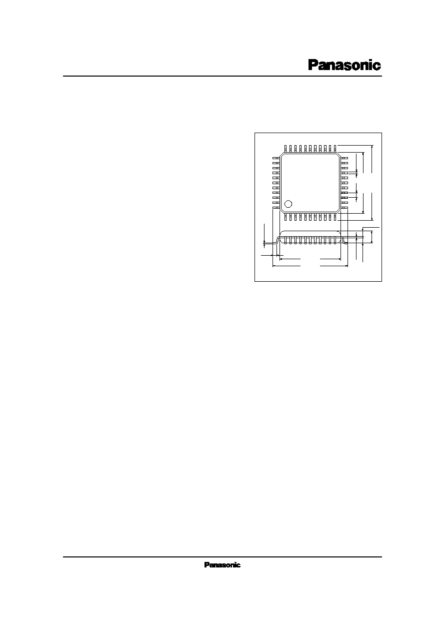
AN8819NFB
4Ch. Linear Driver IC + DC-DC Converter Control for CD
Unit : mm
1
11
12
22
33
23
44
34
0.3
+ 0.1
≠ 0.05
0.8
10.0
±
0.3
12.2
±
0.4
12.2
±
0.4
10.0
±
0.3
(0.6)
0.1
±
0.1
2.0
±
0.3
0.9
±
0.1
0.9
±
0.1
0.2
+ 0.1
≠ 0.05
44-lead QFP package (QFP044-P-1010)
AN8819NFB
ICs for CD/CD-ROM Player
s
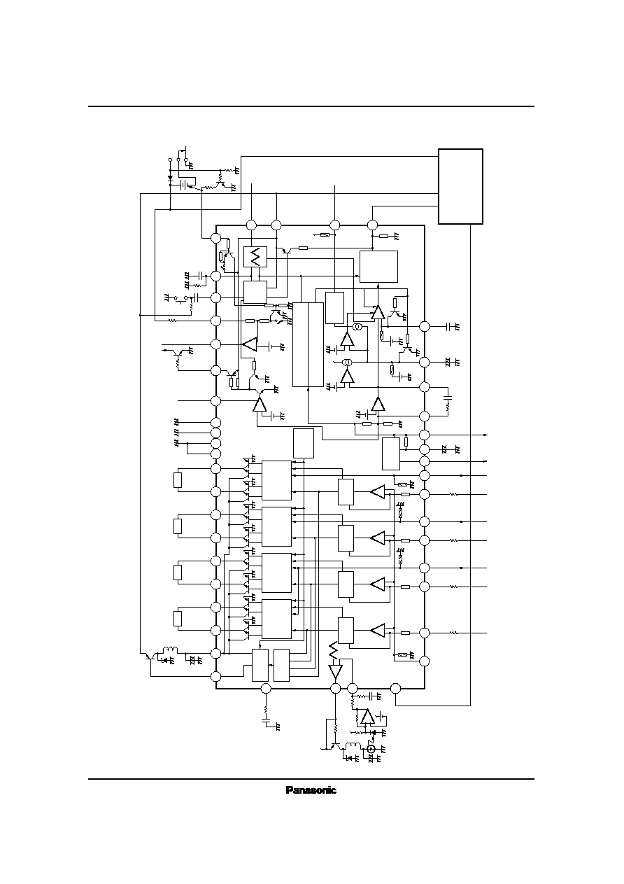
Block Diagram
B
T
L
B
T
L
B
T
L
B
T
L
+
≠
+
≠
+
≠
2
6
2
5
2
4
2
3
2
9
3
0
3
1
3
2
2
8
2
7
6
3
5
7
4
3
4
4
1
5
1
6
1
7
1
8
1
9
2
0
2
1
2
2
3
4
3
3
4
2
+
≠
+
≠
+
≠
3
6
3
7
3
9
4
1
9
3
8
1
4
0
3
1
3
1
2
1
1
5
4
8
2
P
O
W
E
R
O
F
F
+
≠
+
≠
+
≠
1
4
1
0
P
W
M
+
≠
+
≠
+
≠
+
≠
+
≠
M
a
x
.
V
a
l
u
e
A
b
s
o
l
u
t
e
V
a
l
u
e
R
i
p
p
l
e
F
i
l
t
e
r
D
C
-
D
C
C
o
n
v
.
S
w
i
t
c
h
i
n
g
C
i
r
c
u
i
t
S
t
a
r
t
e
r
e
x
c
h
a
n
g
e
I
n
i
t
i
a
l
s
e
t
t
i
n
g
T
h
e
r
m
a
l
S
h
u
t
d
o
w
n
S
t
a
r
t
e
r
A
b
s
o
l
u
t
e
V
a
l
u
e
A
b
s
o
l
u
t
e
V
a
l
u
e
A
b
s
o
l
u
t
e
V
a
l
u
e
D
R
V
C
C
S
V
C
C
P
G
N
D
S
G
N
D
P
V
C
C
ICs for CD/CD-ROM Player
AN8819NFB
s
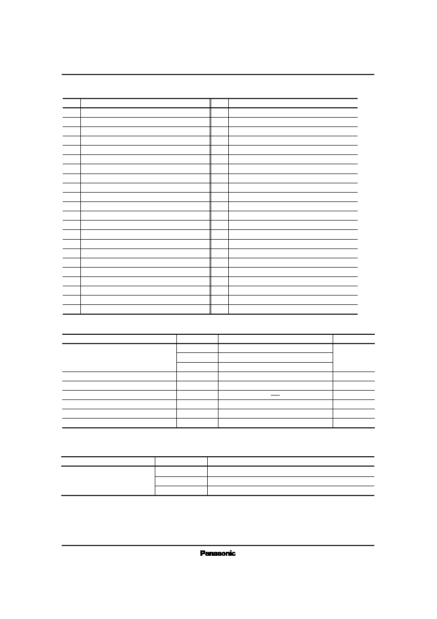
Pin Description
Pin No.
Pin Name
1
2
3
4
5
6
7
8
9
10
11
12
13
14
15
16
17
18
19
20
21
22
PV
CC
Supply Pin
DED Dead Time Input Pin
OUT DC-DC Converter Output Pin
FB Error Amp. Input Pin
IN Error Amp. Output Pin
DRGND Ground Pin
SGND Ground Pin
SPRO Short-Circuit Protection Input Pin
BSEL Empty Detection Level Changeover Pin
V
SEN
Empty Detection Input Pin
SV
CC
Power Pin
CRIP Capacitor Pin for Ripple Rejection
AVDD Ripple Filter Ouput Pin
DRV
CC
Supply Pin
V
REF
1/2 V
CC
Input Pin
INFO Driver Input Pin
INTR Driver Input Pin
LDON Driver ON ≠ OFF Control Pin
INSP Driver Input Pin
PC Driver ON ≠ OFF Control Pin
INTV Driver Input Pin
TRVSTOP Driver ON ≠ OFF Control Pin
Pin No.
Pin Name
23
24
25
26
27
28
29
30
31
32
33
34
35
36
37
38
39
40
41
42
43
44
TR≠ Driver Output Pin
TR+ Driver Output Pin
FO ≠ Driver Output Pin
FO + Driver Output Pin
PGND Ground Pin
PGND Ground Pin
SP + Driver Output Pin
SP ≠ Driver Output Pin
TV+ Driver Output Pin
TV≠ Driver Output Pin
VC Driver Power Voltage Pin
TB PWM Circuit Output Pin
RESET Reset Output Pin
MRST Muting Reset Output Pin
EMP Empty Detection Output Pin
CLK External Synchronization Input Pin
START Start Oscillation Start Input Pin
POWER Power On/Off Input Pin
CT Triangular Wave Oscillation Pin
PWMG PWM Loop Gain Adjustment Pin
COMPO APC Comparator Output Pin
COMPI APC Comparator Input Pin
s
Absolute Maximum Ratings
(Ta=25∞C)
PV
CC
SV
CC
DRV
CC
V
10max.
V
33max.
I
CC
P
D
T
opr
T
stg
Supply Voltage
V
SEN
Pin Maximum Applied Voltage
V
C
Pin Maximum Applied Voltage
Supply Current
Power Dissipation
Note)
Operating Ambient Temperature
Storage Temperature
V
V
V
mA
mW
∞C
∞C
Parameter
Symbol
Rating
Unit
15
6
6
15
9
880
≠25 ~ + 75
≠55 ~ + 125
Note) Unit
s
Recommended Operating Range
(Ta=25∞C)
Parameter
Symbol
Range
Operating Supply Voltage Range
PV
CC
SV
CC
DRV
CC
1.5V ~ 9V
2.7V ~ 5.5V
2.7V ~ 5.5V

AN8819NFB
ICs for CD/CD-ROM Player
Parameter
Symbol
Condition
min.
typ.
max.
Unit
s
Electrical Characteristics
(Ta=25∞C
±
2∞C)
Driver Portion
V
DMAX
I
DMAX
G
+
G
sp +
V
OFF
V
SPOFF
I
DZ
I
SpDZ
V
mA
k
k
mV
mV
µ
A
µ
A
2.0
1.8
1.8
4.5
3.0
5.1
2.0
43
87
SV
CC
No Load Supply Current
DRV
CC
No Load Supply Current
PV
CC
No Load Supply Current
PV
CC
Leak Current
I
11Q
I
14Q
I
1Q
I
1L
PV
CC
= 2.4V, SV
CC
= DRV
CC
= 3.2V, V
REF
= 1.6V
3.1
2.4
2.6
mA
mA
mA
µ
A
500
33
67
≠50
≠100
≠1
≠2
DRV
CC
≠1.2
53
107
50
100
1
2
Maximum Drive Voltage
of Pins FO, TR, SP and TV
Ripple Rejection Ratio
R
R13
40
dB
PV
CC
= 4V,
SV
CC
= DRV
CC
= 3.2V
PV
CC
= 4V,
SV
CC
= DRV
CC
= 3.2V
PV
CC
= 4V,
SV
CC
= DRV
CC
= 3.2V
PV
CC
= 4V,
SV
CC
= DRV
CC
= 3.2V
PV
CC
= 4V,
SV
CC
= DRV
CC
= 3.2V
PV
CC
= 4V,
SV
CC
= DRV
CC
= 3.2V
PV
CC
= 4V,
SV
CC
= DRV
CC
= 3.2V
DC-DC Converter Portion
%
%
%
V
V
kHz
kHz
74
80
45
1.5
0.3
83
65
PV
CC
= 2.4V, SV
CC
= DRV
CC
= 3.2V, CT
= 390pF/470k
,
V
IN
= 0.8V
65
74
35
1.08
0.15
60
54
83
86
55
1.71
0.4
115
76
PV
CC1
= 2.4V, SV
CC
= DRV
CC
= 3.2V, V
REF
= 1.6V
PV
CC1
= 2.4V, SV
CC
= DRV
CC
= 3.2V, V
REF
= 1.6V
PV
CC
= 9V, SV
CC
= DRV
CC
= 0V, V
ERF
= 0V
Maximum Drive Current
Focus/Tracking/Traverse
Transmission Gain (+)
Spindle Transmission Gain (+)
Focus/Tracking/Traverse
Output Offset Voltage
Spindle Output Offset Voltage
Focus/Tracking/Traverse
Input Conversion Dead Zone
Spindle Input Conversion Dead Zone
PV
CC
= 4V,
SV
CC
= DRV
CC
= 3.2V
D
2C
D
2F
D
2S
V
20H
V
20L
F
41S
F
41F
PV
CC
= 2.4V, SV
CC
= DRV
CC
= 3.2V, CT
= 390pF/470k
,
V
IN
= 0.8V
PV
CC
= 2.4V, SV
CC
= DRV
CC
= 3.2V, CT
= 390pF/470k
,
V
IN
= 0.8V
PV
CC
= 2.4V, SV
CC
= 3.2V
I
OUT
= ≠25mA,
V
CT
= 0V, V
FB
= 0.7V
PV
CC
= 2.4V, SV
CC
= DRV
CC
= 3.2V, I
OUT
= 15mA,
V
CT
= 1V, V
FB
= 0.5V
PV
CC
= 3.2V, SV
CC
= 0V
CT
= 390pF/470k
PV
CC
= 2.4V, SV
CC
= DRV
CC
= 3.2V, CT
= 390pF/470k
PV
CC
= 2.4V, SV
CC
= DRV
CC
= 3.2V, Input
= 35mVrms/20kHz
Ripple Filter Portion
CLK Synchronization Output Pulse
Maximum Duty
Self-Running Output Pulse
Maximum Duty
Starting Output Pulse Maximum Duty
Self-Running Output Voltage (H)
Self-Running Output Voltage (L)
Starting Oscillation Frequency
Self-Running Oscillation Frequency
ICs for CD/CD-ROM Player
AN8819NFB
s
Pin Description
Pin Description
Equivalent Circuit
Pin No.
11
7
14
6
1
Symbol
I/O
27
28
2
3
SV
CC
SGND
DRV
CC
DRGND
PV
CC
PGND
DED
OUT
I
I
I
I
I
I
O
Supply pin for control circuits
other than of driver, not connected
with DRV
CC
, PV
CC
Ground pin for control circuits
other than of driver
Supply pin for control circuit of
driver, not connected with SV
CC
,
PV
CC
Ground pin for control circuit of
driver
Supply pin supplying the current
for output power transistor
Ground pin for output power
transistor
Setting pin for dead time control
input and soft start
Switching output pin
11
7
14
1
2
6
27
28
50k
200
15k
25k
SV
CC
3
PV
CC