 | –≠–ª–µ–∫—Ç—Ä–æ–Ω–Ω—ã–π –∫–æ–º–ø–æ–Ω–µ–Ω—Ç: DN8797MS | –°–∫–∞—á–∞—Ç—å:  PDF PDF  ZIP ZIP |

Hall ICs
1
Publication date: November 2002
SPC00008CJB
DN8797MS
3 V operation Hall IC
One-way magnetic field operation
Overview
The DN8797MS is a 3 V operation Hall IC which
includes a Hall element, amplifier circuit, Schmidt circuit,
stabilized power supply and temperature compensation cir-
cuit which are integrated on a single chip with a fine pat-
terning technology. The magnetic input signal is output-
ted by being converted to high or low. We have improved
the conventional circuit to realize a stable operation cov-
ering from low to high supply voltage and from low to
high temperature.
Features
∑ Wide operating supply voltage range
(V
CC
= 2.7 V to 14.4 V)
∑ Wide operating ambient temperature (-40∞C to +85∞C)
∑ Package: Mini type (3-pin type)
(1.1 mm thick: Same as a standard transistor)
∑ Eqipped with an output pull-up resistor (typical 56 k)
Applications
∑ DC brushless motor, fan motor, rotation sensor, detec-
tion of cover open/close (example for a cellular phone),
position sensor
Block Diagram
Unit: mm
MINI-3D
2
V
CC
1
Out
3
GND
56 k
(typ.)
Constant
voltage source
Hall element
Amplifier
Comparator
2.80
+0.20
≠0.30
1.50
+0.25
≠0.05
0.65±0.15
0.65±0.15
3
1
2
0.95
0.95
1.90±0.20
0.40
+0.10 ≠0.05
1.10
+0.20 ≠0.10
0.80
0.40±0.20
0.16
+0.10 ≠0.06
1.45
0.10 to 0.30
2.90
+0.20 ≠0.05
0 to 0.10
Note) The package of this product will be changed
to lead-free type (MINI-3DA). See the new
package dimensions section later of this
datasheet.

2
DN8797MS
SPC00008CJB
Note) 1. Symbol B
H-L
stands for the operating magnetic flux density where its output level varies from high to low.
2. Symbol B
L-H
stands for the operating magnetic flux density where its output level varies from low to high.
3. The variation of operating magnetic flux density does not depend on supply voltage due to its built-in stabilized power
source. (V
CC
should be confined to the range of 2.7 V to 14.4 V.)
4. A supply current changes by maximum 1 mA when its output level varies from high to low.
Pin Descriptions
Pin No.
Symbol
Description
1
Out
Output pin
2
V
CC
Supply voltage pin
3
GND
Ground pin
Recommended Operating Range
Parameter
Symbol
Range
Unit
Supply voltage
V
CC
2.7 to 14.4
V
Absolute Maximum Ratings
Parameter
Symbol
Rating
Unit
Supply voltage
V
CC
18
V
V
OUT
18
Supply current
I
CC
mA
Power dissipation
P
D
120
mW
Operating ambient temperature
T
opr
-20 to +85
∞C
Storage temperature
T
stg
-55 to +125
∞C
Note) 1. Except for the operating ambient temperature and storage temperature, all ratings are for T
a
= 25∞C.
2. The reverse insertion of this IC will cause its breakdown.
3. It will operate normally in several tens of ms after power on.
4. This IC is not suitable for car electrical equipment.
Electrical Characteristics at T
a
= 25∞C
Parameter
Symbol
Conditions
Min
Typ
Max
Unit
Operating magnetic flux density 1
B
H-L
V
CC
= 3 V
-20
mT
Operating magnetic flux density 2
B
L-H
V
CC
= 3 V
-3
mT
Hysteresis width
BW
V
CC
= 3 V
0.2
1.5
4
mT
Output voltage 1
V
OL1
V
CC
= 14.4 V, I
O
= 5 mA, B = -22 mT
0.07
0.30
V
Output voltage 2
V
OL2
V
CC
= 2.7 V, I
O
= 5 mA, B = -22 mT
0.07
0.30
V
Output voltage 3
V
OH1
V
CC
= 14.4 V, I
O
= -20 µA, B = -3 mT 12.8
13.3
13.8
V
Output voltage 4
V
OH2
V
CC
= 2.7 V, I
O
= -20 µA, B = -3 mT
1.05
1.55
2.05
V
Output short-circuited current
-I
OS
V
CC
= 14.4 V, B = -3 mT, V
O
= 0 V
0.19
0.27
0.39
mA
Supply current 1
I
CC1
V
CC
= 14.4 V, B = -3 mT
1.0
3.4
6.0
mA
Supply current 2
I
CC2
V
CC
= 2.7 V, B = -3 mT
1.0
2.5
6.0
mA

3
DN8797MS
SPC00008CJB
Technical Data
∑ Position of a Hall element (unit in mm)
Distance from a package surface to sensor part: 0.71 mm
A Hall element is placed on the shaded part in the figure.
0.5
0.5
1.2
0.5
∑ Magneto-electro conversion characteristics
Direction of applied magnetic field
Applied magnetic flux density B
Output v
oltage
S
N
BW
B
H-L
B
L-H

4
DN8797MS
SPC00008CJB
V
CC
=
3.0 V, Pull-Up-R.
= 56 k
Output Rise Time
Sample. 1
Sample. 2
Sample. 3
Sample. 4
Sample. 5
Average
- aooliedmagnetic field (µs)
8.98
7.72
9.18
8.06
8.78
8.74
+ aooliedmagnetic field (ns)
292
318
356
280
320
313
3
(V)
2
1
0
0
10
t (ns)
V
CC
= 3 V
3
(V)
2
1
0
0
10
Output Rise Time
t (ns)
- applied magnetic field
90%
10%
3
(V)
2
1
0
0
1
Output Rise Time
t (
µs)
- applied magnetic field
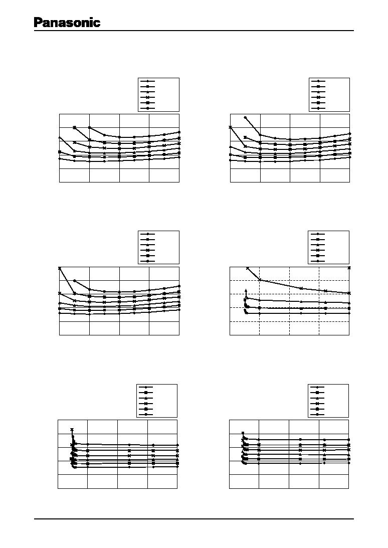
Technical Data (continued)
∑ Output Rise Time
5
DN8797MS
SPC00008CJB
I
O
= 10 mA
I
O
= 9 mA
I
O
= 8 mA
I
O
= 7 mA
I
O
= 6 mA
I
O
= 5 mA
Output Low voltage (V)
0.25
0.20
0.15
0.10
0.05
0
-50
0
50
100
150
Ambient temperature (
∞C)
I
O
= 10 mA
I
O
= 9 mA
I
O
= 8 mA
I
O
= 7mA
I
O
= 6 mA
I
O
= 5 mA
Output Low voltage (V)
0.25
0.20
0.15
0.10
0.05
0
-50
0
50
100
150
Ambient temperature (
∞C)
I
O
= 10 mA
I
O
= 9 mA
I
O
= 8 mA
I
O
= 7 mA
I
O
= 6 mA
I
O
= 5 mA
Output Low voltage (V)
0.25
0.20
0.15
0.10
0.05
0
-50
0
50
100
150
Ambient temperature (
∞C)
I
O
= 10 mA
I
O
= 9 mA
I
O
= 8 mA
I
O
= 7 mA
I
O
= 6 mA
I
O
= 5 mA
Output Low voltage (V)
0.25
0.20
0.15
0.10
0.05
0
0
5
10
15
20
Supply voltage (V)
I
O
= 10 mA
I
O
= 9 mA
I
O
= 8 mA
I
O
= 7 mA
I
O
= 6 mA
I
O
= 5 mA
Output Low voltage (V)
0.25
0.20
0.15
0.10
0.05
0
0
5
10
15
20
Supply voltage (V)
I
O
= 10 mA
I
O
= 9 mA
I
O
= 8 mA
I
O
= 7 mA
I
O
= 6 mA
I
O
= 5 mA
Output Low voltage (V)
0.25
0.20
0.15
0.10
0.05
0
0
5
10
15
20
Supply voltage (V)
Technical Data (continued)
∑ Main characterisitcs
Output low voltage
Ambient temperature (V
CC
= 2.7 V)
Output low voltage
Ambient temperature (V
CC
= 5.0 V)
Output low voltage
Ambient temperature (V
CC
= 20 V)
Output low voltage
Supply voltage (Temp. = -50∞C)
Output low voltage
Supply voltage (Temp. = 25∞C)
Output low voltage
Supply voltage (Temp. = 150∞C)

6
DN8797MS
SPC00008CJB
I
O
= 20 V
I
O
= 2.7 V
Pull-up resistor (k
)
90
80
70
60
50
40
85
75
65
55
45
-50
0
50
100
150
Ambient temperature (
∞C)
Pull-up resistor (k
)
90
80
70
60
50
40
85
75
65
55
45
Temp.
= 150∞C
Temp.
= 25∞C
Temp.
= -50∞C
0
5
10
15
20
Supply voltage (V)
V
CC
= 20 V(Output = Low)
V
CC
= 20 V(Output = High)
V
CC
= 5.0 V(Output = Low)
V
CC
= 5.0 V(Output = High)
V
CC
= 2.7 V(Output = Low)
V
CC
= 2.7 V(Output = High)
Supply current (mA)
7
5
3
1
6
4
2
0
-50
0
50
100
150
Ambient temperature (
∞C)
Temp.
= 150∞C (Output = Low)
Temp.
= 150∞C (Output = High)
Temp.
= 25∞C (Output = Low)
Temp.
= 25∞C (Output = High)
Temp.
= -50∞C(Output = Low)
Temp.
= -50∞C (Output = High)
Supply current (mA)
7
5
3
1
6
4
2
0
0
5
10
15
20
Supply voltage (V)
Technical Data (continued)
∑ Main characterisitcs (continued)
Pull-up resistor
Ambient temperature
Pull-up resistor
Supply voltage
Supply current
Ambient temperature
Supply current
Supply voltage
7
DN8797MS
SPC00008CJB
B
H-L
-3
B
L-H
-3
B
H-L
-2
B
L-H
-2
B
H-L
-1
B
L-H
-1
-15
-10
-5
-20
-50
0
50
100
150
Ambient temperature (
∞C)
0
5
10
15
Operating magnetic flux density (mT)
B
H-L
-3
B
L-H
-3
B
H-L
-2
B
L-H
-2
B
H-L
-1
B
L-H
-1
-15
-10
-5
-20
-50
0
50
100
150
Ambient temperature (
∞C)
0
5
10
15
Operating magnetic flux density (mT)
-15
-10
-5
-20
-50
0
50
100
150
Ambient temperature (
∞C)
0
5
10
15
Operating magnetic flux density (mT)
B
H-L
-3
B
L-H
-3
B
H-L
-2
B
L-H
-2
B
H-L
-1
B
L-H
-1
B
H-L
(Temp.
= 150∞C)
B
L-H
(Temp.
= 150∞C)
B
H-L
(Temp.
= -50∞C)
B
L-H
(Temp.
= -50∞C)
-20
0
5
10
15
20
-15
-10
-5
0
5
10
Operating magnetic flux density (mT)
Supply voltage (V)
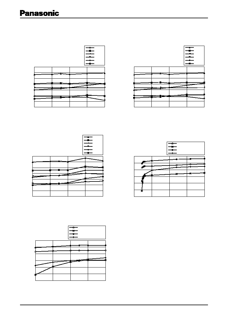
Technical Data (continued)
∑ Main characterisitcs (DN8796MS/DN8798MS) (continued)
Operating magnetic flux density
Ambient temperature (V
CC
= 2.7 V) Operating magnetic flux density Ambient temperature (V
CC
= 3.0 V)
Operating magnetic flux density
Ambient temperature (V
CC
= 20 V)
Operating magnetic flux density
Supply voltage
-20.0
2.2
2.4
2.6
2.8
3.0
-15.0
-10.0
-5.0
0.0
5.0
10.0
B
H-L
(Temp.
= 150∞C)
B
L-H
(Temp.
= 150∞C)
B
H-L
(Temp.
= -50∞C)
B
L-H
(Temp.
= -50∞C)
Operating magnetic flux density (mT)
Supply voltage (V)
Operating magnetic flux density
Supply voltage

8
DN8797MS
SPC00008CJB
B
H-L
-3
B
L-H
-3
B
H-L
-2
B
L-H
-2
B
H-L
-1
B
L-H
-1
-50
0
50
100
150
25
0
5
10
15
20
Ambient temperature (
∞C)
Operating magnetic flux density (mT)
B
H-L
-3
B
L-H
-3
B
H-L
-2
B
L-H
-2
B
H-L
-1
B
L-H
-1
-50
0
50
100
150
25
0
5
10
15
20
Ambient temperature (
∞C)
Operating magnetic flux density (mT)
B
H-L
-3
B
L-H
-3
B
H-L
-2
B
L-H
-2
B
H-L
-1
B
L-H
-1
-50
0
50
100
150
25
0
5
10
15
20
Ambient temperature (
∞C)
Operating magnetic flux density (mT)
B
H-L
(Temp. = 125
∞C)
B
L-H
(Temp. = 125
∞C)
B
H-L
(Temp. =
-50∞C)
B
L-H
(Temp. =
-50∞C)
Operating magnetic flux density (mT)
20
18
16
14
12
10
0
5
10
15
20
Supply voltage (V)
Technical Data (continued)
∑ Main characterisitcs (DN8797MS/DN8799MS) (continued)
Operating magnetic flux density
Ambient temperature (V
CC
= 2.7 V) Operating magnetic flux density Ambient temperature (V
CC
= 3.0 V)
Operating magnetic flux density
Ambient temperature (V
CC
= 20 V)
Operating magnetic flux density
Supply voltage
B
H-L
(Temp. = 125
∞C)
B
L-H
(Temp. = 125
∞C)
B
H-L
(Temp. =
-50∞C)
B
L-H
(Temp. =
-50∞C)
Operating magnetic flux density (mT)
20
18
16
14
12
10
2.2
2.4
2.6
2.8
3.0
Supply voltage (V)
Operating magnetic flux density
Supply voltage
Operating magnetic flux density
Supply voltage
BW (Temp.
= 125∞C)
BW (Temp.
= -50∞C)
Operating magnetic flux density (mT)
5
4
3
2
1
0
0
5
10
15
20
Supply voltage (V)

9
DN8797MS
SPC00008CJB
Caution on Use of Hall ICs
The Hall ICs are often used to detect movement. In such cases, the position of the Hall IC may be changed by
exposition to shock or vibration over a long period of time, and it causes the detection level change. To prevent this, fix
the package with adhesives or fix it on a dedicated case.
1. A case using an adhesive
Some kinds of adhesive generate corrosive gas (such as chloric gas) during curing. This corrosive gas corrodes the
aluminum on the surface of the Hall IC, and may cause a functional defect of disconnection.
If Hall IC is to be sealed after installation, attention should be given to the adhesive or resin used for peripherals
and substrate cleaner, as well as to the adhesive used for Hall IC installation. Please confirm the above matter to those
manufacturers before using.
We could not select the specified adhesive, for we find it difficult to guarantee the ingredient of each adhesive.
2. Power supply line/Power transmission line
If a power supply line/power transmission line becomes longer, noise and/or oscillation may be found on the line.
In this case, set the capacitor of 0.1
µF to 10 µF near the Hall IC to prevent it.
If a voltage of 18 V or more is thought to be applied to the power supply line (flyback voltage from coil or the
ignition pulse, etc.), avoid it with external components (capacitor, resistor, Zener diode, diode, surge absorbing elements,
etc.).
3. On mounting of the surface mount type package (MINI-3D)
When mounted on the printed circuit board, the Hall IC may be highly stressed by the warp that may occur from
the soldering. This may also cause a change in the operating magnetic flux density and a deterioration of its resistance
to moisture.
4. V
CC
and GND
Do not reverse V
CC
and GND. If the V
CC
and GND pins are reversely connected, this IC will be destroyed. If the
IC GND-pin voltage is set higher than other pin voltage, the IC configuration will become the same as a forward
biased diode. Therefore, it will turn on at the diode forward voltage (approximately 0.7 V), and a large current will
flow through the IC, ending up in its destruction. (This is common to monolithic IC.)
5. Cautions on power-on of Hall IC
When a Hall IC is turned on, the position of the magnet or looseness may change the output of a Hall IC, and a pulse
may be generated. Therefore, care should be given whenever the output state of a Hall IC is critical when the supply
power is on.
6. On fixing a Hall IC to holder
When a Hall IC is mounted on the printed circuit board with a holder and the coefficient of expansion of the holder
is large, the lead wire of the Hall IC will be stretched and it may give a stress to the Hall IC.
If the lead wire is stressed intensely due to the distortion of holder or board, the adhesives between the package
and the lead wire may be weakened and cause a minute gap resulting in the deterioration of its resistance to moisture.
Sensitivity may also be changed by this stress.
7. On using flux in soldering
Choose a flux which does not include ingredients from halogen group, such as chlorine, fluorine, etc. The
ingredients of halogen group may enter where the lead frame and package resin joint, causing corrosion and the
disconnection of the aluminum wiring on the surface of an IC chip.
8. In case of the magnetic field of a magnet is too strong
Output may be inverted when applying a magnetic flux density of 100 mT or more. Accordingly, magnetic flux
density should be used within the range of 100 mT.
9. On surface treatment of mini-mold package
Surface treatment is available in either smooth or dull finish.
10. On soldering of the surface mount type package
Surface mounting type Hall ICs are apt to change its electrical characteristics due to the stress from soldering at
mounting. Therefore, avoid the mounting by flow (dipping) and a soldering iron. Please mount it by reflow soldering
abiding by its recommended conditions.
Correct
Wrong

10
DN8797MS
SPC00008CJB
New Package Dimensions (Unit: mm)
∑ MINI-3DA (Lead-free package)
2
3
1
0.11
+0.10 -
0.05
Seating plane
0 to 0.10 0.40
±0.20
1.10
+0.30 -
0.10
0.10 to 0.30
1.10
+0.20 -
0.10
1.50
+0.25 -
0.05
0.40
+0.10
-0.05
(1.45)
0.65
±
0.15
2.80
+0.20 -
0.30
1.90
±0.20
0.65
±
0.15
2.90
+0.20
-0.05
0.95
0.95
0.10
M
0.10

Request for your special attention and precautions in using the technical information
and semiconductors described in this material
(1) An export permit needs to be obtained from the competent authorities of the Japanese Government
if any of the products or technologies described in this material and controlled under the "Foreign
Exchange and Foreign Trade Law" is to be exported or taken out of Japan.
(2) The technical information described in this material is limited to showing representative characteris-
tics and applied circuits examples of the products. It neither warrants non-infringement of intellec-
tual property right or any other rights owned by our company or a third party, nor grants any license.
(3) We are not liable for the infringement of rights owned by a third party arising out of the use of the
product or technologies as described in this material.
(4) The products described in this material are intended to be used for standard applications or general
electronic equipment (such as office equipment, communications equipment, measuring instru-
ments and household appliances).
Consult our sales staff in advance for information on the following applications:
∑ Special applications (such as for airplanes, aerospace, automobiles, traffic control equipment,
combustion equipment, life support systems and safety devices) in which exceptional quality and
reliability are required, or if the failure or malfunction of the products may directly jeopardize life or
harm the human body.
∑ Any applications other than the standard applications intended.
(5) The products and product specifications described in this material are subject to change without
notice for modification and/or improvement. At the final stage of your design, purchasing, or use of
the products, therefore, ask for the most up-to-date Product Standards in advance to make sure that
the latest specifications satisfy your requirements.
(6) When designing your equipment, comply with the guaranteed values, in particular those of maxi-
mum rating, the range of operating power supply voltage, and heat radiation characteristics. Other-
wise, we will not be liable for any defect which may arise later in your equipment.
Even when the products are used within the guaranteed values, take into the consideration of
incidence of break down and failure mode, possible to occur to semiconductor products. Measures
on the systems such as redundant design, arresting the spread of fire or preventing glitch are
recommended in order to prevent physical injury, fire, social damages, for example, by using the
products.
(7) When using products for which damp-proof packing is required, observe the conditions (including
shelf life and amount of time let standing of unsealed items) agreed upon when specification sheets
are individually exchanged.
(8) This material may be not reprinted or reproduced whether wholly or partially, without the prior written
permission of Matsushita Electric Industrial Co., Ltd.
2002 JUL