1
PNA1801L (PN168)
Silicon NPN Phototransistor
For optical control systems
Features
High sensitivity
Wide spectral sensitivity, suited for detecting GaAs LEDs
Small size, high output power, low cost
Ý 3 plastic package
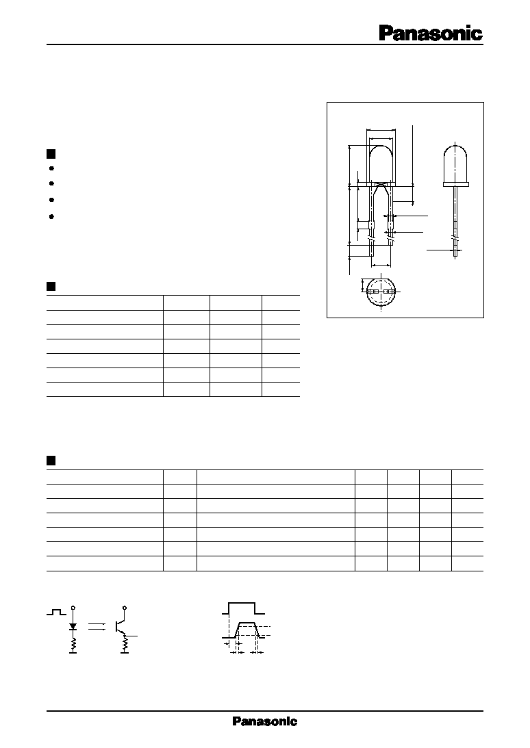
Phototransistors
1: Emitter
2: Collector
Ý3.0
Ī
0.2
Ý3.8
Ī
0.2
2-0.8 max.
2-0.5
Ī
0.1
0.5
Ī
0.1
2.54
5.0
Ī
0.2
1.7
15.0
Ī
1.0
4.5
Ī
0.3
0.6
1.0
(1.5)
1
2
Not soldered 2.0 max.
Unit : mm
;;
;;
;
;
(Input pulse)
(Output pulse)
50
R
L
t
d
: Delay time
t
r
: Rise time (Time required for the collector photo current to
increase from 10% to 90% of its final value)
t
f
: Fall time (Time required for the collector photo current to
decrease from 90% to 10% of its initial value)
V
CC
Sig.OUT
10%
90%
Sig.IN
t
d
t
r
t
f
Absolute Maximum Ratings
(Ta = 25įC)
Parameter
Symbol
Ratings
Unit
Collector to emitter voltage
V
CEO
30
V
Emitter to collector voltage
V
ECO
5
V
Collector current
I
C
20
mA
Collector power dissipation
P
C
100
mW
Operating ambient temperature
T
opr
≠25 to +85
įC
Storage temperature
T
stg
≠30 to +100
įC
Electro-Optical Characteristics
(Ta = 25įC)
Parameter
Symbol
Conditions
min
typ
max
Unit
Dark current
I
CEO
V
CE
= 10V
0.005
0.5
Ķ
A
Collector photo current
I
CE(L)
V
CE
= 10V, L = 500 lx
*1
0.8
3
mA
Peak sensitivity wavelength
P
V
CE
= 10V
800
nm
Acceptance half angle
Measured from the optical axis to the half power point
35
deg.
Response time
t
r
, t
f
*2
V
CC
= 10V, I
CE(L)
= 1mA, R
L
= 100
4
Ķ
s
Collector saturation voltage
V
CE(sat)
I
CE(L)
= 1mA, L = 1000 lx
*1
0.2
0.5
V
*1
Measurements were made using a tungsten lamp (color temperature T = 2856K) as a light source.
*2
Switching time measurement circuit
Note) The part number in the parenthesis shows conventional part number.

2
Phototransistors
PNA1801L
t
r
-- I
CE(L)
Collector photo current I
CE(L)
(mA)
Rise time t
r
(
Ķ
s)
Ta = 25įC
10
4
10
3
10
2
10
1
10
≠1
10
≠1
10
10
2
1
10
≠2
t
f
-- I
CE(L)
Collector photo current I
CE(L)
(mA)
Fall time t
f
(
Ķ
s)
Ta = 25įC
10
4
10
3
10
2
10
1
10
≠1
10
≠1
10
10
2
1
10
≠2
P
C
-- Ta
120
100
80
60
40
20
Ambient temperature Ta (įC )
Collector power dissipation P
C
(mW)
0
20
40
60
80
100
0
≠ 20
Ta = 25įC
T = 2856K
I
CE(L)
-- V
CE
20
16
12
4
8
0
Collector to emitter voltage V
CE
(V)
Collector photo current I
CE(L)
(mA)
0
20
16
8
12
4
24
Spectral sensitivity characteristics
100
80
60
40
20
Wavelength
(nm)
Relative sensitivity S (%)
400
600
800
1000
1200
0
200
V
CE
= 10V
Ta = 25įC
I
CE(L)
-- L
Illuminance L (lx)
Collector photo current I
CE(L)
(mA)
V
CE
= 10V
Ta = 25įC
T = 2856K
10
3
10
2
10
1
10
≠1
10
10
3
10
4
10
2
10
≠2
1
I
CEO
-- Ta
10
3
10
1
10
2
Ambient temperature Ta (įC )
V
CE
= 10V
Dark current I
CEO
(nA)
10
≠1
≠ 40
0
40
80
120
V
CE
= 10V
T = 2856K
I
CE(L)
-- Ta
10
2
1
10
Ambient temperature Ta (įC )
≠ 40
0
40
80
120
10
≠1
Collector photo current I
CE(L)
(mA)
0į
10į
20į
30į
40į
50į
60į
70į
80į
90į
Directivity characteristics
20
90
100
80
70
60
50
40
30
Relative sensitivity S (%)
750 lx
500 lx
L = 2000 lx
1000 lx
1500 lx
1750 lx
1250 lx
100 lx
250 lx
L = 1000 lx
500 lx
R
L
= 1k
500
100
R
L
= 1k
500
100

Please read the following notes before using the datasheets
A. These materials are intended as a reference to assist customers with the selection of Panasonic
semiconductor products best suited to their applications.
Due to modification or other reasons, any information contained in this material, such as available
product types, technical data, and so on, is subject to change without notice.
Customers are advised to contact our semiconductor sales office and obtain the latest information
before starting precise technical research and/or purchasing activities.
B. Panasonic is endeavoring to continually improve the quality and reliability of these materials but
there is always the possibility that further rectifications will be required in the future. Therefore,
Panasonic will not assume any liability for any damages arising from any errors etc. that may ap-
pear in this material.
C. These materials are solely intended for a customer's individual use.
Therefore, without the prior written approval of Panasonic, any other use such as reproducing,
selling, or distributing this material to a third party, via the Internet or in any other way, is prohibited.
Request for your special attention and precautions in using the technical information
and semiconductors described in this material
(1) An export permit needs to be obtained from the competent authorities of the Japanese Govern-
ment if any of the products or technologies described in this material and controlled under the
"Foreign Exchange and Foreign Trade Law" is to be exported or taken out of Japan.
(2) The technical information described in this material is limited to showing representative character-
istics and applied circuit examples of the products. It does not constitute the warranting of industrial
property, the granting of relative rights, or the granting of any license.
(3) The products described in this material are intended to be used for standard applications or gen-
eral electronic equipment (such as office equipment, communications equipment, measuring in-
struments and household appliances).
Consult our sales staff in advance for information on the following applications:
∑ Special applications (such as for airplanes, aerospace, automobiles, traffic control equipment,
combustion equipment, life support systems and safety devices) in which exceptional quality and
reliability are required, or if the failure or malfunction of the products may directly jeopardize life or
harm the human body.
∑ Any applications other than the standard applications intended.
(4) The products and product specifications described in this material are subject to change without
notice for reasons of modification and/or improvement. At the final stage of your design, purchas-
ing, or use of the products, therefore, ask for the most up-to-date Product Standards in advance to
make sure that the latest specifications satisfy your requirements.
(5) When designing your equipment, comply with the guaranteed values, in particular those of maxi-
mum rating, the range of operating power supply voltage and heat radiation characteristics. Other-
wise, we will not be liable for any defect which may arise later in your equipment.
Even when the products are used within the guaranteed values, redundant design is recommended,
so that such equipment may not violate relevant laws or regulations because of the function of our
products.
(6) When using products for which dry packing is required, observe the conditions (including shelf life
and after-unpacking standby time) agreed upon when specification sheets are individually exchanged.
(7) No part of this material may be reprinted or reproduced by any means without written permission
from our company.
2001 MAR