 | –≠–ª–µ–∫—Ç—Ä–æ–Ω–Ω—ã–π –∫–æ–º–ø–æ–Ω–µ–Ω—Ç: PI5V332 | –°–∫–∞—á–∞—Ç—å:  PDF PDF  ZIP ZIP |

1
PS8118A 08/23/04
Block Diagram
Features:
∑ High-performance, low-cost solution to switch between
video sources
∑ Wide bandwidth: 250 MHz
∑ Low On-Resistance: 3
∑ Low crosstalk at 10 MHz: ≠58 dB
∑ Ultra-low quiescent power (0.1µA typical)
∑ Single supply operation: +5.0V
∑ Fast switching: 10ns
∑ High-current output: 100mA
∑ Functionally equivalent to QS4A101
∑ Packaging (Pb-free & Green available):
≠ 16-pin 150-mil wide plastic QSOP (Q)
≠ 16-pin 150-mil wide plastic SOIC (W)
PI5V332
Low On-Resistance Wideband/Video
Quad with Individual Control
Description:
Pericom Semiconductor's PI5V332 is a true bidirectional Quad
Video Switch that is recommended for RGB, S-Video, or com-
posite video switching applications. The individual controls allow
for video, Hsync, or Vsync enable or disable. The switch can be
driven from a current output RAMDAC or voltage output composite
video source.
Low On-Resistance and wide bandwidth make it ideal for video and
other applications. Also this device has exceptionally high current
capability which is far greater than most analog switches offered
today. A single 5V supply is all that is required for operation.
The PI5V332 offers a high-performance, low-cost solution to switch
between video sources.
Truth Table
IN
1
IN
2
IN
3
IN
4
Function
0
X
X
X
S
A
- D
A
X
0
X
X
S
B
- D
B
X
X
0
X
S
C
- D
C
X
X
X
0
S
D
- D
D
1
1
1
1
Disconnect
Pin Description
Pin Name
Description
S
X
Analog Video I/O (Usually Inputs)
IN
X
Select Inputs
DA
X
Analog Video I/O (Usually Outputs)
GND
Ground
V
CC
Power Supply
Pin Configuration
1
2
3
4
5
6
7
8
16
15
14
13
12
11
10
9
NIC
IN
1
S
A
D
A
IN
2
S
B
D
B
GND
V
CC
IN
4
S
D
D
D
IN
3
S
C
D
C
NIC
IN
4
S
D
IN
3
S
C
IN
2
S
B
IN1
S
A
D
A
D
B
D
C
D
D

2
PS8118B 09/22/04
PI5V332
Low On-Resistance Wideband/Video
Quad with Individual Control
DC Electrical Characteristics
(Over the Operating Range, T
A
= ≠40∞C to +85∞C, V
CC
= 5V ±5%)
Parameters
Description
Test Conditions
(1)
Min.
Typ
(2)
Max.
Units
V
ANALOG
Analog Signal Range
0
--
2.0
V
V
IH
Input HIGH Voltage
Guaranteed Logic HIGH Level
2.0
--
--
V
IL
Input LOW Voltage
Guaranteed Logic LOW Level
≠0.5
--
0.8
I
IH
Input HIGH Current
V
CC
= Max., V
IN
= V
CC
--
--
±1
µA
I
IL
Input LOW Current
V
CC
= Max., V
IN
= GND
--
--
±1
I
O
Analog Output Leakage Current
0 S
1
, S
2
or D V
CC
, Switch Off
--
--
±1
V
IK
Clamp Diode Voltage
V
CC
= Min., I
IN
= ≠18 mA
--
≠0.7
≠1.2
V
I
OS
Short Circuit Current
(3)
S
1
, S
2
, D = 0V V
CC
100
--
--
mA
V
H
Input Hysteresis at Control Pins
--
150
--
mV
R
ON
Switch On-Resistance
(4)
V
CC
= Min., V
OUT
= 0.975V
R
L
= 75, I
ON
= 13mA
--
3
7
V
CC
= M
IN
., V
OUT
= 1.95V
R
L
= 75, I
ON
= 26mA
--
7
10
Maximum Ratings
(Above which the useful life may be impaired. For user guidelines, not tested.)
Storage Temperature ............................................................. ≠65∞C to +150∞C
Ambient Temperature with Power Applied ............................ ≠40∞C to +85∞C
Supply Voltage to Ground Potential (Inputs & V
CC
Only)...... ≠0.5V to +7.0V
Supply Voltage to Ground Potential (Outputs & D/O Only) ... ≠0.5V to +7.0V
DC Input Voltage ..................................................................... ≠0.5V to +7.0V
DC Output Current................................................................................ 120mA
Power Dissipation .................................................................................... 0.5W
Note:
Stresses greater than those listed under MAXIMUM RAT-
INGS may cause permanent damage to the device. This is
a stress rating only and functional operation of the device
at these or any other conditions above those indicated in
the operational sections of this specification is not implied.
Exposure to absolute maximum rating conditions for ex-
tended periods may affect reliability.
Notes:
1. For Max. or Min. conditions, use appropriate value specified under Electrical Characteristics for the applicable device type.
2. Typical values are at V
CC
= 5.0V, T
A
= 25∞C ambient and maximum loading.
3. Not more than one output should be shorted at one time. Duration of the test should not exceed one second.
4. Measured by the voltage drop between S
1
, S
2
, and D I/O pins at indicated current through the switch. On-Resistance is determined by the
lower of the voltages on the S
1
, S
2
, and D I/O pins. V
OUT
is the voltage across R
L
.
3
PS8118B 09/22/04
PI5V332
Low On-Resistance Wideband/Video
Quad with Individual Control
Dynamic Characteristics
(Over the Operating Range, T
A
= ≠40∞C to +85∞C, V
CC
= 5V ±5%)
Parameter
Description
Test Conditions
Min.
Typ.
Max.
Unit
t
ON
Turn On Time
R
L
= 75, C
L
= 20pF, see Fig. 2
--
2.5
5
ns
t
OFF
Turn Off Time
R
L
= 75, C
L
= 20pF, see Fig. 2
--
1.1
5
B
W
(1)
≠3 dB Bandwidth
R
L
= 150, see Fig. 3
250
--
--
MHz
X
TALK
Crosstalk
R
IN
= 10; R
L
= 150, 10 MHz, see Fig. 3
--
≠58
--
dB
D
G
Differential Gain
R
L
= 150, f = 3.58 MHz, see Fig. 1
--
0.64
--
%
D
P
Differential Phase
R
L
= 150, f = 3.58 MHz, see Fig. 1
--
0.27
--
Deg.
C
IN
(1)
Input/Enable Capacitance
V
IN
= 0V, f = 1 MHz
--
--
6
pF
C
OFF
(1)
Capacitance, Switch Off
V
IN
= 0V, f = 1 MHz
--
--
6
C
ON
(1)
Capacitance, Switch On
V
IN
= 0V, f = 1 MHz
--
--
20
O
IRR
Off Isolation
R
L
= 150, 10 MHz, see Fig. 3
--
≠38
--
dB
Power Supply Characteristics
Parameters
Description
Test Conditions
(1)
Min.
Typ
(2)
Max.
Units
I
CC
Quiescent Power
Supply Current
V
CC
= Max.
IN = GND or V
CC
--
0.1
3.0
µA
I
CC
Supply Current per
Input @ TTL HIGH
V
CC
= Max.
IN = 3.4V
(3)
--
--
2.5
mA
I
CCD
Supply Current per
Input per MHz
(4)
V
CC
= Max.,
S
1
, S
2
, and D Pins Open
EN = GND
Control Input Toggling
50% Duty Cycle
--
--
0.25
mA/
MHz
Notes:
1. For Max. or Min. conditions, use appropriate value specified under Electrical Characteristics for the applicable device.
2. Typical values are at V
CC
= 5.0V, +25∞C ambient.
3. Per TTL driven input (V
IN
= 3.4V, control inputs only); S
1
, S
2
, and D pins do not contribute to I
CC
.
4. This current applies to the control inputs only and represent the current required to switch internal capacitance at the specified frequency. The
S
1
, S
2
, and D I/O pins generate no significant AC or DC currents as they transition. This parameter is not tested, but is guaranteed by design.
Notes:
1. This parameter is determined by device characterization but is not production tested.
4
PS8118B 09/22/04
PI5V332
Low On-Resistance Wideband/Video
Quad with Individual Control
Definitions
Symbol
Description
R
ON
Resistance between source and drain with switch in the ON state.
I
O
Output leakage current measured at S
1
, S
2
, and D with the switch OFF.
V
IN
Digital voltage at the IN pin that selects between S
1
and S
2
analog inputs.
V
EN
A voltage that ENABLES the chip.
C
IN
Capacitance at the digital inputs.
C
OFF
Capacitance at analog I/O (S
1
, S
2
, D) with switch OFF.
C
ON
Capacitance at analog I/O (S
1
, S
2
, D) with switch ON.
V
IH
Minimum input voltage for logic HIGH.
V
IL
Minimum input voltage for logic LOW.
I
IH
(I
IL
)
Input current of the digital input.
I
OS
Minimum short circuit current for S1, S2 and D.
t
ON
Propagation delay measured between 50% of the digital input to 90% of the analog output when switch is
turned ON. The peak analog voltage is 0.714V.
t
OFF
Propagation delay measured between 50% of the digital input to 90% of the analog output when switch is
turned OFF. The peak analog voltage is 0.714V.
B
W
Frequency response of the switch in the ON state measured at 3dB down.
X
TALK
Is an unwanted signal coupled from channel to channel. Measured in ≠dB. X
TALK
= 20 LOG V
OUT
/V
IN
.
This is non-adjacent crosstalk.
D
G
Differential gain is the difference measurement between two bias levels, for instance analog input signals of
0V to 0.714V.
D
P
Differential phase is the difference measurement between two bias levels, for instance analog input signals
of 0V to 0.714V.
O
IRR
Off isolation is the resistance (measured in ≠dB) between the input and output with the switch off (NO).
5
PS8118B 09/22/04
PI5V332
Low On-Resistance Wideband/Video
Quad with Individual Control
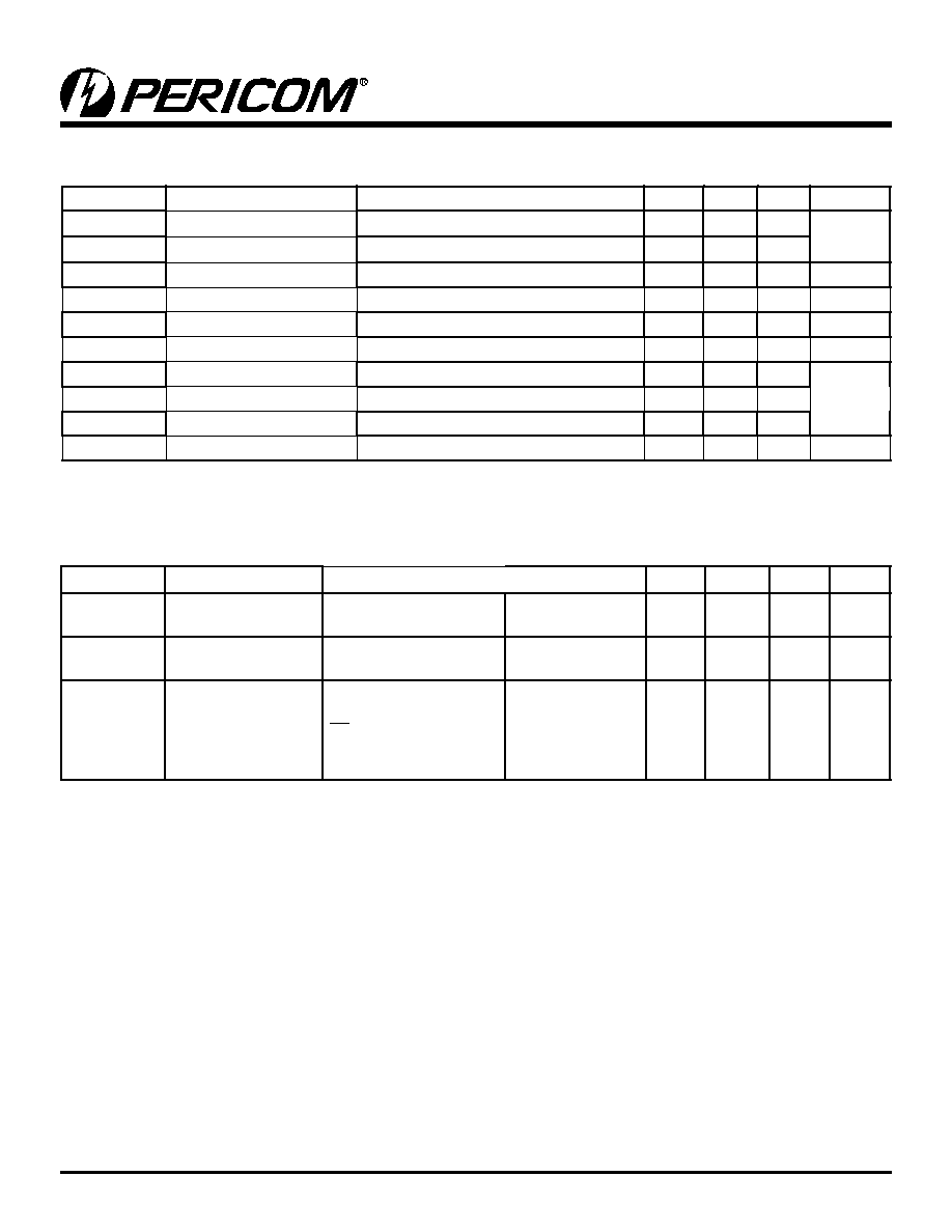
Figure 1. Differential Gain/Phase
Test Circuits
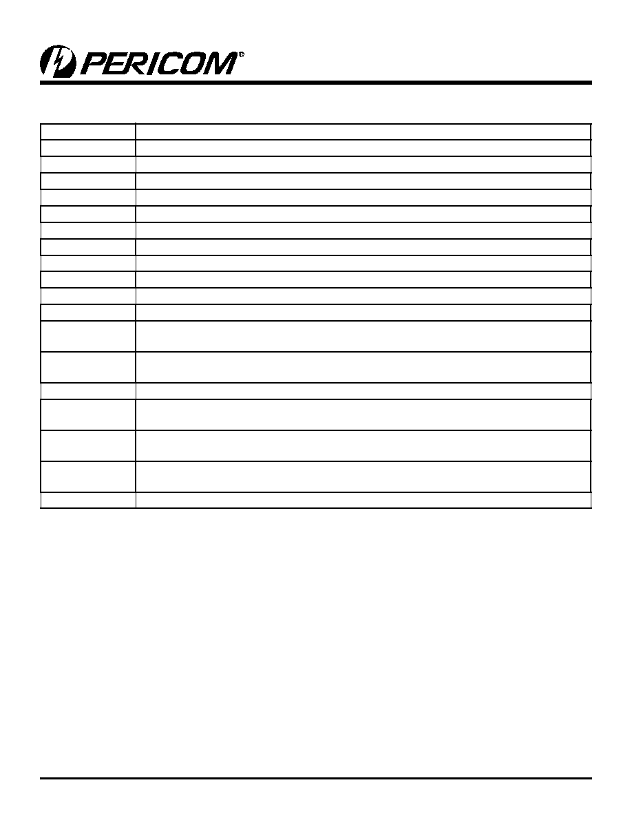
Figure 2. Switching Time
DC
S1
R1
T2
HP4195A
HP41952A
HP11667A
HP41800A
150
0.1 µF
PI5V332
0.1 mF
3V
EN
S
D
GND
PI5V332
75
+5.0V
V
CC
20pF
V
OUT
IN
Digital
Input
Analog
Output
t
ON
t
OFF
50%
90%
50%
90%
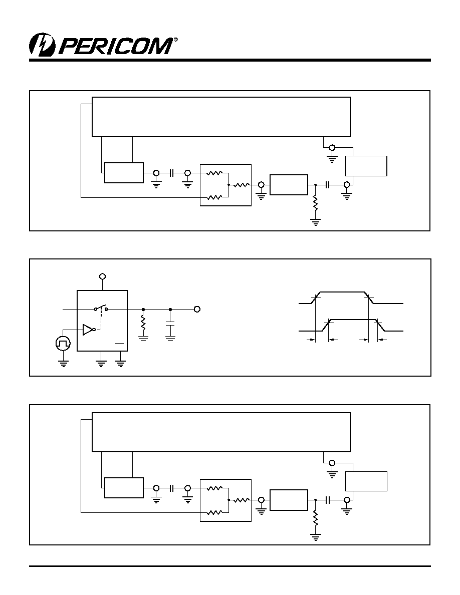
Figure 3. Gain/Phase, Crosstalk, Off-Isolation
DC
S1
R1
T2
HP4195A
HP41952A
HP11667A
HP41800A
150
0.1 µF
PI5V332
0.1 mF
6
PS8118B 09/22/04
PI5V332
Low On-Resistance Wideband/Video
Quad with Individual Control
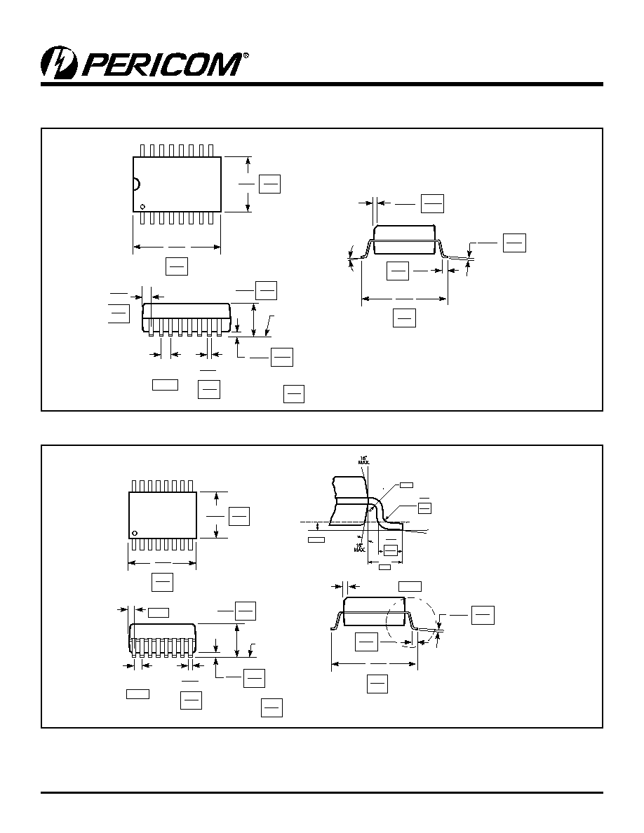
Packaging Mechanical: 16-pin SOIC (W)
Packaging Mechanical: 16-pin QSOP (Q)
SEATING PLANE
.050
BSC
1
16
0-8∞
.149
.157
X.XX
X.XX
DENOTES DIMENSIONS
IN MILLIMETERS
3.78
3.99
.386
.393
9.80
10.00
1.27
.053
.068
1.35
1.75
.2284
.2440
5.80
6.20
.0040
.0098
0.10
0.25
.013
.020
.0155
.0260
0.330
0.508
0.393
0.660
.0075
.0098
0.25
0.50
.0099
.0196
x 45∞
0.19
0.25
.016
.050
0.41
1.27
REF
.189
.197
.053
.069
.004
.010
SEATING
PLANE
.025
BSC
.007
.010
.228
.244
1
16
.150
.157
.016
.050
X.XX
X.XX
DENOTES DIMENSIONS IN MILLIMETERS
0.635
4.80
5.00
1.35
1.75
5.79
6.19
0.101
0.254
.008
.012
0.203
0.305
3.81
3.99
0.178
0.254
0.38
0.41
1.27
.008
0.203
.015 x 45
∞
REF
Detail A
Detail A
.008
0.20
MIN.
Guage Plane
.010
0.254
.041
1.04
REF
.016
.035
0.41
0.89
0∞-6∞
.008
.013
0.20
0.33
7
PS8118B 09/22/04
PI5V332
Low On-Resistance Wideband/Video
Quad with Individual Control
Pericom Semiconductor Corporation ∑ 1-800-435-2336 ∑ www.pericom.com
Ordering Information
Ordering Code
Package Code
Package Description
PI5V332W
W
16-pin SOIC
PI5V332WE
W
Pb-free & Green, 16-pin SOIC
PI5V332Q
Q
16-pin QSOP
PI5V332QE
Q
Pb-free & Green, 16-pin QSOP
Notes:
1. Thermal characteristics can be found on the company web site at www.pericom.com/packaging/