Äîêóìåíòàöèÿ è îïèñàíèÿ www.docs.chipfind.ru
1
PS8094A 03/26/97
Product Description
Pericom Semiconductor's PI74ALVCH series of logic circuits are
produced in the Company's advanced 0.5 micron CMOS technology,
achieving industry leading speed.
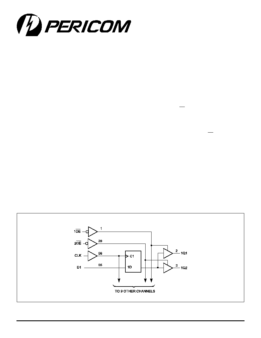
The PI74ALVCH162820 is a 10-bit flip-flop designed for 2.3V to 3.3V
V
CC
operation. The PI74ALVCH162820 is designed with edge-
triggered D-type flip-flops. On the positive transition of clock (CLK)
input, the device provides true data at the Q outputs.
A buffered output-enable (OE) input can be used to place the ten
outputs in either a normal logic state (HIGH or LOW level) or a high-
impedance state. In the high-impedance state, the outputs neither
load nor drive the bus lines significantly. The high-impedance state
and increased drive provide the capacity to drive bus lines without
the need for interface or pullup components. OE does not affect the
internal operation of the flip-flops. Old data can be retained or new
data can be entered while the outputs are in the high-impedance
state.
The outputs, which are designed to sink up to 12mA, include
26
resistors to reduce overshoot and undershoot.
The PI74ALVCH162820 has "Bus Hold" which retains the data
input's last state whenever the data input goes to high-impedance
preventing "floating" inputs and eliminating the need for pullup/
down resistors.
Active bus-hold circuitry is provided to hold unused or floating
data inputs at a valid logic level.
12345678901234567890123456789012123456789012345678901234567890121234567890123456789012345678901212345678901234567890123456789012123456789012
12345678901234567890123456789012123456789012345678901234567890121234567890123456789012345678901212345678901234567890123456789012123456789012
PI74ALVCH162820
3.3V 10-Bit Flip-Flop with Dual Outputs
and 3-State Outputs
Logic Block Diagram
Product Features
·
PI74ALVCH162820 is designed for low voltage operation
·
V
CC
= 2.3V to 3.6V
·
Hysteresis on all inputs
·
Typical V
OLP
(Output Ground Bounce)
< 0.8V at V
CC
= 3.3V, T
A
= 25°C
·
Typical V
OHV
(Output V
OH
Undershoot)
< 2.0V at V
CC
= 3.3V, T
A
= 25°C
·
Output ports have equivalent 26
series resistors,
no external resistors are required.
·
Bus Hold retains last active bus state during 3-state
eliminates the need for external pullup resistors
·
Industrial operation at 40°C to +85°C
·
Packages available:
56-pin 240 mil wide plastic TSSOP (A)
56-pin 300 mil wide plastic SSOP (V)
PI74ALVCH162820
3.3V 10-BIT FLIP-FLOP WITH
DUAL OUTPUTS AND 3-STATE OUTPUTS
2
PS8094A 03/26/97
12345678901234567890123456789012123456789012345678901234567890121234567890123456789012345678901212345678901234567890123456789012123456789012
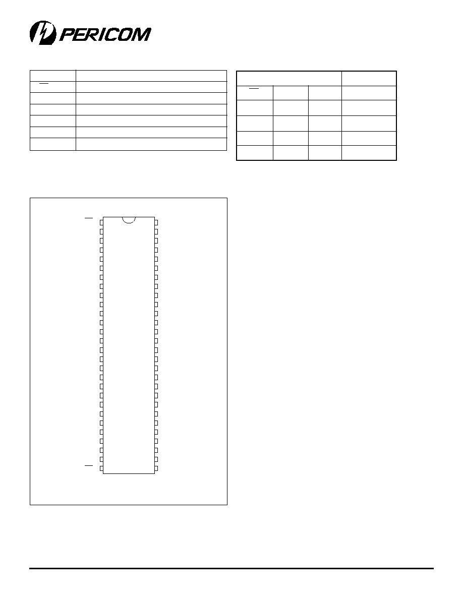
Pin Name
Description
OE
Output Enable Input (Active LOW)
CLK
Clock Input (Active HIGH)
Dx
Data Inputs
Qx
3-State Outputs
GND
Ground
V
CC
Power
1
2
3
4
5
6
7
8
9
10
11
12
13
14
15
16
17
18
19
20
21
22
23
24
56
55
54
53
52
51
50
49
48
47
46
45
44
43
42
41
40
39
38
37
36
35
34
33
25
26
27
28
32
31
30
29
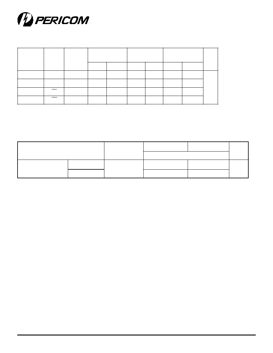
Product Pin Description
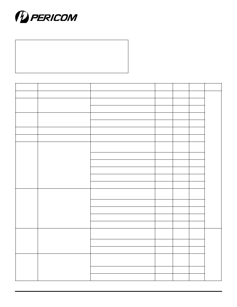
Truth Table
(1)
Note:
1. H = High Signal Level
L = Low Signal Level
X = Irrelevant
Z = High Impedance
= LOW-to-HIGH Transition
n = 1,2
Product Pin Configuration
56-PIN
V56
A56
1OE
1Q1
1Q2
GND
2Q1
2Q2
VCC
3Q1
3Q2
4Q1
GND
4Q2
5Q1
5Q2
6Q1
6Q2
7Q1
GND
7Q2
8Q1
8Q2
VCC
9Q1
9Q2
GND
10Q1
10Q2
2OE
CLK
D1
NC
GND
D2
NC
VCC
D3
NC
D4
GND
NC
D5
NC
D6
NC
D7
GND
NC
D8
NC
VCC
D9
NC
GND
D10
NC
NC
s
t
u
p
n
I
s
t
u
p
t
u
O
n
E
O
K
L
C
D
n
Q
L
H
H
L
L
L
L
L
X
0
Q
H
X
X
Z
PI74ALVCH162820
3.3V 10-BIT FLIP-FLOP WITH
DUAL OUTPUTS AND 3-STATE OUTPUTS
3
PS8094A 03/26/97
12345678901234567890123456789012123456789012345678901234567890121234567890123456789012345678901212345678901234567890123456789012123456789012
DC Electrical Characteristics
(Over the Operating Range, T
A
= 40°C to +85°C, V
CC
= 3.3V ± 10%)
s
r
e
t
e
m
a
r
a
P
n
o
it
p
i
r
c
s
e
D
s
n
o
it
i
d
n
o
C
t
s
e
T
)
1
(
.
n
i
M
.
p
y
T
)
2
(
.
x
a
M
s
ti
n
U
V
C
C
e
g
a
tl
o
V
y
l
p
p
u
S
3
.
2
6
.
3
V
V
H
I
)
3
(
e
g
a
tl
o
V
H
G
I
H
t
u
p
n
I
V
C
C
V
7
.
2
o
t
V
3
.
2
=
7
.
1
V
C
C
V
6
.
3
o
t
V
7
.
2
=
0
.
2
V
L
I
)
3
(
e
g
a
tl
o
V
W
O
L
t
u
p
n
I
V
C
C
V
7
.
2
o
t
V
3
.
2
=
7
.
0
V
C
C
V
6
.
3
o
t
V
7
.
2
=
8
.
0
V
N
I
)
3
(
e
g
a
tl
o
V
t
u
p
n
I
0
V
C
C
V
T
U
O
)
3
(
e
g
a
tl
o
V
t
u
p
t
u
O
0
V
C
C
V
H
O
t
u
p
t
u
O
H
G
I
H
e
g
a
tl
o
V
I
H
O
0
0
1
-
=
m V
,
A
C
C
=
.
x
a
M
o
t
.
n
i
M
V
C
C
2
.
0
-
V
H
I
I
,
V
7
.
1
=
H
O
6
-
=
V
,
A
m
C
C
=
V
3
.
2
0
.
2
V
H
I
I
,
V
7
.
1
=
H
O
2
1
-
=
V
,
A
m
C
C
=
V
3
.
2
7
.
1
V
H
I
I
,
V
0
.
2
=
H
O
2
1
-
=
V
,
A
m
C
C
=
V
7
.
2
2
.
2
V
H
I
I
,
V
0
.
2
=
H
O
2
1
-
=
V
,
A
m
C
C
=
V
0
.
3
4
.
2
V
H
I
I
,
V
0
.
2
=
H
O
4
2
-
=
V
,
A
m
C
C
=
V
0
.
3
0
.
2
V
L
O
t
u
p
t
u
O
W
O
L
e
g
a
tl
o
V
I
L
O
0
0
1
=
m V
,
A
L
I
=
.
x
a
M
o
t
.
n
i
M
2
.
0
V
L
I
I
,
V
7
.
0
=
L
O
6
=
V
,
A
m
C
C
=
V
3
.
2
4
.
0
V
L
I
I
,
V
7
.
0
=
L
O
2
1
=
V
,
A
m
C
C
=
V
3
.
2
7
.
0
V
L
I
I
,
V
8
.
0
=
L
O
2
1
=
V
,
A
m
C
C
=
V
7
.
2
4
.
0
V
L
I
I
,
V
8
.
0
=
L
O
4
2
=
V
,
A
m
C
C
=
V
0
.
3
5
5
.
0
I
H
O
)
3
(
t
u
p
t
u
O
H
G
I
H
t
n
e
rr
u
C
V
C
C
V
3
.
2
=
2
1
-
A
m
V
C
C
V
7
.
2
=
2
1
-
V
C
C
V
0
.
3
=
4
2
-
I
L
O
)
3
(
t
u
p
t
u
O
W
O
L
t
n
e
rr
u
C
V
C
C
V
3
.
2
=
2
1
V
C
C
V
7
.
2
=
2
1
V
C
C
V
0
.
3
=
4
2
Storage Temperature ........................................................... 65°C to +150°C
Ambient Temperature with Power Applied ........................ 40°C to +85°C
Input Voltage Range, V
IN ......................................................
0.5V to V
CC
+0.5V
Output Voltage Range, V
OUT ...............................................
0.5V to V
CC
+0.5V
DC Input Voltage .................................................................... 0.5V to +5.0V
DC Output Current ............................................................................ 100 mA
Power Dissipation .................................................................................. 1.0W
Note:
Stresses greater than those listed under MAXIMUM RATINGS
may cause permanent damage to the device. This is a stress rating
only and functional operation of the device at these or any other
conditions above those indicated in the operational sections of this
specification is not implied. Exposure to absolute maximum rating
conditions for extended periods may affect reliability.
Maximum Ratings
(Above which the useful life may be impaired. For user guidelines, not tested.)
PI74ALVCH162820
3.3V 10-BIT FLIP-FLOP WITH
DUAL OUTPUTS AND 3-STATE OUTPUTS
4
PS8094A 03/26/97
12345678901234567890123456789012123456789012345678901234567890121234567890123456789012345678901212345678901234567890123456789012123456789012
Notes:
1. For conditions shown as Max. or Min., use appropriate value specified under Electrical Characteristics for the applicable device type.
2. Typical values are at V
CC
= 3.3V, +25°C ambient and maximum loading.
3. Unused Control Inputs must be held HIGH or LOW to prevent them from floating.
DC Electrical Characteristics-
Continued (Over the Operating Range, T
A
= 40°C to +85°C, V
CC
= 3.3V ±10%)
s
r
e
t
e
m
a
r
a
P
n
o
it
p
i
r
c
s
e
D
s
n
o
it
i
d
n
o
C
t
s
e
T
)
1
(
.
n
i
M
.
p
y
T
)
2
(
.
x
a
M
s
ti
n
U
I
N
I
t
n
e
rr
u
C
t
u
p
n
I
V
N
I
V
=
C
C
V
,
D
N
G
r
o
C
C
V
6
.
3
=
5
±
mA
I
N
I
(
HOLD
)
t
u
p
n
I
d
l
o
H
t
n
e
rr
u
C
V
N
I
V
,
V
7
.
0
=
C
C
V
3
.
2
=
5
4
V
N
I
V
,
V
7
.
1
=
C
C
V
3
.
2
=
5
4
-
V
N
I
V
,
V
8
.
0
=
C
C
V
0
.
3
=
5
7
V
N
I
V
,
V
0
.
2
=
C
C
V
0
.
3
=
5
7
-
V
N
I
0
=
o
t
V
,
V
6
.
3
C
C
V
6
.
3
=
0
0
5
±
I
Z
O
)
st
u
p
t
u
O
E
T
A
T
S
-
3
(
t
n
e
rr
u
C
t
u
p
t
u
O
V
T
U
O
V
=
C
C
r
o
,
D
N
G
V
C
C
V
6
.
3
=
0
1
±
I
C
C
t
n
e
rr
u
C
y
l
p
p
u
S
V
C
C
=
V
6
.
3
I
,
T
U
O
0
= m ,
A
V
N
I
V
r
o
D
N
G
=
C
C
0
4
DI
C
C
t
u
p
n
I
r
e
p
t
n
e
rr
u
C
y
l
p
p
u
S
H
G
I
H
L
T
T
@
V
C
C
V
0
.
3
=
o
t
6
.
3 V
V
t
a
t
u
p
n
I
e
n
O
C
C
-
V
6
.
0
V
t
a
st
u
p
n
I
r
e
h
t
O
C
C
D
N
G
r
o
0
5
7
C
I
st
u
p
n
I
l
o
rt
n
o
C
V
N
I
V
=
C
C
V
,
D
N
G
r
o
C
C
V
3
.
3
=
5
.
3
F
p
st
u
p
n
I
a
t
a
D
6
C
O
st
u
p
t
u
O
V
O
V
=
C
C
V
,
D
N
G
r
o
C
C
V
3
.
3
=
7
Timing Requirements over Operating Range
s
r
e
t
e
m
a
r
a
P
n
o
it
p
i
r
c
s
e
D
V
C
C
V
2
.
0
±
V
5
.
2
=
V
C
C
V
7
.
2
=
V
C
C
V
3
.
0
±
V
3
.
3
=
s
ti
n
U
.
n
i
M
.
x
a
M
.
n
i
M
.
x
a
M
.
n
i
M
.
x
a
M
f
K
C
O
L
C
0
0
5
1
0
0
5
1
0
0
5
1
z
H
M
t
W
K
L
C
n
o
it
a
r
u
d
e
sl
u
P
W
O
L
r
o
H
G
I
H
3
.
3
3
.
3
3
.
3
s
n
t
U
S
K
L
C
e
r
o
f
e
b
a
t
a
d
,
e
m
it
p
u
t
e
S
7
.
1
8
.
1
4
.
1
t
H
K
L
C
r
e
tf
a
a
t
a
d
,
e
m
it
d
l
o
H
1
.
1
1
.
1
0
.
1
D /tDv
)
3
(
ll
a
F
r
o
e
si
R
n
o
it
i
s
n
a
r
T
t
u
p
n
I
0
0
1
0
0
1
0
0
1
V
/
s
n
Note:
1. Unused control inputs must be held HIGH or LOW to prevent them from floating.
PI74ALVCH162820
3.3V 10-BIT FLIP-FLOP WITH
DUAL OUTPUTS AND 3-STATE OUTPUTS
5
PS8094A 03/26/97
12345678901234567890123456789012123456789012345678901234567890121234567890123456789012345678901212345678901234567890123456789012123456789012
Notes:
1. See test circuit and wave forms.
2. Minimum limits are guaranteed but not tested on Propagation Delays.
Switching Characteristics over Operating Range
(1)
s
r
e
t
e
m
a
r
a
P
m
o
r
F
)
T
U
P
N
I
(
o
T
)
T
U
P
T
U
O
(
V
C
C
V
2
.
0
±
V
5
.
2
=
V
C
C
V
7
.
2
=
V
C
C
V
3
.
0
±
V
3
.
3
=
s
ti
n
U
.
n
i
M
)
2
(
.
x
a
M
.
n
i
M
)
2
(
.
x
a
M
.
n
i
M
)
2
(
.
x
a
M
)
2
(
f
X
A
M
0
5
1
0
5
1
0
5
1
s
n
t
D
P
K
L
C
Q
0
.
1
0
.
7
2
.
6
0
.
1
4
.
5
t
N
E
E
O
Q
0
.
1
4
.
7
8
.
6
0
.
1
6
.
5
t
S
I
D
E
O
Q
3
.
1
4
.
6
5
.
5
0
.
1
0
.
5
Pericom Semiconductor Corporation
2380 Bering Drive · San Jose, CA 95131 · 1-800-435-2336 · Fax (408) 435-1100 · http://www.pericom.com
Operating Characteristics, T
A
= 25ºC
r
e
t
e
m
a
r
a
P
s
n
o
it
i
d
n
o
C
t
s
e
T
V
C
C
V
2
.
0
±
V
5
.
2
=
V
C
C
V
3
.
0
±
V
3
.
3
=
s
ti
n
U
l
a
c
i
p
y
T
C
D
P
n
o
it
a
p
i
s
si
D
r
e
w
o
P
e
c
n
a
ti
c
a
p
a
C
d
el
b
a
n
E
st
u
p
t
u
O
C
L
,
F
p
0
5
=
z
H
M
0
1
=
f
8
6
6
6
F
p
d
el
b
a
si
D
st
u
p
t
u
O
9
3
7
4