1
PS8093B 10/09/00
12345678901234567890123456789012123456789012345678901234567890121234567890123456789012345678901212345678901234567890123456789012123456789012
12345678901234567890123456789012123456789012345678901234567890121234567890123456789012345678901212345678901234567890123456789012123456789012
12345678901234567890123456789012123456789012345678901234567890121234567890123456789012345678901212345678901234567890123456789012123456789012
16-Bit Transparent D-Type Latch
with 3-STATE Outputs
PI74ALVCH16373
Product Description
Pericom Semiconductor's PI74ALVCH series of logic circuits are
produced in the Company's advanced 0.5 micron CMOS
technology, achieving industry leading speed.
This 16-bit transparent D-type latch is designed for 2.3V to 3.6V
V
CC
operation.
The PI74ALVCH16373 is particularly suitable for implementing
buffer registers, I/O ports, bidirectional bus drivers, and working
registers. This device can be used as two 8-bit latches or one 16-bit
latch. When the Latch Enable (LE) input is HIGH, the Q outputs
follow the (D) inputs. When LE is taken LOW, the Q outputs are
latched at the levels set up at the D inputs.
A buffered Output Enable (OE) input can be used to place the
eight outputs in either a normal logic state (high or low logic
levels) or a high-impedance state in which the outputs neither
load nor drive the bus lines significantly. The high-impedance state
and the increased drive provide the capability to drive bus lines
without need for interface or pullup components. OE does not
affect internal operations of the latch. Old data can be retained
or new data can be entered while the outputs are in the high
impedance state.
To ensure the high impedance state during power up or power
down, OE should be tied to V
CC
through a pullup resistor; the
minimum value of the resistor is determined by the current-sinking
capability of the driver.
Active bus-hold circuitry is provided to hold unused or floating
data inputs at a valid logic level.
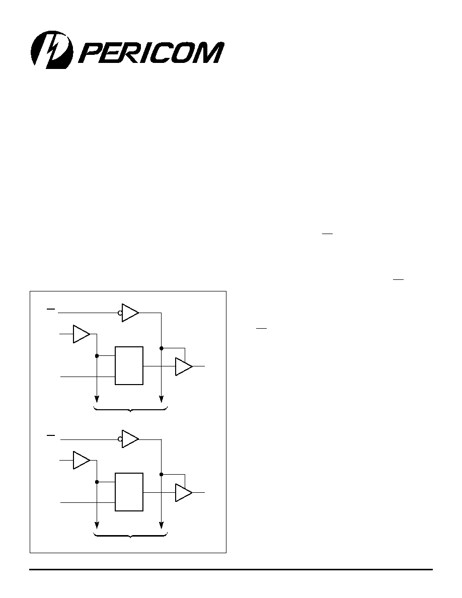
1LE
1Q1
1D
C1
1D1
To Seven Other Channels
1OE
1
48
47
2
2LE
2Q1
1D
C1
2D1
To Seven Other Channels
25
36
13
24
2OE
Product Features
�
PI74ALVCH16373 is designed for low voltage operation
�
V
CC
= 2.3V to 3.6V
�
Hysteresis on all inputs
�
Typical V
OLP
(Output Ground Bounce)
< 0.8V at V
CC
= 3.3V, T
A
= 25�C
�
Typical V
OHV
(Output V
OH
Undershoot)
< 2.0V at V
CC
= 3.3V, T
A
= 25�C
�
Bus Hold retains last active bus state during 3-STATE,
eliminating the need for external pullup resistors
�
Industrial operation at �40�C to +85�C
�
Packages available:
� 48-pin 240 mil wide plastic TSSOP (A)
� 48-pin 300 mil wide plastic SSOP (V)
Logic Block Diagram
2
PS8093B 10/09/00
12345678901234567890123456789012123456789012345678901234567890121234567890123456789012345678901212345678901234567890123456789012123456789012
12345678901234567890123456789012123456789012345678901234567890121234567890123456789012345678901212345678901234567890123456789012123456789012
PI74ALVCH16373
16-Bit Transparent D-Type Latch
with 3-STATE Outputs
s
t
u
p
n
I
s
t
u
p
t
u
O
E
O
E
L
D
Q
L
H
H
H
L
H
L
L
L
L
X
Q
0
H
X
X
Z
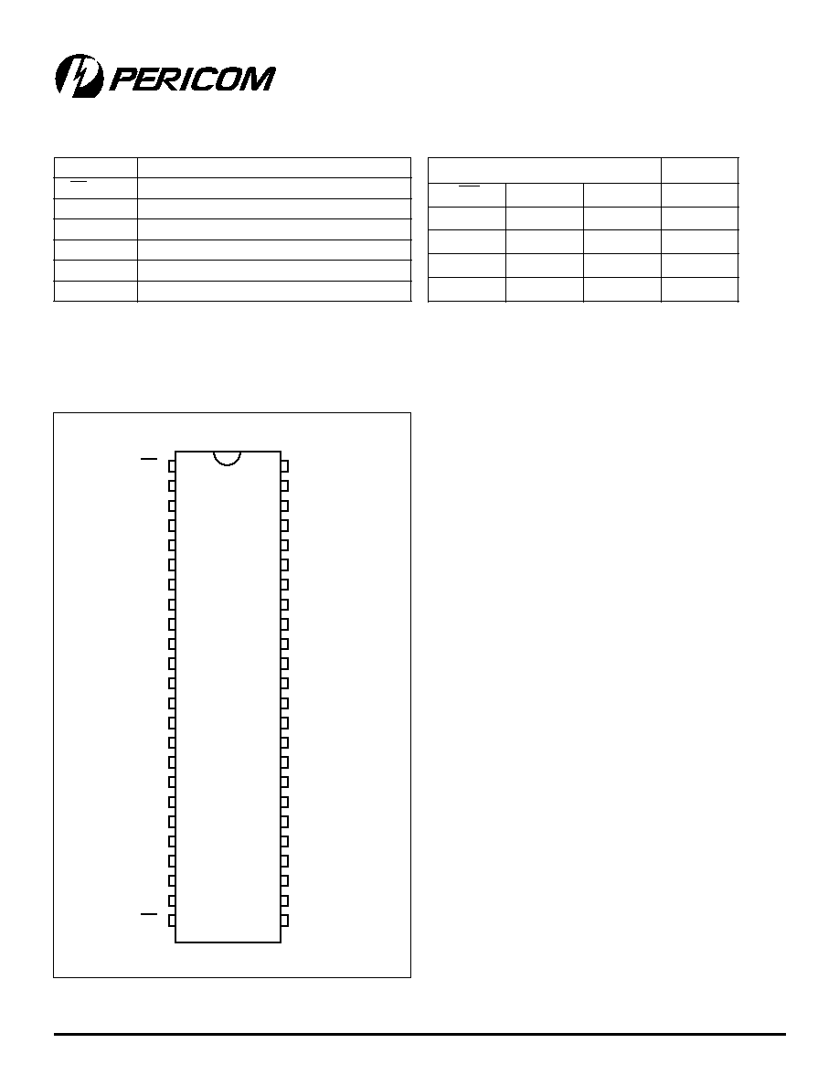
Pin Name
Description
OE
Output Enable Input (Active LOW)
LE
Latch Enable (Active HIGH)
Dx
Data Inputs
Qx
3-State Outputs
GND
Ground
V
CC
Power
Product Pin Description
Truth Table
(1)
Product Pin Configuration
Notes:
1. H = High Signal Level
L = Low Signal Level
X = Irrelevant
Z = High Impedance
1
2
3
4
5
6
7
8
9
48
10
47
11
46
12
45
13
44
14
43
15
42
16
41
17
40
18
39
19
38
20
37
21
36
22
35
23
34
24
33
32
31
30
29
28
27
26
25
1OE
1LE
1Q1
1D1
1Q2
1D2
GND
GND
1Q3
1D3
1Q4
1D4
V
1Q5
1D5
1Q6
1D6
GND
GND
1Q7
1D7
1Q8
1D8
2Q1
2D1
2Q2
2D2
GND
GND
2Q3
2D3
2Q4
2D4
2Q5
2D5
2Q6
2D6
GND
GND
2Q7
2D7
2Q8
2D8
2OE
2LE
CC
VCC
VCC
VCC
48-Pin
V,A
PI74ALVCH16373
16-Bit Transparent D-Type Latch
with 3-STATE Outputs
3
PS8093B 10/09/00
12345678901234567890123456789012123456789012345678901234567890121234567890123456789012345678901212345678901234567890123456789012123456789012
Storage Temperature ............................................................ �65�C to +150�C
Ambient Temperature with Power Applied .......................... �40�C to +85�C
Input Voltage Range, V
IN ....................................................
�0.5V to V
CC
+0.5V
Output Voltage Range, V
OUT .............................................
�0.5V to V
CC
+0.5V
DC Input Voltage ................................................................... �0.5V to +5.0V
DC Output Current .............................................................................. 100 mA
Power Dissipation ................................................................................... 1.0W
Note:
Stresses greater than those listed under MAXIMUM RATINGS
may cause permanent damage to the device. This is a stress rating
only and functional operation of the device at these or any other
conditions above those indicated in the operational sections of
this specification is not implied. Exposure to absolute maximum
rating conditions for extended periods may affect reliability.
DC Electrical Characteristics
(Over the Operating Range, T
A
= �40�C to +85�C, V
CC
= 3.3V �10%)
Maximum Ratings
(Above which the useful life may be impaired. For user guidelines, not tested.)
s
r
e
t
e
m
a
r
a
P
n
o
i
t
p
i
r
c
s
e
D
s
n
o
i
t
i
d
n
o
C
t
s
e
T
)
1
(
.
n
i
M
.
p
y
T
)
2
(
.
x
a
M
s
t
i
n
U
V
C
C
e
g
a
t
l
o
V
y
l
p
p
u
S
3
.
2
6
.
3
V
V
H
I
)
3
(
e
g
a
t
l
o
V
H
G
I
H
t
u
p
n
I
V
C
C
V
7
.
2
o
t
V
3
.
2
=
7
.
1
V
C
C
V
6
.
3
o
t
V
7
.
2
=
0
.
2
V
L
I
)
3
(
e
g
a
t
l
o
V
W
O
L
t
u
p
n
I
V
C
C
V
7
.
2
o
t
V
3
.
2
=
7
.
0
V
C
C
V
6
.
3
o
t
V
7
.
2
=
8
.
0
V
N
I
)
3
(
e
g
a
t
l
o
V
t
u
p
n
I
0
V
C
C
V
T
U
O
)
3
(
e
g
a
t
l
o
V
t
u
p
t
u
O
0
V
C
C
V
H
O
t
u
p
t
u
O
H
G
I
H
e
g
a
t
l
o
V
I
H
O
0
0
1
-
=
�
V
,
A
C
C
=
.
x
a
M
o
t
.
n
i
M
V
C
C
2
.
0
-
V
H
I
I
,
V
7
.
1
=
H
O
6
-
=
V
,
A
m
C
C
=
V
3
.
2
0
.
2
V
H
I
I
,
V
7
.
1
=
H
O
2
1
-
=
V
,
A
m
C
C
=
V
3
.
2
7
.
1
V
H
I
I
,
V
0
.
2
=
H
O
2
1
-
=
V
,
A
m
C
C
=
V
7
.
2
2
.
2
V
H
I
I
,
V
0
.
2
=
H
O
2
1
-
=
V
,
A
m
C
C
=
V
0
.
3
4
.
2
V
H
I
I
,
V
0
.
2
=
H
O
4
2
-
=
V
,
A
m
C
C
=
V
0
.
3
0
.
2
V
L
O
t
u
p
t
u
O
W
O
L
e
g
a
t
l
o
V
I
L
O
0
0
1
=
�
V
,
A
L
I
=
.
x
a
M
o
t
.
n
i
M
2
.
0
V
L
I
I
,
V
7
.
0
=
L
O
6
=
V
,
A
m
C
C
=
V
3
.
2
4
.
0
V
L
I
I
,
V
7
.
0
=
L
O
2
1
=
V
,
A
m
C
C
=
V
3
.
2
7
.
0
V
L
I
I
,
V
8
.
0
=
L
O
2
1
=
V
,
A
m
C
C
=
V
7
.
2
4
.
0
V
L
I
I
,
V
8
.
0
=
L
O
4
2
=
V
,
A
m
C
C
=
V
0
.
3
5
5
.
0
I
H
O
)
3
(
t
u
p
t
u
O
H
G
I
H
t
n
e
r
r
u
C
V
C
C
V
3
.
2
=
2
1
-
A
m
V
C
C
V
7
.
2
=
2
1
-
V
C
C
V
0
.
3
=
4
2
-
I
L
O
)
3
(
t
u
p
t
u
O
W
O
L
t
n
e
r
r
u
C
V
C
C
V
3
.
2
=
2
1
V
C
C
V
7
.
2
=
2
1
V
C
C
V
0
.
3
=
4
2
4
PS8093B 10/09/00
12345678901234567890123456789012123456789012345678901234567890121234567890123456789012345678901212345678901234567890123456789012123456789012
12345678901234567890123456789012123456789012345678901234567890121234567890123456789012345678901212345678901234567890123456789012123456789012
PI74ALVCH16373
16-Bit Transparent D-Type Latch
with 3-STATE Outputs
Notes:
1. For conditions shown as Max. or Min., use appropriate value specified under Electrical Characteristics for the applicable device type.
2. Typical values are at V
CC
= 3.3V, +25�C ambient and maximum loading.
3. Unused Control Inputs must be held HIGH or LOW to prevent them from floating.
DC Electrical Characteristics-
Continued (Over the Operating Range, T
A
= �40�C to +85�C, V
CC
= 3.3V �10%)
s
r
e
t
e
m
a
r
a
P
n
o
i
t
p
i
r
c
s
e
D
s
n
o
i
t
i
d
n
o
C
t
s
e
T
)
1
(
.
n
i
M
.
p
y
T
)
2
(
.
x
a
M
s
t
i
n
U
I
N
I
t
n
e
r
r
u
C
t
u
p
n
I
V
N
I
V
=
C
C
V
,
D
N
G
r
o
C
C
V
6
.
3
=
5
�
�
A
I
N
I
(
HOLD
)
t
u
p
n
I
d
l
o
H
t
n
e
r
r
u
C
V
N
I
V
,
V
7
.
0
=
C
C
V
3
.
2
=
5
4
V
N
I
V
,
V
7
.
1
=
C
C
V
3
.
2
=
5
4
-
V
N
I
V
,
V
8
.
0
=
C
C
V
0
.
3
=
5
7
V
N
I
V
,
V
0
.
2
=
C
C
V
0
.
3
=
5
7
-
V
N
I
0
=
o
t
V
,
V
6
.
3
C
C
V
6
.
3
=
0
0
5
�
I
Z
O
)
s
t
u
p
t
u
O
E
T
A
T
S
-
3
(
t
n
e
r
r
u
C
t
u
p
t
u
O
V
T
U
O
V
=
C
C
r
o
,
D
N
G
V
C
C
V
6
.
3
=
0
1
�
I
C
C
t
n
e
r
r
u
C
y
l
p
p
u
S
V
C
C
=
V
6
.
3
I
,
T
U
O
0
=
�
,
A
V
N
I
V
r
o
D
N
G
=
C
C
0
4
I
C
C
t
u
p
n
I
r
e
p
t
n
e
r
r
u
C
y
l
p
p
u
S
H
G
I
H
L
T
T
@
V
C
C
V
0
.
3
=
o
t
6
.
3 V
V
t
a
t
u
p
n
I
e
n
O
C
C
-
V
6
.
0
V
t
a
s
t
u
p
n
I
r
e
h
t
O
C
C
D
N
G
r
o
0
5
7
C
I
s
t
u
p
n
I
l
o
r
t
n
o
C
V
N
I
V
=
C
C
V
,
D
N
G
r
o
C
C
V
3
.
3
=
3
F
p
s
t
u
p
n
I
a
t
a
D
6
C
O
s
t
u
p
t
u
O
V
O
V
=
C
C
V
,
D
N
G
r
o
C
C
V
3
.
3
=
7
s
r
e
t
e
m
a
r
a
P
n
o
i
t
p
i
r
c
s
e
D
V
C
C
V
2
.
0
�
V
5
.
2
=
V
C
C
V
7
.
2
=
V
C
C
V
3
.
0
�
V
3
.
3
=
s
t
i
n
U
.
n
i
M
.
x
a
M
.
n
i
M
.
x
a
M
.
n
i
M
.
x
a
M
t
W
E
L
n
o
i
t
a
r
u
D
e
s
l
u
P
W
O
L
r
o
H
G
I
H
3
.
3
3
.
3
3
.
3
s
n
t
U
S
a
t
a
D
e
m
i
T
p
u
t
e
S
E
L
e
r
o
f
e
B
0
.
1
0
.
1
1
.
1
t
H
a
t
a
D
e
m
i
T
d
l
o
H
E
L
r
e
t
f
A
5
.
1
7
.
1
4
.
1
/
t
v
)
1
(
n
o
i
t
i
s
n
a
r
T
t
u
p
n
I
l
l
a
F
r
o
e
s
i
R
0
0
1
0
0
1
0
0
1
V
/
s
n
Timing Requirements over Operating Range
Note:
1. Unused control inputs must be held HIGH or LOW to prevent them from floating.
PI74ALVCH16373
16-Bit Transparent D-Type Latch
with 3-STATE Outputs
5
PS8093B 10/09/00
12345678901234567890123456789012123456789012345678901234567890121234567890123456789012345678901212345678901234567890123456789012123456789012
s
r
e
t
e
m
a
r
a
P
)
T
U
P
N
I
(
m
o
r
F
)
T
U
P
T
U
O
(
o
T
V
C
C
V
2
.
0
�
V
5
.
2
=
V
C
C
V
7
.
2
=
V
C
C
V
3
.
0
�
V
3
.
3
=
s
t
i
n
U
.
n
i
M
)
2
(
.
x
a
M
.
n
i
M
.
x
a
M
.
n
i
M
)
2
(
.
x
a
M
t
D
P
D
Q
0
.
1
5
.
4
3
.
4
1
.
1
6
.
3
s
n
t
D
P
E
L
0
.
1
9
.
5
6
.
4
0
.
1
9
.
3
t
N
E
E
O
0
.
1
0
.
6
7
.
5
0
.
1
7
.
4
t
S
I
D
E
O
9
.
1
1
.
5
5
.
4
4
.
1
1
.
4
Switching Characteristics over Operating Range
(1)
Pericom Semiconductor Corporation
2380 Bering Drive � San Jose, CA 95131 � 1-800-435-2336 � Fax (408) 435-1100 � http://www.pericom.com
Operating Characteristics, T
A
= 25�C
r
e
t
e
m
a
r
a
P
s
n
o
i
t
i
d
n
o
C
t
s
e
T
V
C
C
V
2
.
0
�
V
5
.
2
=
V
C
C
V
3
.
0
�
V
3
.
3
=
s
t
i
n
U
.
p
y
T
C
D
P
n
o
i
t
a
p
i
s
s
i
D
r
e
w
o
P
e
c
n
a
t
i
c
a
p
a
C
d
e
l
b
a
n
E
s
t
u
p
t
u
O
C
L
z
H
M
0
1
=
f
,
F
p
0
5
=
9
1
2
2
F
p
d
e
l
b
a
s
i
D
s
t
u
p
t
u
O
4
5
Notes:
1. See test circuit and waveforms.
2. Minimum limits are guaranteed but not tested on Propagation Delays.