1
PS8091A 03/26/97
12345678901234567890123456789012123456789012345678901234567890121234567890123456789012345678901212345678901234567890123456789012123456789012
12345678901234567890123456789012123456789012345678901234567890121234567890123456789012345678901212345678901234567890123456789012123456789012
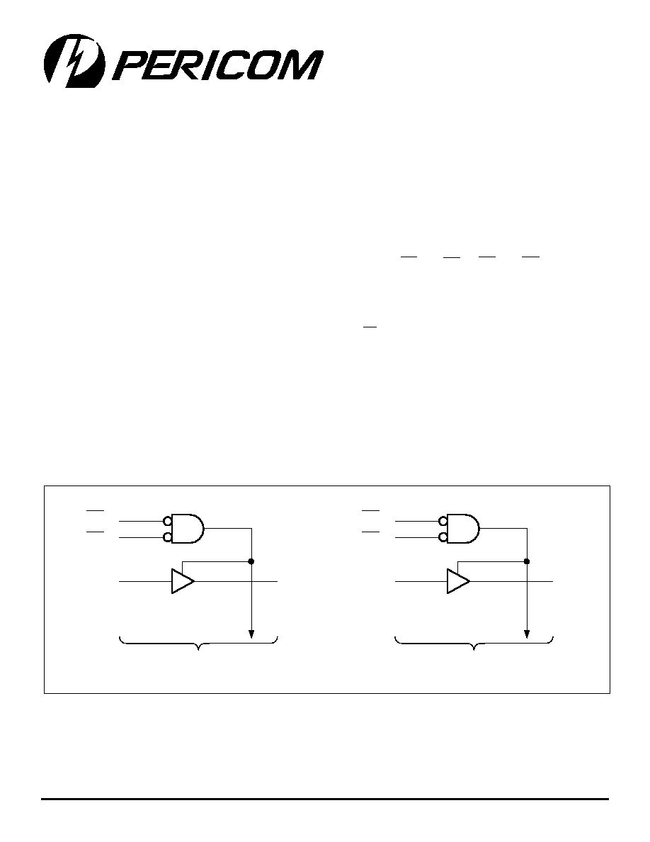
Logic Block Diagram
Product Description
Pericom Semiconductor's PI74ALVCH series of logic circuits are
produced in the Company's advanced 0.5 micron CMOS technology,
achieving industry leading speed grades.
The PI74ALVCH16827 is a 20-bit non-inverting buffer/driver
designed for 2.3V to 3.6V Vcc operation.
The buffer/driver is composed of two 10-bit sections with separate
output-enable signals. For either 10-bit buffer section, the two
output-enable (1OE1 and 1OE2 or 2OE1 and 2OE2 inputs must both
be low for the corresponding Y outputs to be active. If either output-
enable input is HIGH, the outputs of that 10-bit buffer section are
in the high-impedance state.
To ensure the high-impedance state during power up or power
down, OE should be tied to Vcc through a pull-up resistor; the
minimum value of the resistor is determined by the current sinking
ability of the driver.
The PI74ALVCH16827 has the "Bus Hold" which retains the data
input's last state whenever the data input goes to high-impedance
preventing `floating" inputs and eliminating the need for pullup/
down resistors.
PI74ALVCH16827
20-Bit Buffer/Driver
with 3-STATE Outputs
1
OE
1
1
OE
2
1
A
1
1
Y
1
To 9 other channels
1
56
55
2
2
OE
1
2
OE
2
2
A
1
2
Y
1
To 9 other channels
28
29
42
15
Product Features
�
PI74ALVCH16827 is designed for low voltage operation
�
V
CC
= 2.3V to 3.6V
�
Hysteresis on all inputs
�
Typical V
OLP
(Output Ground Bounce)
< 0.8V at V
CC
= 3.3V, T
A
= 25�C
�
Typical V
OHV
(Output V
OH
Undershoot)
< 2.0V at V
CC
= 3.3V, T
A
= 25�C
�
Bus Hold retains last active bus state during 3-STATE,
eliminating the need for external pullup resistors
�
Industrial operation at 40�C to +85�C
�
Packages available:
56-pin 240 mil wide plastic TSSOP (A)
56-pin 300 mil wide plastic SSOP (V)

PI74ALVCH16827
20-BIT BUFFER/DRIVER WITH 3-STATE OUTPUTS
2
PS8091A 03/26/97
12345678901234567890123456789012123456789012345678901234567890121234567890123456789012345678901212345678901234567890123456789012123456789012
e
m
a
N
n
i
P
n
o
it
p
i
r
c
s
e
D
OE
)
W
O
L
e
v
it
c
A
(
st
u
p
n
I
el
b
a
n
E
t
u
p
t
u
O
A
X
st
u
p
n
I
a
t
a
D
Y
X
st
u
p
t
u
O
e
t
a
t
S
-
3
D
N
G
d
n
u
o
r
G
V
CC
r
e
w
o
P
Product Pin Description
Truth Table
(1)
Note:
1. H = High Signal Level
L = Low Signal Level
X = Irrelevant
Z = High Impedance
Product Pin Configuration
s
t
u
p
n
I
s
t
u
p
t
u
O
1
E
O
2
E
O
A
Y
L
L
L
L
L
L
H
H
H
X
X
Z
X
H
X
Z
1
2
3
4
5
6
7
8
9
10
11
12
13
14
15
16
17
18
19
20
21
22
23
24
56
55
54
53
52
51
50
49
48
47
46
45
44
43
42
41
40
39
38
37
36
35
34
33
25
26
27
28
32
31
30
29
1
OE
2
1
A
1
1
A
2
GND
1
A
3
1
A
4
V
CC
1
A
5
1
A
6
1
A
7
GND
1
A
8
1
A
9
1
A
10
2
A
1
2
A
2
2
A
3
GND
2
A
4
2
A
5
2
A
6
V
CC
2
A
7
2
A
8
GND
2
A
9
2
A
10
2
OE
2
56-PIN
V56
A56
1
OE
1
1
Y
1
1
Y
2
GND
1
Y
3
1
Y
4
V
CC
1
Y
5
1
Y
6
1
Y
7
GND
1
Y
8
1
Y
9
1
Y
10
2
Y
1
2
Y
2
2
Y
3
GND
2
Y
4
2
Y
5
2
Y
6
V
CC
2
Y
7
2
Y
8
GND
2
Y
9
2
Y
10
2
OE
1

3
PS8091A 03/26/97
12345678901234567890123456789012123456789012345678901234567890121234567890123456789012345678901212345678901234567890123456789012123456789012
PI74ALVCH16827
20-BIT BUFFER/DRIVER WITH 3-STATE OUTPUTS
DC Electrical Characteristics
(Over the Operating Range, T
A
= �40�C to +85�C, V
CC
= 3.3V � 10%)
s
r
e
t
e
m
a
r
a
P
n
o
it
p
i
r
c
s
e
D
s
n
o
it
i
d
n
o
C
t
s
e
T
)
1
(
.
n
i
M
.
p
y
T
)
2
(
.
x
a
M
s
ti
n
U
V
C
C
e
g
a
tl
o
V
y
l
p
p
u
S
3
.
2
6
.
3
V
V
H
I
)
3
(
e
g
a
tl
o
V
H
G
I
H
t
u
p
n
I
V
C
C
V
7
.
2
o
t
V
3
.
2
=
7
.
1
V
C
C
V
6
.
3
o
t
V
7
.
2
=
0
.
2
V
L
I
)
3
(
e
g
a
tl
o
V
W
O
L
t
u
p
n
I
V
C
C
V
7
.
2
o
t
V
3
.
2
=
7
.
0
V
C
C
V
6
.
3
o
t
V
7
.
2
=
8
.
0
V
N
I
)
3
(
e
g
a
tl
o
V
t
u
p
n
I
0
V
C
C
V
T
U
O
)
3
(
e
g
a
tl
o
V
t
u
p
t
u
O
0
V
C
C
V
H
O
t
u
p
t
u
O
H
G
I
H
e
g
a
tl
o
V
I
H
O
0
0
1
-
=
m V
,
A
C
C
=
.
x
a
M
o
t
.
n
i
M
V
C
C
2
.
0
-
V
H
I
I
,
V
7
.
1
=
H
O
6
-
=
V
,
A
m
C
C
=
V
3
.
2
0
.
2
V
H
I
I
,
V
7
.
1
=
H
O
2
1
-
=
V
,
A
m
C
C
=
V
3
.
2
7
.
1
V
H
I
I
,
V
0
.
2
=
H
O
2
1
-
=
V
,
A
m
C
C
=
V
7
.
2
2
.
2
V
H
I
I
,
V
0
.
2
=
H
O
2
1
-
=
V
,
A
m
C
C
=
V
0
.
3
4
.
2
V
H
I
I
,
V
0
.
2
=
H
O
4
2
-
=
V
,
A
m
C
C
=
V
0
.
3
0
.
2
V
L
O
t
u
p
t
u
O
W
O
L
e
g
a
tl
o
V
I
L
O
0
0
1
=
m V
,
A
L
I
=
.
x
a
M
o
t
.
n
i
M
2
.
0
V
L
I
I
,
V
7
.
0
=
L
O
6
=
V
,
A
m
C
C
=
V
3
.
2
4
.
0
V
L
I
I
,
V
7
.
0
=
L
O
2
1
=
V
,
A
m
C
C
=
V
3
.
2
7
.
0
V
L
I
I
,
V
8
.
0
=
L
O
2
1
=
V
,
A
m
C
C
=
V
7
.
2
4
.
0
V
L
I
I
,
V
8
.
0
=
L
O
4
2
=
V
,
A
m
C
C
=
V
0
.
3
5
5
.
0
I
H
O
)
3
(
t
u
p
t
u
O
H
G
I
H
t
n
e
rr
u
C
V
C
C
V
3
.
2
=
2
1
-
A
m
V
C
C
V
7
.
2
=
2
1
-
V
C
C
V
0
.
3
=
4
2
-
I
L
O
)
3
(
t
u
p
t
u
O
W
O
L
t
n
e
rr
u
C
V
C
C
V
3
.
2
=
2
1
V
C
C
V
7
.
2
=
2
1
V
C
C
V
0
.
3
=
4
2
Storage Temperature ........................................................... 65�C to +150�C
Ambient Temperature with Power Applied ........................ 40�C to +85�C
Input Voltage Range, V
IN ......................................................
0.5V to V
CC
+0.5V
Output Voltage Range, V
OUT ...............................................
0.5V to V
CC
+0.5V
DC Input Voltage .................................................................... 0.5V to +5.0V
DC Output Current ............................................................................ 100 mA
Power Dissipation .................................................................................. 1.0W
Note:
Stresses greater than those listed under MAXIMUM RATINGS
may cause permanent damage to the device. This is a stress rating
only and functional operation of the device at these or any other
conditions above those indicated in the operational sections of this
specification is not implied. Exposure to absolute maximum rating
conditions for extended periods may affect reliability.
Maximum Ratings
(Above which the useful life may be impaired. For user guidelines, not tested.)
PI74ALVCH16827
20-BIT BUFFER/DRIVER WITH 3-STATE OUTPUTS
4
PS8091A 03/26/97
12345678901234567890123456789012123456789012345678901234567890121234567890123456789012345678901212345678901234567890123456789012123456789012
s
r
e
t
e
m
a
r
a
P
m
o
r
F
)
T
U
P
N
I
(
o
T
)
T
U
P
T
U
O
(
V
C
C
V
2
.
0
�
V
5
.
2
=
V
C
C
V
7
.
2
=
V
C
C
V
3
.
0
�
V
3
.
3
=
s
ti
n
U
.
n
i
M
)
2
(
.
x
a
M
.
n
i
M
)
2
(
.
x
a
M
.
n
i
M
)
2
(
.
x
a
M
)
2
(
t
D
P
A
Y
0
.
1
7
.
4
9
.
3
0
.
1
4
.
3
z
H
M
t
N
E
E
O
0
.
1
5
.
6
7
.
5
0
.
1
7
.
4
s
n
t
S
I
D
E
O
9
.
1
8
.
5
9
.
4
3
.
1
5
.
4
D /tDv
)
1
(
ll
a
F
r
o
e
si
R
n
o
it
i
s
n
a
r
T
0
0
1
0
0
1
0
0
1
V
/
s
n
Notes:
1. For conditions shown as Max. or Min., use appropriate value specified under Electrical Characteristics for the applicable device type.
2. Typical values are at V
CC
= 3.3V, +25�C ambient and maximum loading.
3. Unused Control Inputs must be held HIGH or LOW to prevent them from floating.
DC Electrical Characteristics-
Continued (Over the Operating Range, T
A
= 40�C to +85�C, V
CC
= 3.3V �10%)
s
r
e
t
e
m
a
r
a
P
n
o
it
p
i
r
c
s
e
D
s
n
o
it
i
d
n
o
C
t
s
e
T
)
1
(
.
n
i
M
.
p
y
T
)
2
(
.
x
a
M
s
ti
n
U
I
N
I
t
n
e
rr
u
C
t
u
p
n
I
V
N
I
V
=
C
C
V
,
D
N
G
r
o
C
C
V
6
.
3
=
5
�
mA
I
N
I
(
HOLD
)
t
u
p
n
I
d
l
o
H
t
n
e
rr
u
C
V
N
I
V
,
V
7
.
0
=
C
C
V
3
.
2
=
5
4
V
N
I
V
,
V
7
.
1
=
C
C
V
3
.
2
=
5
4
-
V
N
I
V
,
V
8
.
0
=
C
C
V
0
.
3
=
5
7
V
N
I
V
,
V
0
.
2
=
C
C
V
0
.
3
=
5
7
-
V
N
I
0
=
o
t
V
,
V
6
.
3
C
C
V
6
.
3
=
0
0
5
�
I
Z
O
)
st
u
p
t
u
O
E
T
A
T
S
-
3
(
t
n
e
rr
u
C
t
u
p
t
u
O
V
T
U
O
V
=
C
C
r
o
,
D
N
G
V
C
C
V
6
.
3
=
0
1
�
I
C
C
t
n
e
rr
u
C
y
l
p
p
u
S
V
C
C
=
V
6
.
3
I
,
T
U
O
0
= m ,
A
V
N
I
V
r
o
D
N
G
=
C
C
0
4
DI
C
C
t
u
p
n
I
r
e
p
t
n
e
rr
u
C
y
l
p
p
u
S
H
G
I
H
L
T
T
@
V
C
C
V
0
.
3
=
o
t
6
.
3 V
V
t
a
t
u
p
n
I
e
n
O
C
C
-
V
6
.
0
V
t
a
st
u
p
n
I
r
e
h
t
O
C
C
D
N
G
r
o
0
5
7
C
I
st
u
p
n
I
l
o
rt
n
o
C
V
N
I
V
=
C
C
V
,
D
N
G
r
o
C
C
V
3
.
3
=
5
.
3
F
p
st
u
p
n
I
a
t
a
D
6
C
O
st
u
p
t
u
O
V
O
V
=
C
C
V
,
D
N
G
r
o
C
C
V
3
.
3
=
5
.
7
Notes:
1. See test circuit and wave forms.
2. Minimum limits are guaranteed but not tested on Propagation Delays.
Switching Characteristics over Operating Range
(1)
Pericom Semiconductor Corporation
2380 Bering Drive � San Jose, CA 95131 � 1-800-435-2336 � Fax (408) 435-1100 � http://www.pericom.com
Operating Characteristics, T
A
= 25�C
r
e
t
e
m
a
r
a
P
s
n
o
it
i
d
n
o
C
t
s
e
T
V
C
C
V
2
.
0
�
V
5
.
2
=
V
C
C
V
3
.
0
�
V
3
.
3
=
s
ti
n
U
l
a
c
i
p
y
T
C
D
P
n
o
it
a
p
i
s
si
D
r
e
w
o
P
e
c
n
a
ti
c
a
p
a
C
d
el
b
a
n
E
st
u
p
t
u
O
C
L
,
F
p
0
5
=
z
H
M
0
1
=
f
6
1
8
1
F
p
d
el
b
a
si
D
st
u
p
t
u
O
4
6