
1
PS2091B 09/19/02
Product Description
Pericom Semiconductor's PI74LCX series of logic circuits are
produced using the Company's advanced 0.6 micron CMOS
technology, achieving industry leading speed grades.
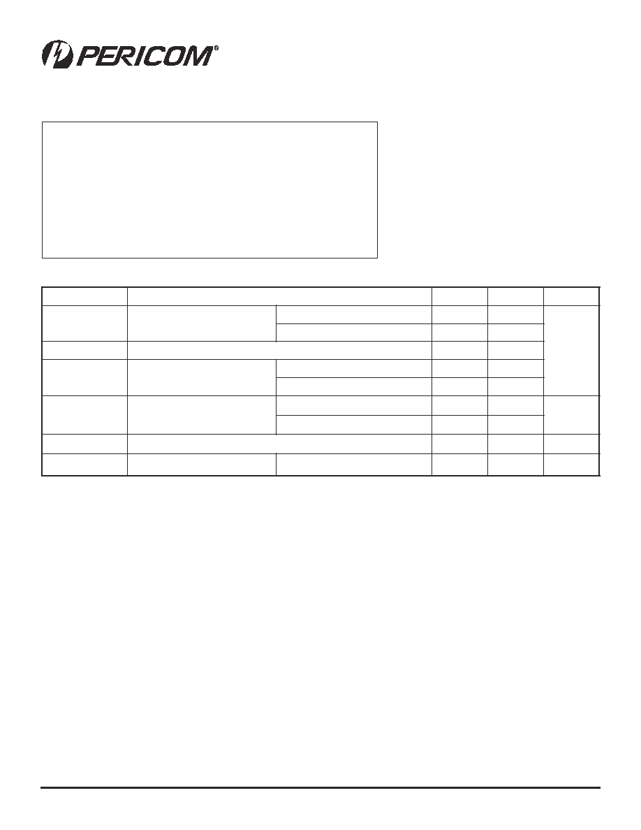
The PI74LCX16501 is an 18-bit registered bus transceiver designed
with D-type latches and flip-flops to allow data flow in transparent,
latched, and clocked modes. The Output Enable (OEAB and
OEBA, Latch Enable (LEAB and LEBA) and Clock (CLKAB and
CLKBA) inputs control the data flow in each direction. When
LEAB is HIGH, the device operates in transparent mode for A-to-
B data flow. When LEAB is LOW, the A data is latched if CLKAB
is held at a HIGH or LOW logic level. The A bus data is stored in
the latch/flip-flop on the LOW-to-HIGH transition of CLKAB, if
LEAB is LOW. OEAB performs the output enable function on the
B port. Data flow from B port to A port is similar using OEBA,
LEBA and CLKBA. This high-speed, low-power device offers a
flow-through organization for ease of board layout.
The PI74LCX16501 can be driven from either 3.3V or 5.0V devices
allowing this device to be used as a translator in a mixed
3.3V/5.0V system.
12345678901234567890123456789012123456789012345678901234567890121234567890123456789012345678901212345678901234567890123456789012123456789012
12345678901234567890123456789012123456789012345678901234567890121234567890123456789012345678901212345678901234567890123456789012123456789012
PI74LCX16501
Fast CMOS 18-Bit Registered Transceivers
Product Features
∑ Functionally compatible with FCT3, LVT, and 74 series
16501 families of products
∑ Tri-State outputs
∑ 5V Tolerant inputs and outputs
∑ 2.0V-3.6V V
CC
supply operation
∑ Balanced sink and source output drives (24 mA)
∑ Low ground bounce outputs
∑ Power down High Impedance inputs and outputs
∑ Supports live insertion
∑ ESD Protection exceeds 2000V, Human Body Model
200V, Machine Model
∑ Packages available:
≠ 56-pin 240-mil wide plastic TSSOP (A)
≠ 56-pin 300-mil wide plastic SSOP (V)
Logic Block Diagram
LEAB
CLKAB
OEBA
LEBA
CLKBA
OEAB
D
C
D
C
A1
D
C
D
C
B1
TO 17 OTHER CHANNELS

2
PS2091B 09/19/02
12345678901234567890123456789012123456789012345678901234567890121234567890123456789012345678901212345678901234567890123456789012123456789012
12345678901234567890123456789012123456789012345678901234567890121234567890123456789012345678901212345678901234567890123456789012123456789012
PI74LCX16501
18-Bit Registered Transceivers
1
2
3
4
5
6
7
8
9
10
11
12
13
14
15
16
17
18
19
20
21
22
23
24
56
55
54
53
52
51
50
49
48
47
46
45
44
43
42
41
40
39
38
37
36
35
34
33
25
26
27
28
32
31
30
29
Product Pin Description
Truth Table
(1)
Notes:
1. A-to-B data flow is shown. B-to-A data flow is similar
but uses OEBA, LEBA, and CLKBA.
2. Output level before the indicated steady-state input
conditions were established, provided that CLKAB was
HIGH before LEAB went LOW.
3. Output level before the indicated steady-state input
conditions were established.
4. H = High Voltage Level
L = Low Voltage Level
Z = High Impedance
= LOW-to-HIGH Transition
Product Pin Configuration
56-PIN
V56
A56
OEAB
LEAB
A0
GND
A1
A2
VCC
A3
A4
A5
GND
A6
A7
A8
A9
A10
A11
GND
A12
A13
A14
VCC
A15
A16
GND
A17
OEBA
LEBA
GND
CLKAB
B0
GND
B1
B2
VCC
B3
B4
B5
GND
B6
B7
B8
B9
B10
B11
GND
B12
B13
B14
VCC
B15
B16
GND
B17
CLKBA
GND
Pin Name
Description
OEAB
A-to-B Output Enable Input
OEBA
B-to-A Output Enable Input (Active LOW)
LEAB
A-to-B Latch Enable Input
LEBA
B-to-A Latch Enable Input
CLKAB
A-to-B Clock Input
CLKBA
B-to-A Clock Input
Ax
A-to-B Data Inputs or B-to-A 3-State Outputs
Bx
B-to-A Data Inputs or A-to-B 3-State Outputs
GND
Ground
V
CC
Power
Inputs
Outputs
OEAB
LEAB
CLKAB
Ax
Bx
L
X
X
X
Z
H
H
X
L
L
H
H
X
H
H
H
L
L
L
H
L
H
H
H
L
H
X
B
(2)
H
L
L
X
B
(3)
3
PS2091B 09/19/02
12345678901234567890123456789012123456789012345678901234567890121234567890123456789012345678901212345678901234567890123456789012123456789012
12345678901234567890123456789012123456789012345678901234567890121234567890123456789012345678901212345678901234567890123456789012123456789012
PI74LCX16501
18-Bit Registered Transceivers
Maximum Ratings
(Above which the useful life may be impaired. For user guidelines, not tested.)
Note:
Stresses greater than those listed under MAXIMUM
RATINGS may cause permanent damage to the de-
vice. This is a stress rating only and functional opera-
tion of the device at these or any other conditions
above those indicated in the operational sections of
this specification is not implied. Exposure to absolute
maximum rating conditions for extended periods
may affect reliability.
l
o
b
m
y
S
r
e
t
e
m
a
r
a
P
.
n
i
M
.
x
a
M
s
t
i
n
U
V
CC
e
g
a
tl
o
V
y
l
p
p
u
S
g
n
it
a
r
e
p
O
0
.
2
6
.
3
V
n
o
it
n
e
t
e
R
a
t
a
D
5
.
1
6
.
3
V
I
e
g
a
tl
o
V
t
u
p
n
I
0
5
.
5
V
O
e
g
a
tl
o
V
t
u
p
t
u
O
e
t
a
t
S
W
O
L
r
o
H
G
I
H
0
V
CC
e
t
a
t
S
-
I
R
T
0
5
.
5
I
OH
I
/
OL
t
n
e
r
r
u
C
t
u
p
t
u
O
V
CC
V
6
.
3
-
V
0
.
3
=
4
2
±
A
m
V
CC
V
7
.
2
=
2
1
±
T
A
e
r
u
t
a
r
e
p
m
e
T
g
n
it
a
r
e
p
O
r
i
A
-
e
e
r
F
-
0
4
5
8
+
∞
C
/t
V
e
t
a
R
e
g
d
E
t
u
p
n
I
V
,
V
0
.
2
-
V
8
.
0
=
V
CC
V
0
.
3
=
0
0
1
V
/
s
n
Recommended Operating Conditions
Storage Temperature ............................................................. ≠65∞C to +150∞C
Ambient Temperature with Power Applied ............................ ≠40∞C to +85∞C
Supply Voltage to Ground Potential (Inputs & Vcc Only) .... ≠0.5V to +7.0V
Supply Voltage to Ground Potential (Outputs & D/O Only) . ≠0.5V to +7.0V
DC Input Voltage .................................................................... ≠0.5V to +7.0V
DC Output Current ............................................................................... 120 mA
Power Dissipation .................................................................................... 1.0W

PI74LCX16501
18-Bit Registered Transceivers
4
PS2091B 09/19/02
123456789012345678901234567890121234567890123456789012345678901212345678901234567890123456789012123456789012345678901234567890121234567890123
123456789012345678901234567890121234567890123456789012345678901212345678901234567890123456789012123456789012345678901234567890121234567890123
Notes:
1. For Max. or Min. conditions, use appropriate value specified under Electrical Characteristics for the applicable device type.
2. Typical values are at V
CC
= 3.3V, +25∞C ambient.
3. Per TTL driven input; all other inputs at V
CC
or GND.
s
r
e
t
e
m
a
r
a
P
n
o
i
t
p
i
r
c
s
e
D
s
n
o
i
t
i
d
n
o
C
t
s
e
T
)
1
(
.
n
i
M
p
y
T
)
2
(
.
x
a
M
s
t
i
n
U
V
IH
e
g
a
tl
o
V
H
G
I
H
t
u
p
n
I
l
e
v
e
L
H
G
I
H
c
i
g
o
L
d
e
e
t
n
a
r
a
u
G
0
.
2
--
--
V
V
IL
e
g
a
tl
o
V
W
O
L
t
u
p
n
I
l
e
v
e
L
W
O
L
c
i
g
o
L
d
e
e
t
n
a
r
a
u
G
--
--
8
.
0
V
OH
e
g
a
tl
o
V
H
G
I
H
t
u
p
t
u
O
V
CC
6
.
3
-
7
.
2
=
I
OH
A
m
1
.
0
≠
=
V
CC
2
.
0
-
--
--
V
CC
7
.
2
=
I
OH
A
m
2
1
≠
=
2
.
2
--
--
V
CC
0
.
3
=
I
OH
A
m
8
1
≠
=
4
.
2
--
--
I
OH
A
m
4
2
≠
=
2
.
2
--
--
V
OL
e
g
a
tl
o
V
W
O
L
t
u
p
t
u
O
V
CC
6
.
3
-
7
.
2
=
I
OL
A
m
1
.
0
=
--
--
2
.
0
V
CC
7
.
2
=
I
OL
A
m
2
1
=
--
--
4
.
0
V
CC
0
.
3
=
I
OL
A
m
6
1
=
--
--
4
.
0
I
OL
A
m
4
2
=
--
--
5
5
.
0
V
IK
e
g
a
tl
o
V
e
d
o
i
D
p
m
a
l
C
V
CC
,.
n
i
M
=
I
IN
A
m
8
1
≠
=
--
-
7
.
0
-
2
.
1
I
I
t
n
e
r
r
u
C
e
g
a
k
a
e
L
t
u
p
n
I
0
V
I
V
5
.
5
6
.
3
-
7
.
2
=
c
c
V
--
--
5
±
A
µ
I
OZ
e
g
a
k
a
e
L
t
u
p
t
u
O
e
t
a
t
S
-
i
r
T
0
V
O
V
5
.
5
V
I
V
=
IH
V
r
o
IL
V
CC
6
.
3
-
7
.
2
=
--
--
5
±
I
OFF
e
l
b
a
s
i
D
n
w
o
D
r
e
w
o
P
V
CC
,
V
0
=
V
IN
V
r
o
OUT
V
5
.
5
--
--
0
1
I
CC
y
l
p
p
u
S
r
e
w
o
P
t
n
e
c
s
e
i
u
Q
t
n
e
r
r
u
C
V
CC
.
x
a
M
=
V
IN
D
N
G
=
V
r
o
CC
1
.
0
0
1
I
CC
y
l
p
p
u
S
r
e
w
o
P
t
n
e
c
s
e
i
u
Q
t
n
e
r
r
u
C
H
G
I
H
s
t
u
p
n
I
L
T
T
V
CC
.
x
a
M
=
V
IN
V
=
CC
V
6
.
0
≠
)
3
(
0
0
5
s
r
e
t
e
m
a
r
a
P
n
o
i
t
p
i
r
c
s
e
D
s
n
o
i
t
i
d
n
o
C
t
s
e
T
.
p
y
T
s
t
i
n
U
C
IN
e
c
n
a
ti
c
a
p
a
C
t
u
p
n
I
V
CC
V
,
n
e
p
O
=
I
V
r
o
V
0
=
CC
7
F
p
C
OUT
e
c
n
a
ti
c
a
p
a
C
t
u
p
t
u
O
V
CC
V
,
V
3
.
3
=
I
V
r
o
V
0
=
CC
8
C
PD
e
c
n
a
ti
c
a
p
a
C
n
o
it
a
p
i
s
s
i
D
r
e
w
o
P
V
CC
V
,
V
3
.
3
=
I
V
r
o
V
0
=
CC
,
z
H
M
0
1
=
F
0
2
Capacitance
DC Electrical Characteristics
(Over the Operating Range, T
A
=
-
40∞C to +85∞C, V
CC
= 2.7V to 3.6V)
5
PS2091B 09/19/02
12345678901234567890123456789012123456789012345678901234567890121234567890123456789012345678901212345678901234567890123456789012123456789012
12345678901234567890123456789012123456789012345678901234567890121234567890123456789012345678901212345678901234567890123456789012123456789012
PI74LCX16501
18-Bit Registered Transceivers
Switching Characteristics over Operating Range
Note:
1. Skew between any two outputs, of the same package, switching in the same direction.
Dynamic Switching Characteristics (T
A
= +25∞C)
Note:
1. Measured with n≠1 outputs switching from High-to-Low or Low-to-High. The remaining output is measured in the LOW state.
s
r
e
t
e
m
a
r
a
P
n
o
i
t
p
i
r
c
s
e
D
s
n
o
i
t
i
d
n
o
C
t
s
e
T
)
1
(
.
p
y
T
s
t
i
n
U
V
OLP
e
g
a
tl
o
V
k
a
e
P
W
O
L
c
i
m
a
n
y
D
V
CC
C
,
V
3
.
3
=
L
F
p
0
5
=
V
IH
V
,
V
3
.
3
=
IL
V
0
=
8
.
0
V
V
OLV
e
g
a
tl
o
V
y
e
ll
a
V
W
O
L
c
i
m
a
n
y
D
V
CC
C
,
V
3
.
3
=
L
F
p
0
5
=
V
IH
V
,
V
3
.
3
=
IL
V
0
=
s
r
e
t
e
m
a
r
a
P
n
o
i
t
p
i
r
c
s
e
D
s
n
o
i
t
i
d
n
o
C
V
CC
V
3
.
0
±
V
3
.
3
=
V
CC
V
7
.
2
=
s
t
i
n
U
.
n
i
M
.
x
a
M
.
n
i
M
.
x
a
M
x
a
m
f
y
c
n
e
u
q
e
r
F
k
c
o
l
C
m
u
m
i
x
a
M
C
L
F
p
0
5
=
R
L
0
0
5
=
0
7
1
z
H
M
t
PHL
t
PLH
y
a
l
e
D
n
o
it
a
g
a
p
o
r
P
t
s
u
B
o
s
u
B
5
.
1
0
.
6
5
.
1
0
.
7
s
n
t
PHL
t
PLH
y
a
l
e
D
n
o
it
a
g
a
p
o
r
P
t
k
c
o
l
C
o
s
u
B
5
.
1
5
.
6
5
.
1
5
.
7
t
PHL
t
PLH
y
a
l
e
D
n
o
it
a
g
a
p
o
r
P
t
E
L
o
s
u
B
5
.
1
5
.
6
5
.
1
5
.
7
t
PZL
t
PZH
e
m
i
T
e
l
b
a
n
E
t
u
p
t
u
O
5
.
1
5
.
7
5
.
1
5
.
8
t
PLZ
t
PHZ
e
m
i
T
e
l
b
a
s
i
D
t
u
p
t
u
O
5
.
1
0
.
6
5
.
1
0
.
7
t
S
e
m
i
T
p
u
t
e
S
5
.
2
5
.
2
t
H
e
m
i
T
d
l
o
H
5
.
1
5
.
1
t
W
h
t
d
i
W
e
s
l
u
P
0
.
3
0
.
3
t
SK
(
O
)
w
e
k
S
t
u
p
t
u
O
o
t
t
u
p
t
u
O
)
1
(
0
.
1
PI74LCX16501
18-Bit Registered Transceivers
6
PS2091B 09/19/02
123456789012345678901234567890121234567890123456789012345678901212345678901234567890123456789012123456789012345678901234567890121234567890123
123456789012345678901234567890121234567890123456789012345678901212345678901234567890123456789012123456789012345678901234567890121234567890123
Pericom Semiconductor Corporation
2380 Bering Drive ∑ San Jose, CA 95131 ∑ 1-800-435-2336 ∑ Fax (408) 435-1100 ∑ http://www.pericom.com
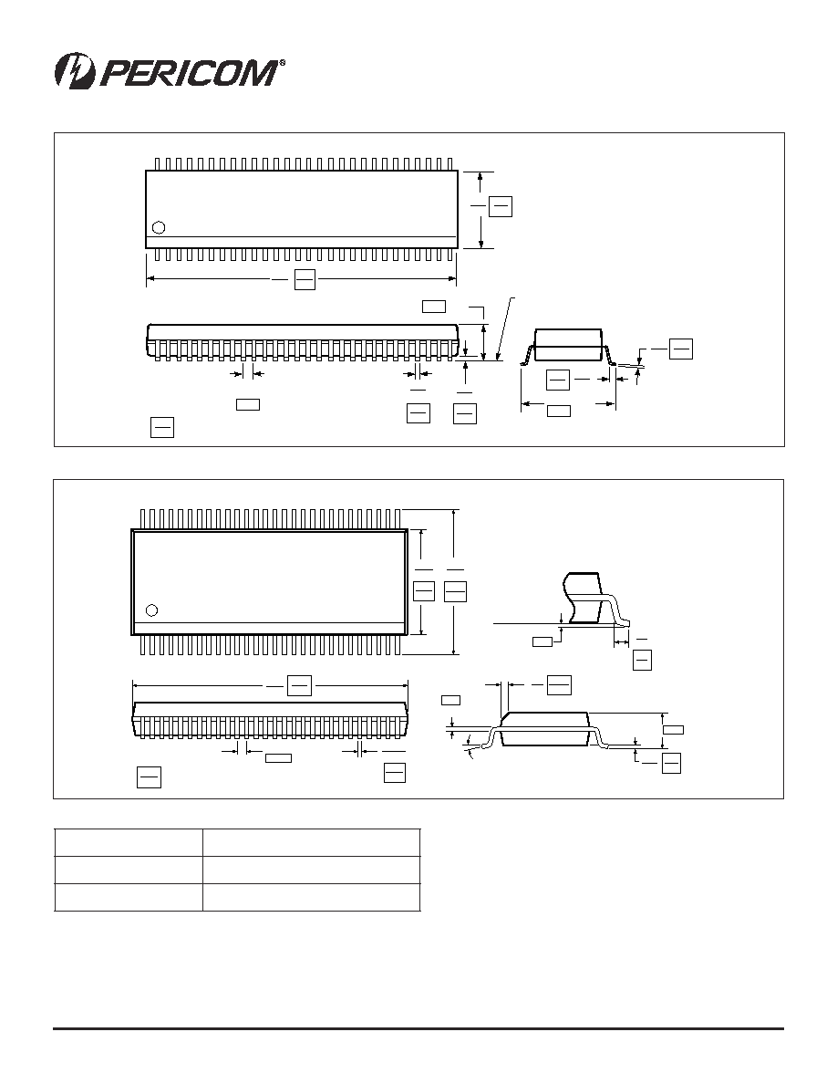
Packaging Mechanical: 56-Pin TSSOP (A) Package
Packaging Mechanical: 56-Pin SSOP (V) Package
.002
.006
SEATING PLANE
.007
.011
.004
.008
1
56
.236
.244
0.50
0.17
0.27
0.05
0.15
0.09
0.20
X.XX
X.XX
DENOTES DIMENSIONS
IN MILLIMETERS
.018
.030
0.45
0.75
.047
Max.
1.20
6.0
6.2
.547
.555
13.9
14.1
.319
8.1
.0197
BSC
BSC
0.25
0.20
.025 BSC
0.635
.008
.008
.016
0-8∞
0.20
0.40
.110 2.79
.010
Gauge Plane
.291
.299
X.XX
X.XX
DENOTES DIMENSIONS
IN MILLIMETERS
7.39
7.59
.396
.416
10.06
10.56
.02
.04
0.51
1.01
.015
.025
0.381
0.635
.720
.730
18.29
18.54
.008
.0135
0.20
0.34
1
56
x 45∞
Nom.
Max
Ordering Information
e
d
o
C
g
n
i
r
e
d
r
O
n
o
i
t
p
i
r
c
s
e
D
A
1
0
5
6
1
X
C
L
4
7
I
P
)
A
(
P
O
S
S
T
c
it
s
a
l
P
e
d
i
w
li
m
-
0
4
2
n
i
P
-
6
5
V
1
0
5
6
1
X
C
L
4
7
I
P
)
V
(
P
O
S
S
c
it
s
a
l
P
e
d
i
w
li
m
-
0
0
3
n
i
P
-
6
5