PI74LCX16646
1
PS2093B 09/20/02
12345678901234567890123456789012123456789012345678901234567890121234567890123456789012345678901212345678901234567890123456789012123456789012
12345678901234567890123456789012123456789012345678901234567890121234567890123456789012345678901212345678901234567890123456789012123456789012
PI74LCX16646
Fast CMOS 3.3V
16-Bit Registered Transceivers
Product Features
· Functionally compatible with FCT3, LVT, and 74
series 16646 families of products
· Tri-State outputs
· 5V Tolerant inputs and outputs
· 2.0V-3.6V V
CC
supply operation
· Balanced sink and source output drives (24 mA)
· Low ground bounce outputs
· Power Down High Impedance inputs and outputs
· Supports live insertion
· ESD Protection exceeds 2000V, Human Body Model
200V, Machine Model
· Packages available:
56-pin 240-mil wide plastic TSSOP (A)
56-pin 300-mil wide plastic SSOP (V)
Product Description
Pericom Semiconductor's PI74LCX series of logic circuits are
produced using the Company's advanced 0.6 micron CMOS
technology, achieving industry leading speed grades.
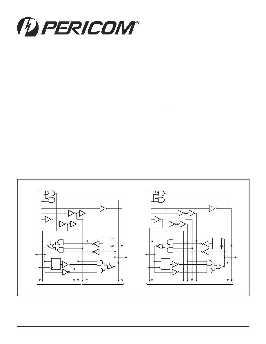
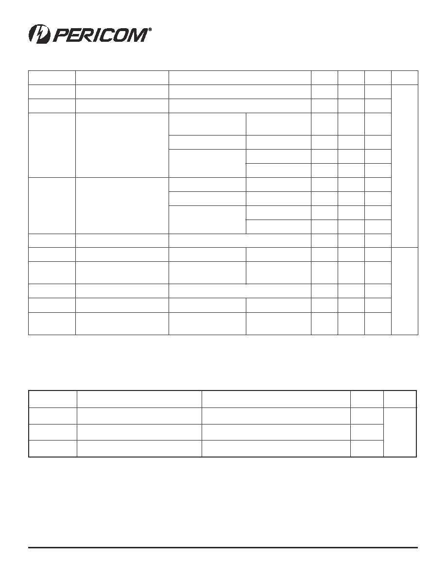
The PI74LCX16646 is a 16-bit non-inverting, bidirectional registered
bus transceiver organized as two independent 8-bit bus transceivers
designed with 3-state D-type flip-flops and control circuitry arranged
for multiplexed transmission of data directly from the data bus or
from the internal storage registers. Each 8-bit transceiver utilizes the
enable control (xOE) and direction pins (xDIR) to control the
transceiver functions. The Select (xSAB and xSBA) control pins are
used to select either real-time or stored data transfer. The circuitry
used for select control will eliminate the typical decoding glitch that
occurs in a multiplexer during the transition between real-time and
stored data. A low input level selects real-time data and a high
selects stored data.
The PI74LCX16646 can be driven from either 3.3V or 5.0V devices
allowing this device to be used as a translator in a mixed
3.3/5.0V system.
Logic Block Diagram
D
1
CLKAB
C
1
CLKBA
1
SBA
1
DIR
1
OE
1
SAB
D
C
A REG
B REG
1
B
0
1
A
0
TO 7 OTHER CHANNELS
D
2
CLKAB
C
2
CLKBA
2
SBA
2
DIR
2
OE
2
SAB
D
C
A REG
B REG
2
B
0
2
A
0
TO 7 OTHER CHANNELS
PI74LCX16646
Fast CMOS 3.3V 16-Bit Registered Transceivers
2
PS2093B 09/20/02
12345678901234567890123456789012123456789012345678901234567890121234567890123456789012345678901212345678901234567890123456789012123456789012
1
2
3
4
5
6
7
8
9
10
11
12
13
14
15
16
17
18
19
20
21
22
23
24
56
55
54
53
52
51
50
49
48
47
46
45
44
43
42
41
40
39
38
37
36
35
34
33
25
26
27
28
32
31
30
29
1
DIR
1
CLKAB
1
SAB
GND
1
A
1
1
A
2
V
CC
1
A
3
1
A
4
1
A
5
GND
1
A
6
1
A
7
1
A
8
2
A
1
1
A
2
1
A
3
GND
2
A
4
2
A
5
2
A
6
V
CC
2
A
7
2
A
8
GND
2
SAB
2
CLKAB
2
DIR
1
OE
1
CLKBA
1
SBA
GND
1
B
1
1
B
2
V
CC
1
B
3
1
B
4
1
B
5
GND
1
B
6
1
B
7
1
B
8
2
B
1
2
B
2
2
B
3
GND
2
B
8
2
B
7
2
B
6
V
CC
2
B
7
2
B
8
GND
2
SBA
2
CLKBA
2
OE
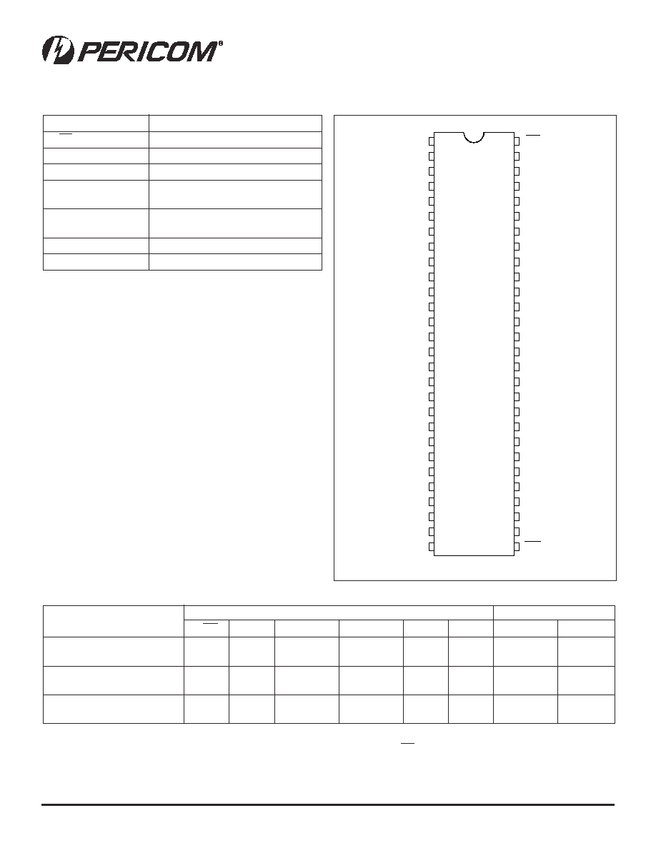
Product Pin Description
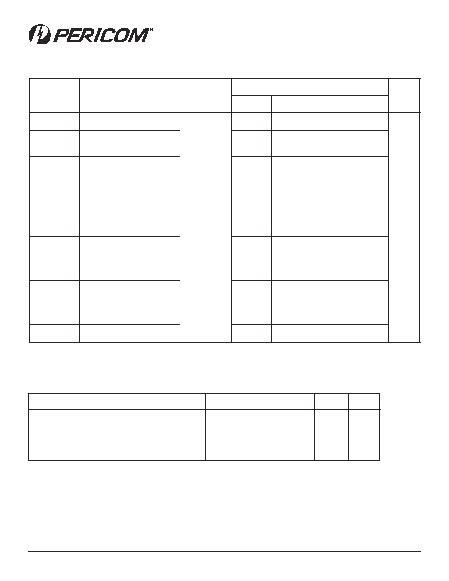
Product Pin Configuration
56-Pin
V56
A56
Pin Name
Description
xOE, xDIR
Output Enable Inputs (Active LOW)
xCLKAB, xCLKBA
Clock Pulse Inputs
xSAB, xSBA
Output Data Source Select Inputs
xAx
Data Register A Inputs
Data Register B Outputs
xBx
Data Register B Inputs
Data Register A Outputs
GND
Ground
V
CC
Power
Inputs
Data I/O
(1)
Function
xOE
xDIR
xCLKAB
xCLKBA
xSAB
xSBA
xAx
xBx
Isolation
H
X
H or L
H or L
X
X
Input
Input
Store A and B Data
H
X
X
X
Real Time B Data to A Bus
L
L
X
X
X
L
Output
Input
Stored B Data to A Bus
L
L
X
H or L
X
H
Real Time A Data to B Bus
L
H
X
X
L
X
Input
Output
Stored A Data to B Bus
L
H
H or L
X
H
X
Truth Table
(2)
Notes:
1. The data output functions may be enabled or disabled by various signals at the xOE or xDIR inputs. Data input functions are
always enabled, i.e., data at the bus pins will be stored on every LOW-to-HIGH transition on the clock inputs.
2. H = High Voltage Level, X = Don't Care,
L = Low Voltage Level,
= LOW-to-HIGH Transition
3
PS2093B 09/20/02
12345678901234567890123456789012123456789012345678901234567890121234567890123456789012345678901212345678901234567890123456789012123456789012
PI74LCX16646
Fast CMOS 3.3V 16-Bit Registered Transceivers
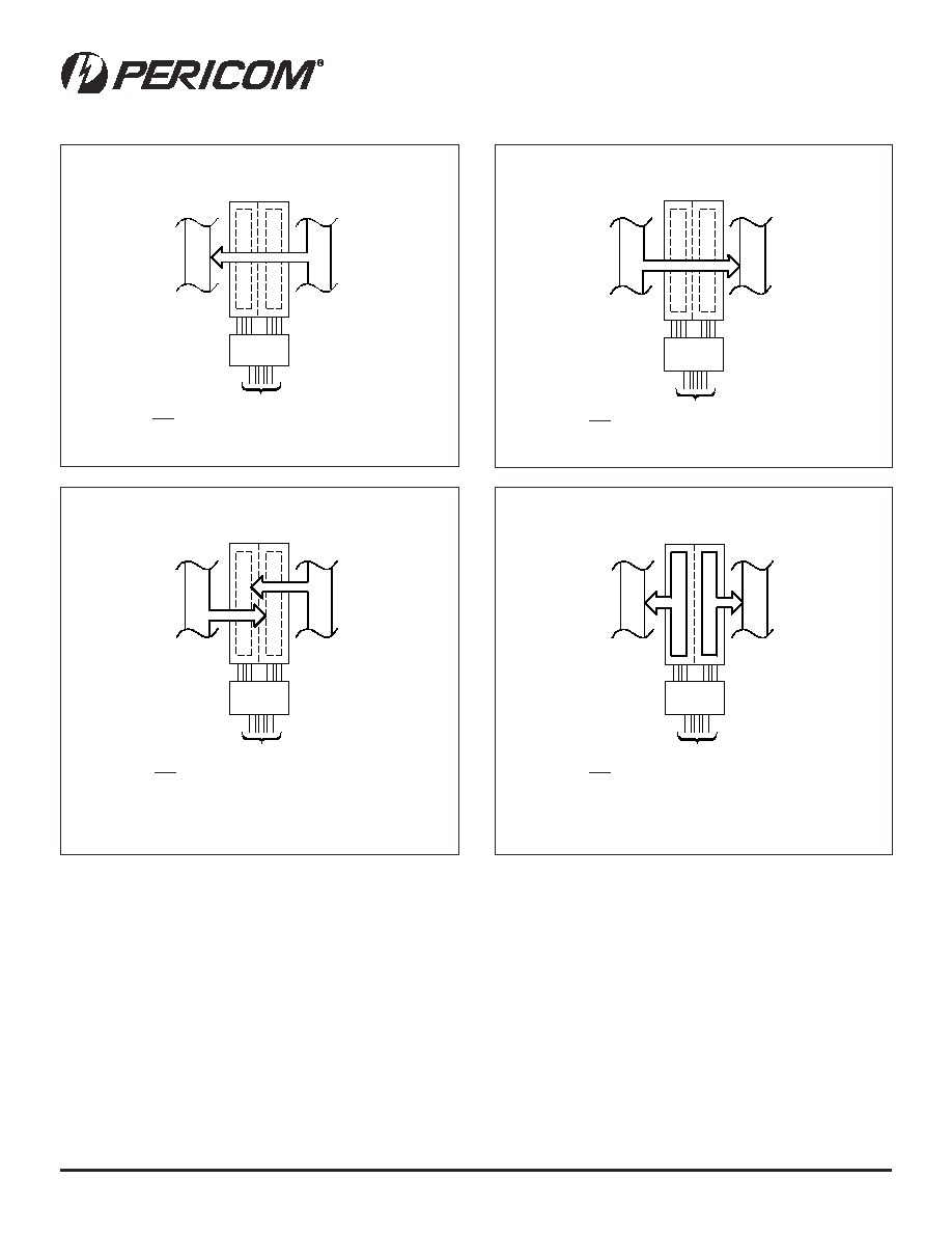
STORAGE FROM
A AND/OR B
TRANSFER STORES
DATA TO A AND/OR B
xDIR
xOE
CLKAB
CLKBA xSAB xSBA
H
L
X
X
X
L
L X
X
X
X
H
X
X
xDIR
(1)
xOE
CLKAB
CLKBA xSAB xSBA
L
L
X
H or L
X
H
H
L
H or L
X
H
X
REAL-TIME TRANSFER
BUS B TO A
REAL-TIME TRANSFER
BUS A TO B
xDIR
xOE
CLKAB
CLKBA xSAB xSBA
L
L
X
X
X
L
xDIR
xOE
CLKAB
CLKBA xSAB xSBA
H
L
X
X
L
X
BUS
A
BUS
B
BUS
A
BUS
B
BUS
A
BUS
B
BUS
A
BUS
B
Note:
1. Cannot transfer data to A bus and B bus simultaneously.
PI74LCX16646
Fast CMOS 3.3V 16-Bit Registered Transceivers
4
PS2093B 09/20/02
12345678901234567890123456789012123456789012345678901234567890121234567890123456789012345678901212345678901234567890123456789012123456789012
Maximum Ratings
(Above which the useful life may be impaired. For user guidelines, not tested.)
Note:
Stresses greater than those listed under
MAXIMUM RATINGS may cause permanent dam-
age to the device. This is a stress rating only and
functional operation of the device at these or any
other conditions above those indicated in the opera-
tional sections of this specification is not implied.
Exposure to absolute maximum rating conditions for
extended periods may affect reliability.
l
o
b
m
y
S
r
e
t
e
m
a
r
a
P
.
n
i
M
.
x
a
M
s
t
i
n
U
V
CC
e
g
a
tl
o
V
y
l
p
p
u
S
g
n
it
a
r
e
p
O
0
.
2
6
.
3
V
n
o
it
n
e
t
e
R
a
t
a
D
5
.
1
6
.
3
V
I
e
g
a
tl
o
V
t
u
p
n
I
0
5
.
5
V
O
e
g
a
tl
o
V
t
u
p
t
u
O
e
t
a
t
S
W
O
L
r
o
H
G
I
H
0
V
CC
e
t
a
t
S
-
I
R
T
0
5
.
5
I
OH
I
/
OL
t
n
e
r
r
u
C
t
u
p
t
u
O
V
CC
V
6
.
3
-
V
0
.
3
=
4
2
±
A
m
V
CC
V
7
.
2
=
2
1
±
T
A
e
r
u
t
a
r
e
p
m
e
T
g
n
it
a
r
e
p
O
r
i
A
-
e
e
r
F
-
0
4
5
8
+
°
C
/t
V
e
t
a
R
e
g
d
E
t
u
p
n
I
V
,
V
0
.
2
-
V
8
.
0
=
V
CC
V
0
.
3
=
0
0
1
V
/
s
n
Recommended Operating Conditions
Storage Temperature .............................................................. 65°C to +150°C
Ambient Temperature with Power Applied ............................. 40°C to +85°C
Supply Voltage to Ground Potential (Inputs & Vcc Only)....... 0.5V to +7.0V
Supply Voltage to Ground Potential (Outputs & D/O Only) ... 0.5V to +7.0V
DC Input Voltage ..................................................................... 0.5V to +7.0V
DC Output Current ............................................................................... 120 mA
Power Dissipation ..................................................................................... 1.0W
5
PS2093B 09/20/02
12345678901234567890123456789012123456789012345678901234567890121234567890123456789012345678901212345678901234567890123456789012123456789012
PI74LCX16646
Fast CMOS 3.3V 16-Bit Registered Transceivers
Notes:
1. For Max. or Min. conditions, use appropriate value specified under Electrical Characteristics for the applicable device type.
2. Typical values are at V
CC
= 3.3V, +25°C ambient.
3. Per TTL driven input; all other inputs at V
CC
or GND.
s
r
e
t
e
m
a
r
a
P
n
o
i
t
p
i
r
c
s
e
D
s
n
o
i
t
i
d
n
o
C
t
s
e
T
)
1
(
.
n
i
M
p
y
T
)
2
(
.
x
a
M
s
t
i
n
U
V
IH
e
g
a
tl
o
V
H
G
I
H
t
u
p
n
I
l
e
v
e
L
H
G
I
H
c
i
g
o
L
d
e
e
t
n
a
r
a
u
G
0
.
2
--
--
V
V
IL
e
g
a
tl
o
V
W
O
L
t
u
p
n
I
l
e
v
e
L
W
O
L
c
i
g
o
L
d
e
e
t
n
a
r
a
u
G
--
--
8
.
0
V
OH
e
g
a
tl
o
V
H
G
I
H
t
u
p
t
u
O
V
CC
6
.
3
-
7
.
2
=
I
OH
A
m
1
.
0
=
V
CC
-
0
-
2
.
--
--
V
CC
7
.
2
=
I
OH
A
m
2
1
=
2
.
2
--
--
V
CC
0
.
3
=
I
OH
A
m
8
1
=
4
.
2
--
--
I
OH
A
m
4
2
=
2
.
2
--
--
V
OL
e
g
a
tl
o
V
W
O
L
t
u
p
t
u
O
V
CC
6
.
3
-
7
.
2
=
I
OL
A
m
1
.
0
=
--
--
2
.
0
V
CC
7
.
2
=
I
OL
A
m
2
1
=
--
--
4
.
0
V
CC
0
.
3
=
I
OL
A
m
6
1
=
--
--
4
.
0
I
OL
A
m
4
2
=
--
--
5
5
.
0
V
IK
e
g
a
tl
o
V
e
d
o
i
D
p
m
a
l
C
V
CC
,.
n
i
M
=
I
IN
A
m
8
1
=
--
- 7
.
0
- 2
.
1
I
I
t
n
e
r
r
u
C
e
g
a
k
a
e
L
t
u
p
n
I
0 £ V
I
£
V
5
.
5
6
.
3
-
7
.
2
=
c
c
V
--
--
5
±
A
µ
I
OZ
e
g
a
k
a
e
L
t
u
p
t
u
O
e
t
a
t
S
-i
r
T
0 £ V
O
£
V
5
.
5
V
I
V
=
IH
V
r
o
IL
V
CC
6
.
3
-
7
.
2
=
--
--
5
±
I
OFF
e
l
b
a
s
i
D
n
w
o
D
r
e
w
o
P
V
CC
,
V
0
=
V
IN
V
r
o
OUT
V
5
.
5
--
--
0
1
I
CC
t
n
e
r
r
u
C
y
l
p
p
u
S
r
e
w
o
P
t
n
e
c
s
e
i
u
Q
V
CC
.
x
a
M
=
V
IN
V
r
o
D
N
G
=
CC
1
.
0
0
1
I
CC
t
n
e
r
r
u
C
y
l
p
p
u
S
r
e
w
o
P
t
n
e
c
s
e
i
u
Q
H
G
I
H
s
t
u
p
n
I
L
T
T
V
CC
.
x
a
M
=
V
IN
V
=
CC
V
6
.
0
)
3
(
¾
0
0
5
s
r
e
t
e
m
a
r
a
P
n
o
i
t
p
i
r
c
s
e
D
s
n
o
i
t
i
d
n
o
C
t
s
e
T
.
p
y
T
s
t
i
n
U
C
IN
e
c
n
a
ti
c
a
p
a
C
t
u
p
n
I
V
CC
V
,
n
e
p
O
=
I
V
r
o
V
0
=
CC
7
F
p
C
OUT
e
c
n
a
ti
c
a
p
a
C
t
u
p
t
u
O
V
CC
V
,
V
3
.
3
=
I
V
r
o
V
0
=
CC
8
C
PD
e
c
n
a
ti
c
a
p
a
C
n
o
it
a
p
i
s
s
i
D
r
e
w
o
P
V
CC
V
,
V
3
.
3
=
I
V
r
o
V
0
=
CC
,
z
H
M
0
1
=
F
0
2
Capacitance
DC Electrical Characteristics
(Over the Operating Range, T
A
=
-
40°C to +85°C, V
CC
= 2.7V to 3.6V)
PI74LCX16646
Fast CMOS 3.3V 16-Bit Registered Transceivers
6
PS2093B 09/20/02
12345678901234567890123456789012123456789012345678901234567890121234567890123456789012345678901212345678901234567890123456789012123456789012
Switching Characteristics over Operating Range
Note:
1. Skew between any two outputs, of the same package, switching in the same direction.
This parameter is guaranteed by design.
Dynamic Switching Characteristics (T
A
= +25°C)
Note:
1. Measured with n1 outputs switching from HIGH-to-LOW or LOW-to-HIGH. The remaining output is measured in
the LOW state.
s
r
e
t
e
m
a
r
a
P
n
o
i
t
p
i
r
c
s
e
D
s
n
o
i
t
i
d
n
o
C
t
s
e
T
)
1
(
.
p
y
T
s
t
i
n
U
V
OLP
e
g
a
tl
o
V
k
a
e
P
W
O
L
c
i
m
a
n
y
D
V
CC
C
,
V
3
.
3
=
L
F
p
0
5
=
V
IH
V
,
V
3
.
3
=
IL
V
0
=
8
.
0
V
V
OLV
e
g
a
tl
o
V
y
e
ll
a
V
W
O
L
c
i
m
a
n
y
D
V
CC
C
,
V
3
.
3
=
L
F
p
0
5
=
V
IH
V
,
V
3
.
3
=
IL
V
0
=
s
r
e
t
e
m
a
r
a
P
n
o
i
t
p
i
r
c
s
e
D
s
n
o
i
t
i
d
n
o
C
V
CC
V
3
.
0
±
V
3
.
3
=
V
CC
V
7
.
2
=
s
t
i
n
U
.
n
i
M
.
x
a
M
.
n
i
M
.
x
a
M
x
a
m
f
y
c
n
e
u
q
e
r
F
k
c
o
l
C
m
u
m
i
x
a
M
C
L
F
p
0
5
=
R
L
0
0
5
=
0
7
1
s
n
t
PHL
t
PLH
y
a
l
e
D
n
o
it
a
g
a
p
o
r
P
t
s
u
B
o
s
u
B
5
.
1
0
.
5
5
.
1
0
.
6
t
PHL
t
PLH
y
a
l
e
D
n
o
it
a
g
a
p
o
r
P
t
k
c
o
l
C
o
s
u
B
5
.
1
0
.
6
5
.
1
0
.
7
t
PHL
t
PLH
y
a
l
e
D
n
o
it
a
g
a
p
o
r
P
t
t
c
e
l
e
S
o
s
u
B
5
.
1
0
.
6
5
.
1
0
.
7
t
PZL
t
PZH
e
m
i
T
e
l
b
a
n
E
t
u
p
t
u
O
5
.
1
5
.
7
5
.
1
5
.
8
t
PLZ
t
PHZ
e
m
i
T
e
l
b
a
s
i
D
t
u
p
t
u
O
5
.
1
0
.
6
5
.
1
0
.
7
t
S
e
m
i
T
p
u
t
e
S
5
.
2
5
.
2
t
H
e
m
i
T
d
l
o
H
5
.
1
5
.
1
t
W
h
t
d
i
W
e
s
l
u
P
0
.
3
0
.
3
t
SK
(
O
)
w
e
k
S
t
u
p
t
u
O
o
t
t
u
p
t
u
O
)
1
(
0
.
1
7
PS2093B 09/20/02
12345678901234567890123456789012123456789012345678901234567890121234567890123456789012345678901212345678901234567890123456789012123456789012
PI74LCX16646
Fast CMOS 3.3V 16-Bit Registered Transceivers
Pericom Semiconductor Corporation
2380 Bering Drive · San Jose, CA 95131 · 1-800-435-2336 · Fax (408) 435-1100 · http://www.pericom.com
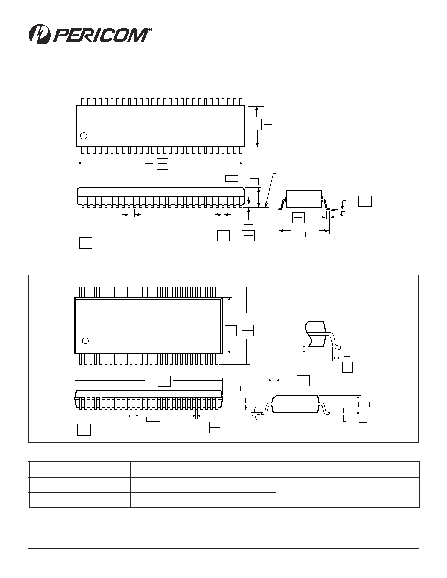
Packaging Mechanical: 56-Pin TSSOP (A) Package
Packaging Mechanical: 56-Pin SSOP (V) Package
.002
.006
SEATING PLANE
.007
.011
.004
.008
1
56
.236
.244
0.50
0.17
0.27
0.05
0.15
0.09
0.20
X.XX
X.XX
DENOTES DIMENSIONS
IN MILLIMETERS
.018
.030
0.45
0.75
.047
Max.
1.20
6.0
6.2
.547
.555
13.9
14.1
.319
8.1
.0197
BSC
BSC
0.25
0.20
.025 BSC
0.635
.008
.008
.016
0-8°
0.20
0.40
.110 2.79
.010
Gauge Plane
.291
.299
X.XX
X.XX
DENOTES DIMENSIONS
IN MILLIMETERS
7.39
7.59
.396
.416
10.06
10.56
.02
.04
0.51
1.01
.015
.025
0.381
0.635
.720
.730
18.29
18.54
.008
.0135
0.20
0.34
1
56
x 45°
Nom.
Max
r
e
b
m
u
N
t
r
a
P
n
o
i
t
p
i
r
c
s
e
D
e
g
n
a
R
g
n
i
t
a
r
e
p
O
A
6
4
6
6
1
X
C
L
4
7
I
P
P
O
S
S
T
c
it
s
a
l
p
e
d
i
w
li
m
-
0
4
2
,
n
i
p
-
6
5
C
°
5
8
o
t
C
°
0
4
V
6
4
6
6
1
X
C
L
4
7
I
P
P
O
S
S
c
it
s
a
l
p
e
d
i
w
li
m
-
0
0
3
,
n
i
p
-
6
5
Ordering Information